

Panasonic 2SC4606 Datasheet
Transistor
2SC4606
Silicon NPN epitaxial planer type
For low-frequency driver amplification
Complementary to 2SA1762
Features
■
●
High collector to emitter voltage V
●
Optimum for the driver stage of a low-frequenc y and 25 to 30W
output amplifier.
●
M type package allowing easy automatic and manual insertion as
well as stand-alone fixing to the printed circuit board.
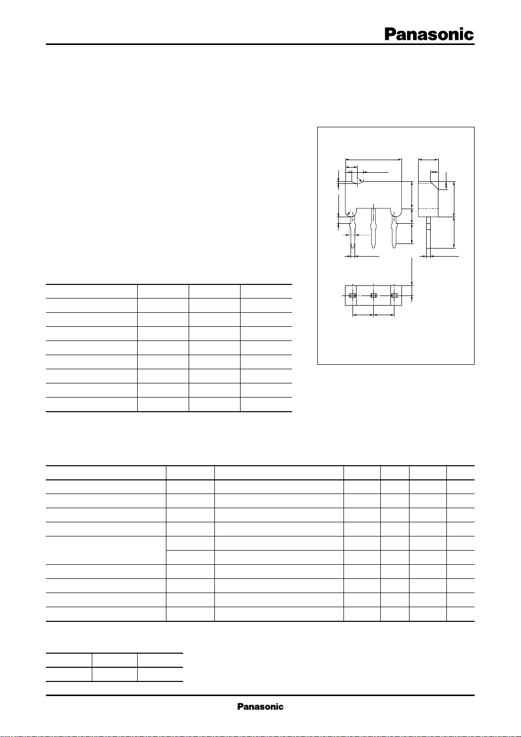
Absolute Maximum Ratings (Ta=25˚C)
■
Parameter
Collector to base voltage
Collector to emitter voltage
Emitter to base voltage
Peak collector current
Collector current
Collector power dissipation
Junction temperature
Storage temperature
*
Printed circuit board: Copper foil area of 1cm2 or more, and the board
thickness of 1.7mm for the collector portion
Symbol
V
CBO
V
CEO
V
EBO
I
CP
I
C
*
P
C
T
j
T
stg
.
CEO
Ratings
–55 ~ +150
80
80
5
1
0.5
1
150
Unit
V
V
V
A
A
W
˚C
˚C
6.9±0.1
1.5
1.5 R0.9
0.4
R0.9
R0.7
1.0±0.1
0.85
0.55±0.1 0.45±0.05
2.5 2.5
1:Base
2:Collector EIAJ:SC–71
3:Emitter M Type Mold Package
2.5±0.1
1.0
3.5±0.1
2.0±0.2
2.4±0.21.25±0.05
123
Unit: mm
1.0
4.1±0.2 4.5±0.1
Electrical Characteristics (Ta=25˚C)
■
Parameter
Collector cutoff current
Collector to base voltage
Collector to emitter voltage
Emitter to base voltage
Forward current transfer ratio
Collector to emitter saturation voltage
Base to emitter saturation voltage
Transition frequency
Collector output capacitance
*1
h
Rank classification
FE1
Symbol
I
CBO
V
CBO
V
CEO
V
EBO
h
FE1
h
FE2
V
CE(sat)
V
BE(sat)
f
T
C
ob
Rank R S
h
FE1
130 ~ 220 185 ~ 330
Conditions
VCB = 20V, IE = 0
IC = 10µA, IE = 0
IC = 100µA, IB = 0
IE = 10µA, IC = 0
*1
VCE = 10V, IC = 150mA
VCE = 5V, IC = 500mA
IC = 300mA, IB = 30mA
IC = 300mA, IB = 30mA
*2
*2
*2
*2
VCB = 10V, IE = –50mA, f = 200MHz
VCB = 10V, IE = 0, f = 1MHz
min
80
80
5
130
50
typ
max
330
100
0.2
0.85
120
11
*2
Pulse measurement
0.1
0.4
1.2
20
Unit
µA
V
V
V
V
V
MHz
pF
1
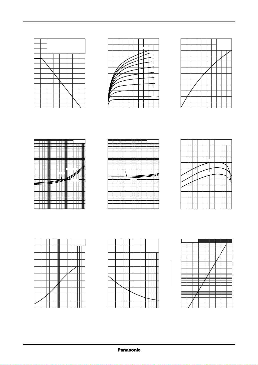
Transistor 2SC4606
PC — Ta IC — V
1.4
)
W
1.2
(
C
1.0
0.8
0.6
0.4
0.2
Collector power dissipation P
0
)
10
V
(
3
CE(sat)
1
0.3
0.1
0.03
0.01
0.003
0.001
Collector to emitter saturation voltage V
Printed circut board: Copper
foil area of 1cm
the board thickness of 1.7mm
for the collector portion.
0 16040 12080 14020 10060
2
or more, and
Ambient temperature Ta (˚C
V
— I
CE(sat)
1 10 100 10003 30 300
C
IC/IB=10
Ta=75˚C
25˚C
–25˚C
Collector current IC (mA
)
)
CE
1.2
1.0
)
A
(
0.8
C
0.6
0.4
Ta=25˚C
IB=10mA
9mA
Collector current I
0.2
0
0108264
Collector to emitter voltage VCE (V
V
— I
BE(sat)
100
)
V
(
30
BE(sat)
10
3
1
0.3
0.1
0.03
Base to emitter saturation voltage V
0.01
1 10 100 10003 30 300
25˚C
C
IC/IB=10
Ta=–25˚C
75˚C
Collector current IC (mA
8mA
7mA
6mA
5mA
4mA
3mA
2mA
1mA
)
1.2
1.0
)
A
(
0.8
C
0.6
0.4
Collector current I
0.2
0
0108264
)
Base current IB (mA
hFE — I
300
FE
250
200
150
100
50
Forward current transfer ratio h
0
1 10 100 10003 30 300
Collector current IC (mA
IC — I
Ta=75˚C
25˚C
–25˚C
B
VCE=10V
Ta=25˚C
)
C
VCE=10V
)
fT — I
200
)
160
MHz
(
T
120
80
40
Transition frequency f
0
–1 –3 –10 –30 –100
Emitter current IE (mA
2
E
VCB=10V
Ta=25˚C
50
)
pF
(
40
ob
Cob — V
CB
IE=0
f=1MHz
Ta=25˚C
4
10
3
10
VCB=20V
I
CBO
— Ta
)
30
20
10
)
Ta
(
Ta=25˚C
(
CBO
I
CBO
I
2
10
10
Collector output capacitance C
0
1 3 10 30 100
)
Collector to base voltage VCB (V
)
1
0 18060 120
Ambient temperature Ta (˚C
)
 Loading...