

Panasonic 2SC3980A, 2SC3980 Datasheet
Po wer Transistors
2SC3980, 2SC3980A
Silicon NPN triple diffusion planar type
For high breakdown voltage high-speed switching
Features
■
●
High-speed switching
●
High collector to base voltage V
●
Wide area of safe operation (ASO)
●
Satisfactory linearity of foward current transfer ratio h
●
Full-pack package which can be installed to the heat sink with
one screw
Absolute Maximum Ratings (T
■
Parameter
Collector to
base voltage
Collector to
emitter voltage
Collector to emitter voltage
Emitter to base voltage
Peak collector current
Collector current
Base current
Collector power
dissipation
Junction temperature
Storage temperature
2SC3980
2SC3980A
2SC3980
2SC3980A
TC=25°C
Ta=25°C
Symbol
V
CBO
V
CES
V
CEO
V
EBO
I
CP
I
C
I
B
P
C
T
j
T
stg
CBO
=25˚C)
C
Ratings
900
1000
900
1000
800
7
6
4
2
70
3
150
–55 to +150
FE
Unit
V
V
V
V
A
A
A
W
˚C
˚C
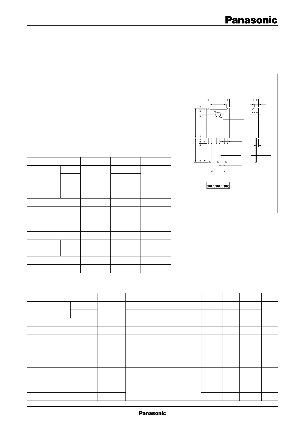
21.0±0.516.2±0.5
3.5 0.715.0±0.2
12.5
Solder Dip
15.0±0.3
11.0±0.2
φ3.2±0.1
2.0±0.2
1.1±0.1
5.45±0.3
10.9±0.5
321
TOP–3 Full Pack Package(a)
Unit: mm
5.0±0.2
3.2
2.0±0.1
0.6±0.2
1:Base
2:Collector
3:Emitter
Electrical Characteristics (T
■
Parameter
Collector cutoff
current
2SC3980
2SC3980A
Emitter cutoff current
Collector to emitter voltage
Forward current transfer ratio
Collector to emitter saturation voltage
Base to emitter saturation voltage
Transition frequency
Turn-on time
Storage time
Fall time
Symbol
I
CBO
I
EBO
V
CEO
h
FE1
h
FE2
V
CE(sat)
V
BE(sat)
f
T
t
on
t
stg
t
f
=25˚C)
C
Conditions
VCB = 900V, IE = 0
VCB = 1000V, IE = 0
VEB = 7V, IC = 0
IC = 10mA, IB = 0
VCE = 5V, IC = 0.1A
VCE = 5V, IC = 2A
IC = 2A, IB = 0.4A
IC = 2A, IB = 0.4A
VCE = 5V, IC = 0.2A, f = 1MHz
IC = 2A, IB1 = 0.4A, IB2 = – 0.8A,
VCC = 250V
min
800
8
6
typ15max
50
50
50
1.5
1.5
0.7
2.5
0.3
Unit
µA
µA
V
V
V
MHz
µs
µs
µs
1
Po wer Transistors 2SC3980, 2SC3980A
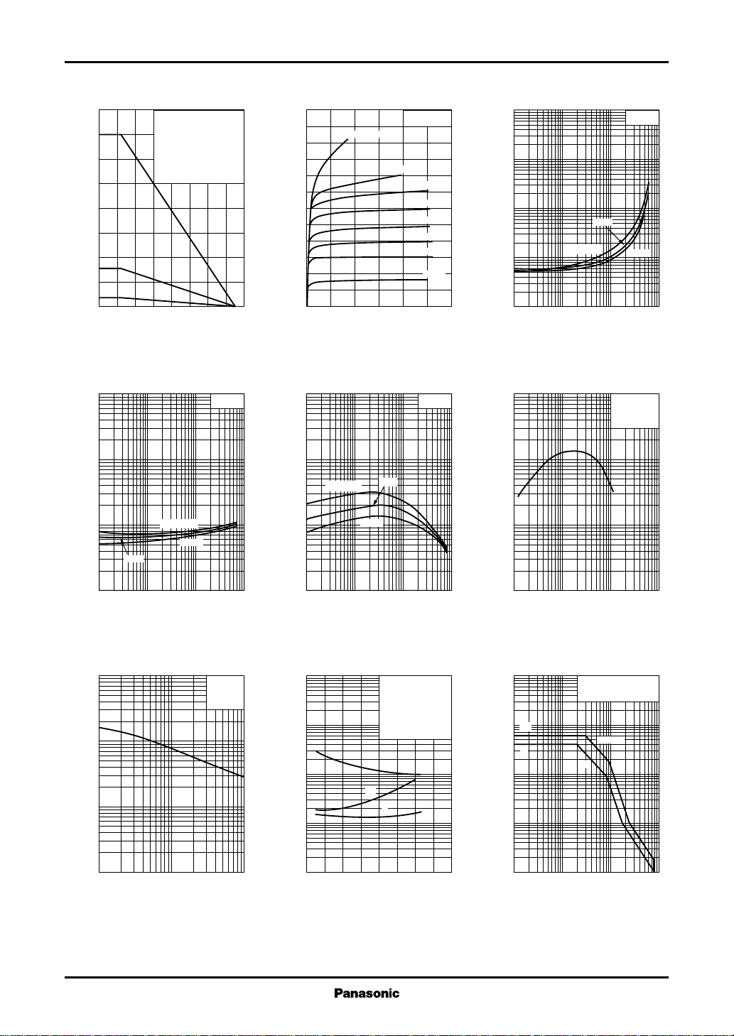
PC—Ta IC—V
80
)
(1)
70
W
(
C
60
50
40
30
20
(2)
10
Collector power dissipation P
(3)
0
0 16040 12080 14020 10060
Ambient temperature Ta (˚C
100
)
V
(
30
BE(sat)
10
3
(1) TC=Ta
(2) With a 100 × 100 × 2mm
Al heat sink
(3) Without heat sink
=3W)
(P
C
V
BE(sat)—IC
IC/IB=5
CE
6
5
)
A
(
4
C
3
2
IB=1000mA
Collector current I
1
0
012108264
)
Collector to emitter voltage VCE (V
hFE—I
1000
FE
300
100
TC=100˚C
30
TC=25˚C
500mA
400mA
300mA
200mA
150mA
100mA
50mA
C
VCE=5V
25˚C
)
100
V
(
30
CE(sat)
10
0.3
0.1
0.03
0.01
Collector to emitter saturation voltage V
)
100
)
30
MHz
(
T
10
V
CE(sat)—IC
3
1
0.01 0.1 1 100.03 0.3 3
25˚C
TC=100˚C
Collector current IC (A
fT—I
C
VCE=5V
f=1MHz
T
C
3
IC/IB=5
–25˚C
)
=25˚C
25˚C
Cob—V
TC=100˚C
–25˚C
CB
)
IE=0
f=1MHz
=25˚C
T
C
1
0.3
Base to emitter saturation voltage V
0.1
0.01 0.1 1 100.03 0.3 3
Collector current IC (A
1000
)
pF
(
300
ob
100
30
10
3
Collector output capacitance C
1
1 3 10 30 100
Collector to base voltage VCB (V
10
3
Forward current transfer ratio h
1
0.01 0.1 1 100.03 0.3 3
Collector current IC (A
ton, t
100
30
)
µs
(
10
f
,t
stg
3
,t
on
1
0.3
0.1
Switching time t
0.03
0.01
082647153
)
Collector current IC (A
–25˚C
, tf — I
stg
t
on
C
Pulsed tw=1ms
Duty cycle=1%
=5
I
C/IB
=–IB2)
(2I
B1
V
=200V
CC
=25˚C
T
C
t
stg
t
f
1
0.3
Transition frequency f
0.1
0.01 0.1 1 100.03 0.3 3
)
Collector current IC (A
)
Area of safe operation (ASO)
100
30
)
10
I
A
CP
(
C
I
3
C
1
0.3
0.1
Collector current I
0.03
0.01
1 10 100 10003 30 300
)
Collector to emitter voltage VCE (V
Non repetitive pulse
=25˚C
T
C
t=10ms
DC
)
2
 Loading...