


Panasonic 2SC3938G User Manual
This product complies with the RoHS Directive (EU 2002/95/EC).
Transistors
2SC3938G
Silicon NPN epitaxial planar type
For high-speed switching
■ Features
• Low collector-emitter saturation voltage V
• S-Mini type package, allowing downsizing of the equipment and
automatic insertion through the tape packing
CE(sat)
■ Package
• Code
SMini3-F2
• Marking Symbol: 2Y
• Pin Name
■ Absolute Maximum Ratings Ta = 25°C
Parameter Symbol Rating Unit
Collector-base voltage (Emitter open) V
Collector-emitter voltage (E-B short) V
Emitter-base voltage (Collector open) V
Collector current I
Peak collector current I
Collector power dissipation P
Junction temperature T
Storage temperature T
CBO
CES
EBO
C
CP
C
j
−55 to +150 °C
stg
40 V
40 V
5V
100 mA
300 mA
150 mW
150 °C
1. Base
2. Emitter
3. Collector
■ Electrical Characteristics Ta = 25°C ± 3°C
Parameter Symbol Conditions Min Typ Max Unit
Collector-base cutoff current (Emitter open)
Emitter-base cutoff current (Collector open)
Forward current transfer ratio
*
Collector-emitter saturation voltage V
Base-emitter saturation voltage V
Transition frequency f
Collector output capacitance C
(Common base, input open circuited)
Turn-on time t
Turn-off time t
Storage time t
Note) 1. Measuring methods are based on JAPANESE INDUSTRIAL STANDARD JIS C 7030 measuring methods for transistors.
2.*: Rank classification
Rank Q R
h
FE
60 to 120 90 to 200
I
CBO
I
EBO
h
FE
CE(sat)IC
BE(sat)IC
T
ob
on
off
stg
VCB = 40 V, IE = 0 0.1 µA
VEB = 4 V, IC = 0 0.1 µA
VCE = 1 V, IC = 10 mA 60 200
= 10 mA, IB = 1 mA 0.17 0.25 V
= 10 mA, IB = 1 mA 1 V
VCB = 10 V, IE = −10 mA, f = 200 MHz 450 MHz
VCB = 10 V, IE = 0, f = 1 MHz 2 6 pF
Refer to the measurement circuit 17 ns
17 ns
10 ns
Publication date: April 2007 SJC00364AED
1
2SC3938G
This product complies with the RoHS Directive (EU 2002/95/EC).
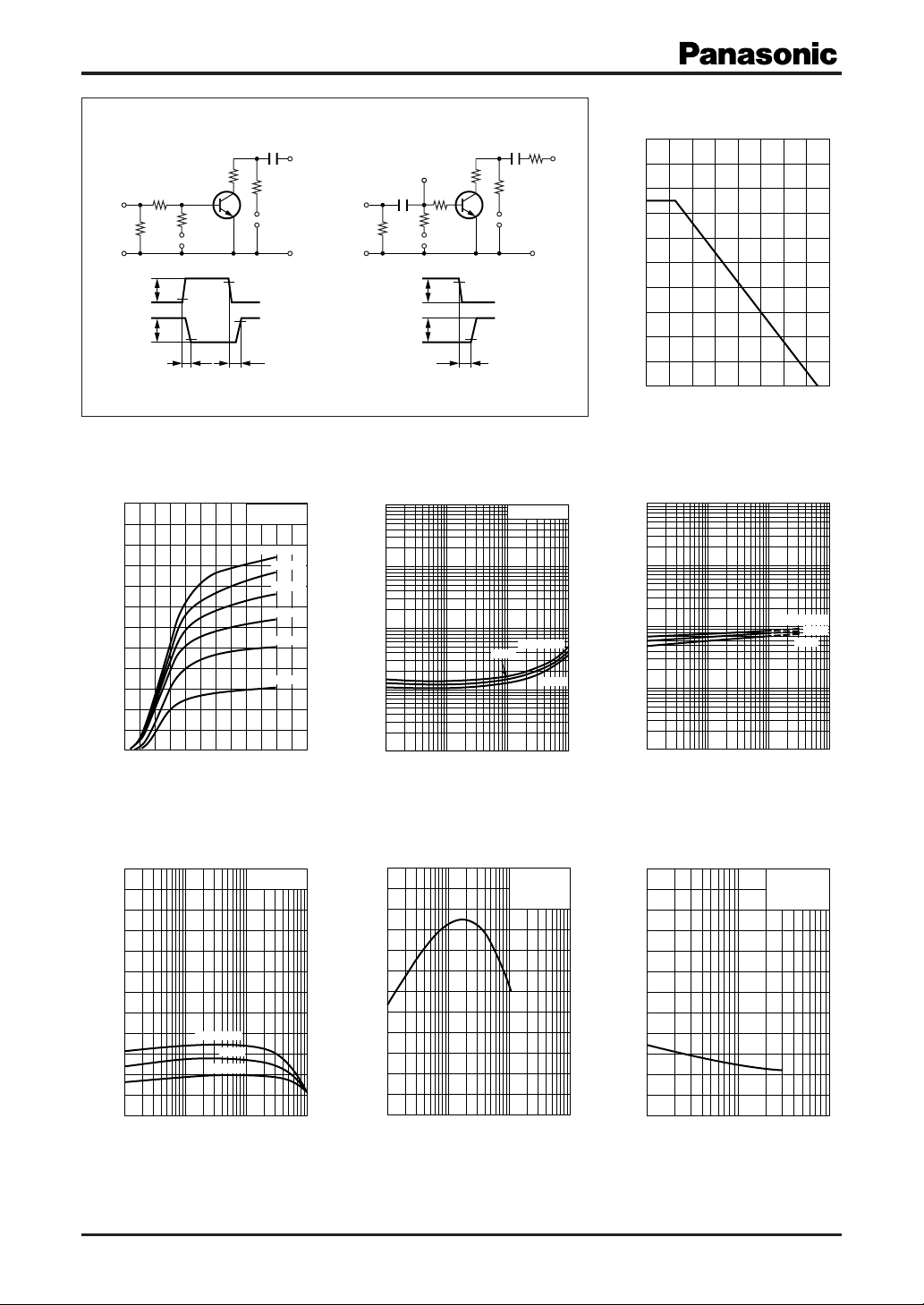
Measurement circuit
ton , t
test circuit t
off
220 Ω
3.3 kΩ
V
= 10 V
IN
50 Ω
V
V
OUT
120
100
)
mA
(
80
C
60
40
Collector current I
20
0
0 1.21.00.80.2 0.60.4
Collector-emitter voltage VCE (V
3.3 kΩ
VBB = −3 V
10%
90%
t
on
IC V
10%
CE
IN
0.1 µF
50 Ω
V
= 3 V
CC
90%
t
off
Ta = 25°C
IB = 3.0 mA
2.5 mA
2.0 mA
1.5 mA
1.0 mA
0.5 mA
PC T
BE(sat)
I
a
C
Ta = −25°C
75°C
)
)
25°C
test circuit
stg
V
OUT
V
= 10 V
IN
50 Ω
0.1 µF
V
V
OUT
A
910 Ω
500 Ω
500 Ω
= 2 V
V
BB
IN
t
stg
10%
10%
0.1 µF
90 Ω
V
CC
1 kΩ
= 10 V
V
OUT
(Waveform at A)
200
)
mW
160
(
C
120
80
40
Collector power dissipation P
0
0 16040 12080 14020 10060
Ambient temperature Ta (°C
V
I
100
CE(sat)
)
V
(
CE(sat)
10
1
0.1
Collector-emitter saturation voltage V
0.01
)
0.1 1 10 100
Collector current IC (mA
25°C
C
IC / IB = 10
Ta = 75°C
−25°C
)
100
)
V
(
BE(sat)
10
1
0.1
Base-emitter saturation voltage V
0.01
V
1 10 100 1 000
Collector current IC (mA
h
I
600
500
FE
400
300
200
Forward current transfer ratio h
100
0
0.1 1 10 100
FE
Ta = 75°C
25°C
−25°C
Collector current IC (mA
2
C
VCE = 1 V
)
600
fT I
500
)
MHz
(
400
T
300
200
Transition frequency f
100
0
−1 −10 −100
Emitter current IE (mA
SJC00364AED
E
VCB = 10 V
= 25°C
T
a
)
(pF)
ob
C
Collector output capacitance
−1 000
(Common base, input open circuited)
Cob V
6
5
4
3
2
1
0
110100
Collector-base voltage VCB (V
CB
IE = 0
f = 1 MHz
= 25°C
T
a
)