

Panasonic 2SC3932 Datasheet
Transistors
2SC3932
Silicon NPN epitaxial planer type
For high-frequency amplification / oscillation / mixing
■ Features
• High transition frequency f
• S-mini type package, allowing downsizing of the equipment and
automatic insertion through the tape packing and the magazine
packing.
■ Absolute Maximum Ratings Ta = 25°C
Parameter Symbol Rating Unit
Collector to base voltage V
Collector to emitter voltage V
Emitter to base voltage V
Collector current I
Collector power dissipation P
Junction temperature T
Storage temperature T
T
CBO
CEO
EBO
C
C
j
stg
30 V
20 V
3V
50 mA
150 mW
150 °C
−55 to +150 °C
+0.1
0.3
–0.0
132
(0.65)
(0.65)
1.3
±0.1
2.0
±0.2
10°
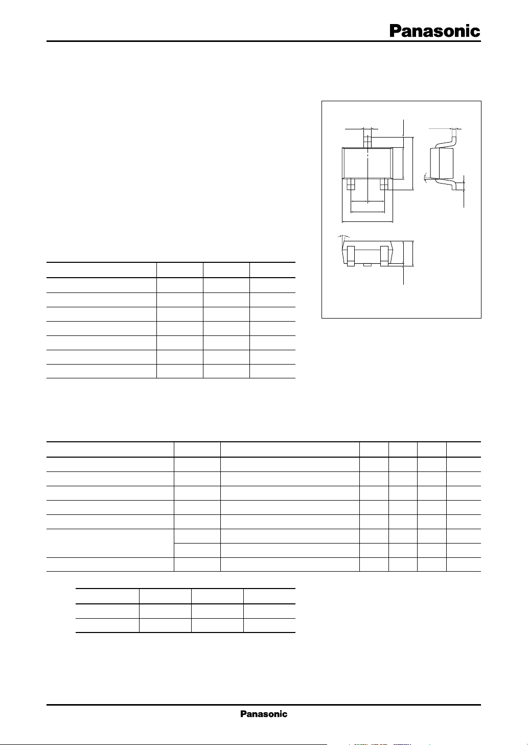
1: Base
2: Emitter EIAJ: SC-70
3: Collector S-Mini Type Package
Marking Symbol: R
(0.425)
±0.10
1.25
+0.2
±0.1
0.9
0.9
0 to 0.1
Unit: mm
+0.10
0.15
–0.05
±0.1
2.1
5°
±0.1
0.2
–0.1
■ Electrical Characteristics Ta = 25°C ± 3°C
Parameter Symbol Conditions Min Typ Max Unit
Collector to base voltage V
Emitter to base voltage V
CBO
EBO
Forward current transfer ratio h
Base to emitter voltage V
Transition frequency
Common emitter reverse transfer
capacitance
*
f
C
C
Power gain PG VCB = 10 V, IE = −1 mA, f = 200 MHz 20 dB
Note)*: Rank classification
Rank T S No-rank
fT (MHz) 800 to 1 400 1 000 to 1 600 800 to 1 600
Marking symbol RT RS R
Product of no-rank is not classified and have no indication for rank.
IC = 100 µA, IE = 030 V
IE = 10 µA, IC = 03V
VCB = 10 V, IE = −2 mA 25 250
FE
VCB = 10 V, IE = −2 mA 720 mV
BE
VCB = 10 V, IE = −15 mA, f = 200 MHz 800 1 600 MHz
T
VCB = 10 V, IE = −1 mA, f = 10.7 MHz 1 1.5 pF
re
VCE= 6 V, IC = 0, f = 1 MHz 0.8 pF
rb
1
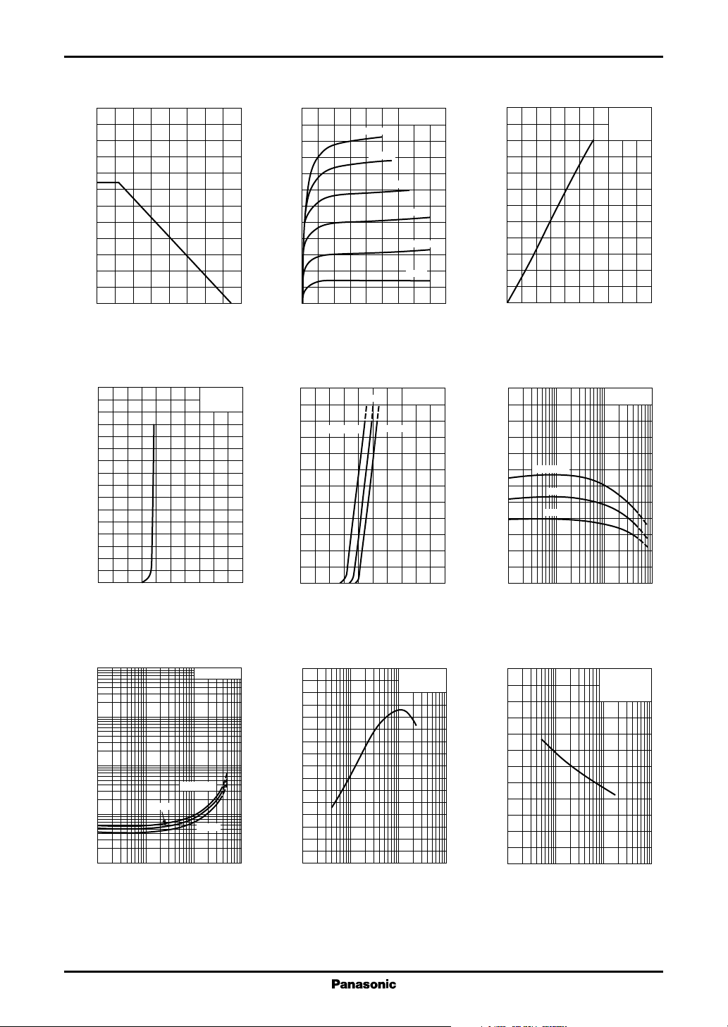
2SC3932 Transistors
PC T
240
200
(mW)
C
160
120
80
40
Collector power dissipation P
0
0 16040 12080
Ambient temperature Ta (°C)
IB V
400
350
300
250
(µA)
B
200
150
Base current I
100
50
a
BE
VCE = 10 V
= 25°C
T
a
IC V
24
20
16
(mA)
C
12
8
CE
IB = 300 µA
250 µA
200 µA
Collector current I
4
0
0 4 8 12 162 6 10 14 18
Collector to emitter voltage VCE (V)
IC V
60
50
40
(mA)
C
30
20
Ta = 75°C
BE
25°C
−25°C
Collector current I
10
Ta = 25°C
150 µA
100 µA
50 µA
V
= 10 V
CE
IC I
B
(mA)
C
24
20
16
12
8
Collector current I
4
0
0 500400300200100
Base current IB (µA)
hFE I
240
200
FE
160
Ta = 75°C
120
80
Forward current transfer ratio h
40
25°C
−25°C
VCE = 10 V
T
C
VCE = 10 V
= 25°C
a
0
0 2.01.61.20.80.4
Base to emitter voltage VBE (V)
V
100
(V)
30
CE(sat)
10
3
1
0.3
0.1
0.03
0.01
Collector to emitter saturation voltage V
0.1 0.3
Collector current IC (mA)
2
I
CE(sat)
1 3 10 30 100
C
IC / IB = 10
Ta = 75°C
25°C
–25°C
0
0 2.01.61.20.80.4
Base to emitter voltage VBE (V)
fT I
1 600
1 400
1 200
(MHz)
T
1 000
800
600
400
E
VCB = 10 V
T
= 25°C
a
Transition frequency f
200
0
− 0.1 − 0.3 −1 −3 −10 −30 −100
Emitter current IE (mA)
0
0.1 0.3
1 3 10 30 100
Collector current IC (mA)
Cre V
2.4
(pF)
re
2.0
1.6
1.2
0.8
0.4
0
Common emitter reverse transfer capacitance C
0.1 0.3 1 3 10 30 100
CE
IC = 1 mA
f = 10.7 MHz
= 25°C
T
a
Collector to emitter voltage VCE (V)
 Loading...