

Panasonic 2SC3930 Datasheet
Transistor
2SC3930
Silicon NPN epitaxial planer type
For high-frequency amplification
Complementary to 2SA1532
Features
■
●
Optimum for RF amplification of FM/AM radios.
●
High transition frequency fT.
●
S-Mini type package, allowing downsizing of the equipment and
automatic insertion through the tape packing and the magazine
packing.
Absolute Maximum Ratings (Ta=25˚C)
■
Parameter
Collector to base voltage
Collector to emitter voltage
Emitter to base voltage
Collector current
Collector power dissipation
Junction temperature
Storage temperature
Symbol
V
CBO
V
CEO
V
EBO
I
C
P
C
T
j
T
stg
Ratings
30
20
5
30
150
150
–55 ~ +150
Unit
V
V
V
mA
mW
˚C
˚C
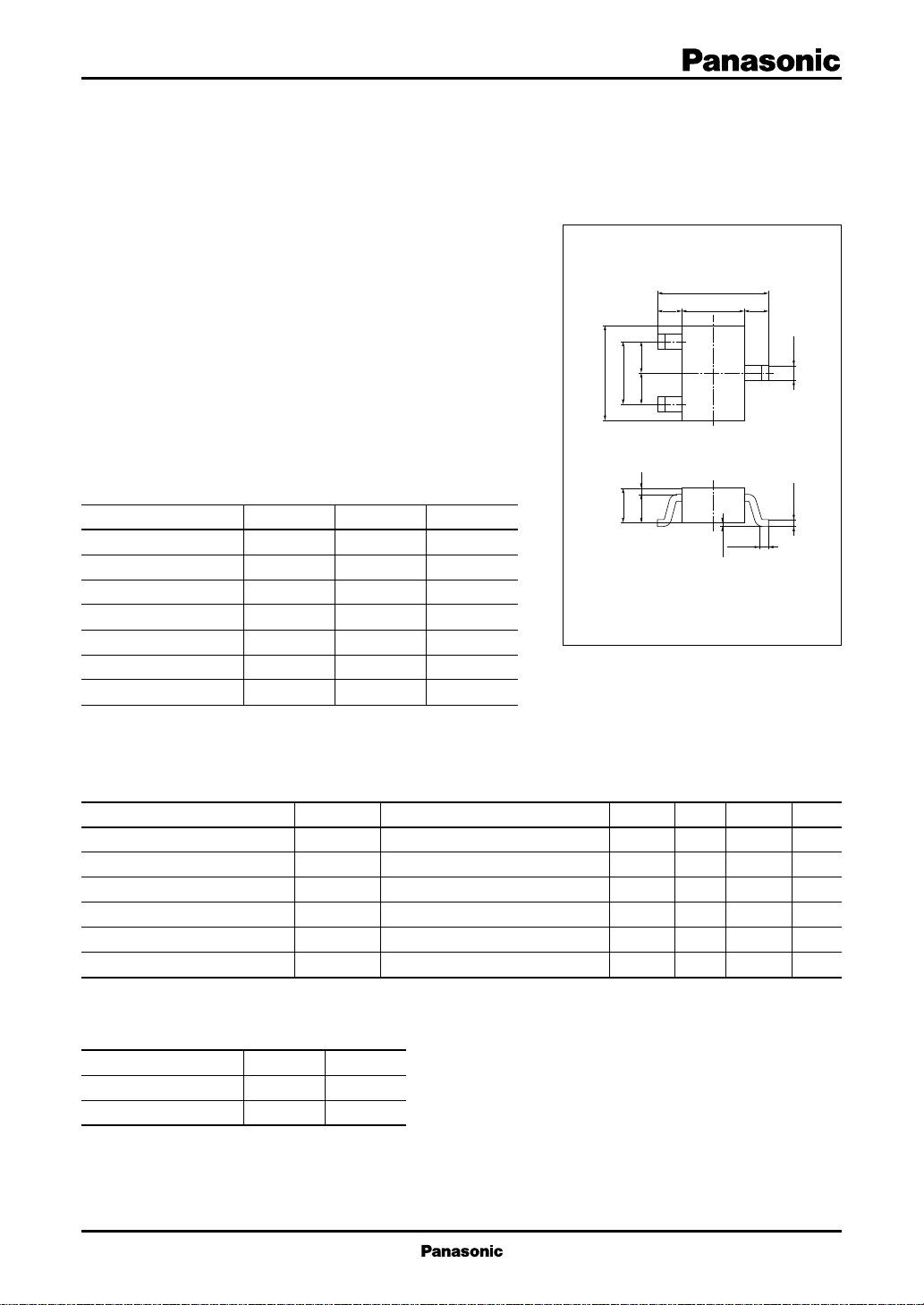
2.1±0.1
1.25±0.1 0.4250.425
1
1.3±0.10.9±0.1
2.0±0.2
0.650.2 0.65
2
0.7±0.1
0.2±0.1
0 to 0.1
1:Base
2:Emitter EIAJ:SC–70
3:Collector S–Mini Type Package
Marking symbol : V
3
Unit: mm
–0
+0.1
0.3
–0.05
+0.1
0.15
Electrical Characteristics (Ta=25˚C)
■
Parameter
Collector cutoff current
Forward current transfer ratio
Transition frequency
Noise figure
Reverse transfer impedance
Common emitter reverse transfer capacitance
*
hFE Rank classification
Symbol
I
CBO
h
FE
f
T
NF
Z
rb
C
re
Rank B C
h
FE
70 ~ 140 110 ~ 220
Marking Symbol VB VC
Conditions
VCB = 10V, IE = 0
*
VCB = 10V, IE = –1mA
VCB = 10V, IE = –1mA, f = 200MHz
VCB = 10V, IE = –1mA, f = 5MHz
VCB = 10V, IE = –1mA, f = 2MHz
VCE = 10V, IC = 1mA, f = 10.7MHz
min
70
150
typ
250
2.8
22
0.9
max
0.1
220
4
50
1.5
Unit
µA
MHz
dB
Ω
pF
1
Transistor
2SC3930
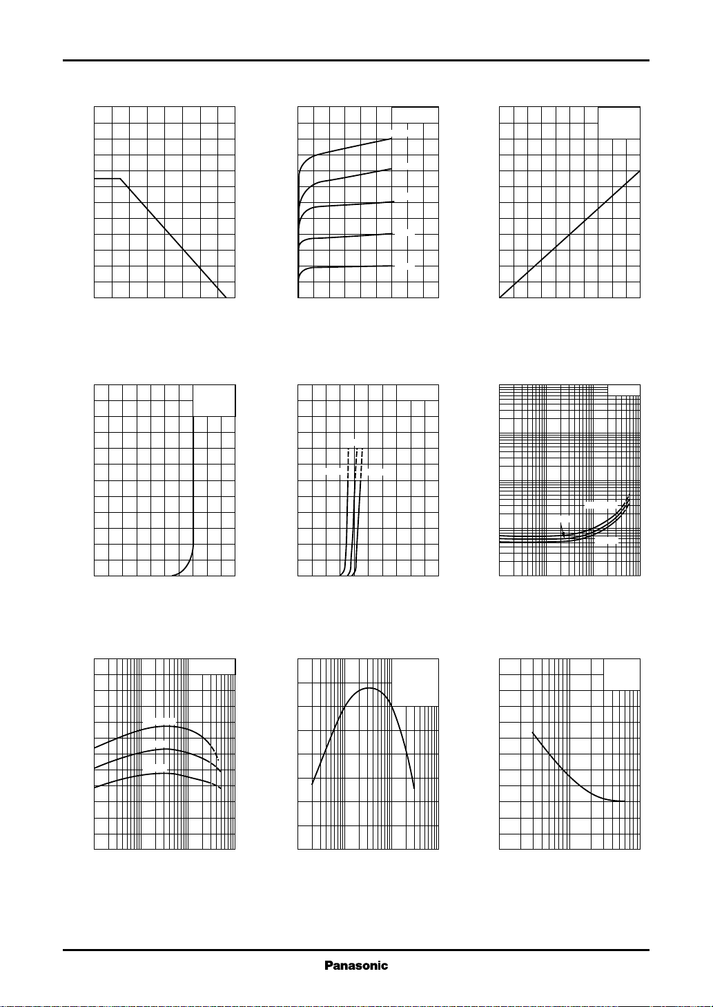
PC — Ta IC — V
240
)
mW
200
(
C
160
120
80
40
Collector power dissipation P
0
0 16040 12080 14020 10060
Ambient temperature Ta (˚C
IB — V
BE
120
100
)
µA
(
80
B
60
VCE=10V
Ta=25˚C
CE
12
10
)
mA
(
8
C
6
4
Collector current I
2
0
018612
)
Collector to emitter voltage VCE (V
IC — V
60
50
)
mA
(
40
C
30
25˚C
Ta=75˚C
Ta=25˚C
IB=100µA
80µA
60µA
40µA
20µA
BE
VCE=10V
–25˚C
15.0
12.5
)
mA
(
10.0
C
Collector current I
)
)
100
V
(
CE(sat)
7.5
5.0
2.5
0
0 1008020 6040
30
10
3
1
IC — I
B
VCE=10V
Ta=25˚C
Base current IB (µA
V
— I
CE(sat)
C
)
IC/IB=10
40
Base current I
20
0
01.00.80.2 0.60.4
Base to emitter voltage VBE (V
hFE — I
C
240
FE
200
160
120
80
40
Forward current transfer ratio h
0
0.1 1 10 1000.3 3 30
Ta=75˚C
25˚C
–25˚C
VCE=10V
Collector current IC (mA
20
Collector current I
10
0
0 2.01.60.4 1.20.8
)
)
Base to emitter voltage VBE (V
fT — I
E
400
350
)
MHz
300
(
T
250
200
150
100
Transition frequency f
50
0
– 0.1 –1 –10 –100– 0.3 –3 –30
Emitter current IE (mA
VCB=10V
f=100MHz
Ta=25˚C
)
)
0.3
0.1
0.03
0.01
Collector to emitter saturation voltage V
0.1 1 10 1000.3 3 30
Collector current IC (mA
Zrb — I
60
)
Ω
(
50
rb
40
30
20
10
Reverse transfer impedance Z
0
– 0.1 – 0.3 –1 –3 –10
Emitter current IE (mA
25˚C
Ta=75˚C
E
–25˚C
)
VCB=10V
f=2MHz
Ta=25˚C
)
2
 Loading...