

Panasonic 2SC3829 Datasheet
Transistor
2.8
+0.2
–0.3
1.5
+0.25
–0.050.65±0.15 0.65±0.15
3
1
2
0.950.95
1.9±0.2
0.4
+0.1
–0.05
1.1
+0.2
–0.1
0.8
0.4±0.2
0 to 0.1
0.16
+0.1
–0.06
1.45
0.1 to 0.3
2.9
+0.2
–0.05
2SC3829
Silicon NPN epitaxial planer type
For UHF band low-noise amplification
Features
■
●
Low noise figure NF.
●
High gain.
●
High transition frequency fT.
●
Mini type package, allowing downsizing of the equipment and
automatic insertion through the tape packing and the magazine
packing.
Absolute Maximum Ratings (Ta=25˚C)
■
Parameter
Collector to base voltage
Collector to emitter voltage
Emitter to base voltage
Collector current
Collector power dissipation
Junction temperature
Storage temperature
Symbol
V
CBO
V
CEO
V
EBO
I
C
P
C
T
j
T
stg
Ratings
15
10
2
80
200
150
–55 ~ +150
Unit
V
V
V
mA
mW
˚C
˚C
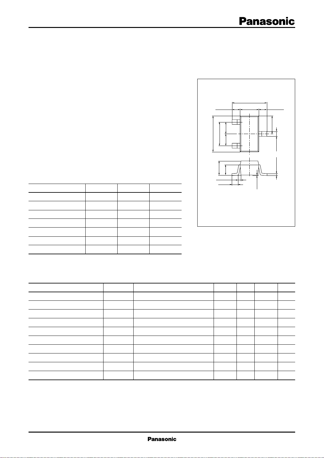
Unit: mm
1:Base JEDEC:TO–236
2:Emitter EIAJ:SC–59
3:Collector Mini T ype Package
Marking symbol : 3M
Electrical Characteristics (Ta=25˚C)
■
Parameter
Collector cutoff current
Emitter cutoff current
Collector to base voltage
Collector to emitter voltage
Forward current transfer ratio
Transition frequency
Collector output capacitance
Foward transfer gain
Maximum unilateral power gain
Noise figure
Symbol
I
CBO
I
EBO
V
CBO
V
CEO
h
FE
f
T
C
ob
| S
|
21e
GUM
NF
VCB = 10V, IE = 0
VEB = 2V, IC = 0
IC = 10µA, IE = 0
IC = 100µA, IB = 0
VCE = 8V, IC = 20mA
VCE = 8V, IC = 20mA, f = 800MHz
VCB = 10V, IE = 0, f = 1MHz
2
VCE = 8V, IC = 20mA, f = 800MHz
VCE = 8V, IC = 20mA, f = 800MHz
VCE = 8V, IC = 20mA, f = 800MHz
Conditions
min
15
10
50
5
10
typ
150
6
0.7
13.5
15
max
1
1
300
1.2
2
Unit
µA
µA
V
V
GHz
pF
dB
dB
dB
1
Transistor 2SC3829
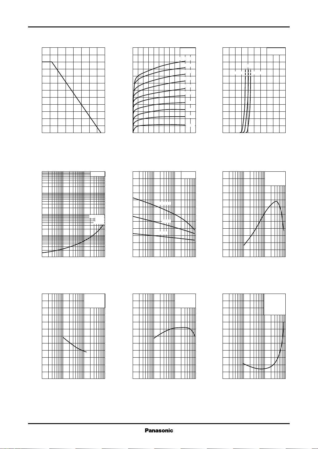
PC — Ta IC — V
240
)
mW
200
(
C
160
120
80
40
Collector power dissipation P
0
0 16040 12080 14020 10060
C
IC/IB=10
Ta=75˚C
25˚C
–25˚C
)
)
Ambient temperature Ta (˚C
V
— I
CE(sat)
)
100
V
(
30
CE(sat)
10
3
1
0.3
0.1
0.03
0.01
Collector to emitter saturation voltage V
0.1 1 10 1000.3 3 30
Collector current IC (mA
CE
24
20
)
mA
(
16
C
12
8
Collector current I
4
0
012108264
IB=200µA
Collector to emitter voltage VCE (V
hFE — I
C
600
FE
500
400
300
200
100
Forward current transfer ratio h
0
0.1 1 10 1000.3 3 30
Ta=75˚C
25˚C
–25˚C
Collector current IC (mA
Ta=25˚C
180µA
160µA
140µA
120µA
100µA
80µA
60µA
40µA
20µA
VCE=8V
)
120
100
)
mA
(
80
C
60
40
Collector current I
20
0
02.01.60.4 1.20.8
)
Base to emitter voltage VBE (V
12
)
10
GHz
(
T
8
6
4
2
Transition frequency f
0
0.1 1 10 1000.3 3 30
IC — V
BE
VCE=8V
25˚C
Ta=75˚C
–25˚C
fT — I
C
VCE=8V
f=800MHz
Ta=25˚C
Collector current IC (mA
)
)
)
pF
(
Cob — V
2.4
2.0
ob
1.6
1.2
0.8
0.4
CB
Collector output capacitance C
0
0.1 1 10 1000.3 3 30
Collector to base voltage VCB (V
2
IE=0
f=1MHz
Ta=25˚C
GUM — I
24
)
dB
(
20
16
12
8
4
Maximum unilateral power gain GUM
0
0.1 1 10 1000.3 3 30
)
Collector current IC (mA
C
VCE=8V
f=800MHz
Ta=25˚C
NF — I
C
)
dB
(
12
10
8
6
4
VCE=8V
=50Ω)
(R
g
f=800MHz
Ta=25˚C
Noise figure NF
2
0
0.1 10 100 10000.3 3 300
)
Collector current IC (mA
)
 Loading...