

Panasonic 2SC3611 Datasheet
Power Transistors
2SC3611
Silicon NPN epitaxial planar type
For video amplifier
■ Features
•
High transition frequency f
•
Small collector output capacitance C
•
Wide current range
•
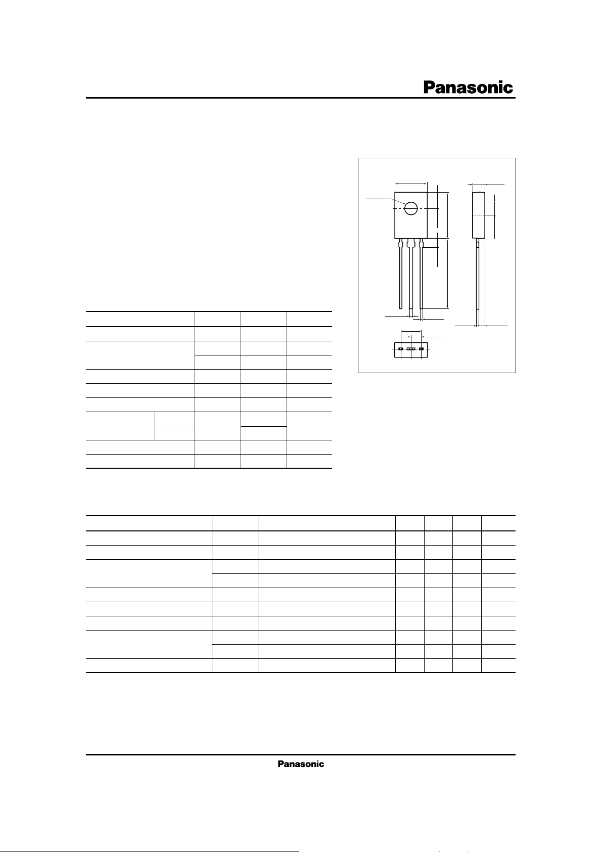
TO-126B package which requires no insulation plate for installation to the heat sink
T
ob
φ 3.16
±0.1
8.0
+0.5
–0.1
±0.3
3.8
±0.1
1.9
±0.5
11.0
±1.0
16.0
Unit: mm
3.2
±0.2
±0.1
3.05
■ Absolute Maximum Ratings TC = 25°C
Parameter Symbol Rating Unit
Collector to base voltage V
Collector to emitter voltage V
V
Emitter to base voltage V
Peak collector current I
Collector current I
Collector power
dissipation
TC = 25°CPC1.2 W
Ta = 25°C 4.0
Junction temperature T
Storage temperature T
CBO
CER
CEO
EBO
CP
C
j
stg
110 V
100 V
50 V
3.5 V
300 mA
150 mA
150 °C
−55 to +150 °C
Note)*: With a 100 × 100 × 2 mm A1 heat sink
■ Electrical Characteristics TC = 25°C
Parameter Symbol Conditions Min Typ Max Unit
Collector cutoff current I
Collector to base voltage V
Collector to emitter voltage V
Emitter to base voltage V
Forward current transfer ratio h
Collector to emitter saturation voltage
Transition frequency f
Collector output capacitance C
V
V
CEO
CBO
CER
CEO
EBO
FE
CE(sat)
T1
f
T2
ob
0.75
±0.1
0.5
±0.1
0.5
±0.1
4.6
±0.2
2.3
±0.2
123
TO-126B-A1 Package
*
1.76
1 : Base
2 : Collector
3 : Emitter
VCE = 35 V, IB = 0 10 µA
IC = 100 µA, IE = 0 110 V
IC = 500 µA, RBE = 470 Ω 100 V
IC = 1 mA, IB = 0 50 V
IE = 100 µA, IC = 0 3.5 V
VCE = 5 V, IC = 100 mA 20
IC = 150 mA, IB = 15 mA 0.5 V
VCB = 10 V, IE = −10 mA, f = 200 MHz
VCB = 10 V, IE = −110 mA, f = 200 MHz
300 MHz
350 MHz
VCB = 30 V, IE = 0, f = 1 MHz 3 pF
±0.1
201
2SC3611
Power Transistors
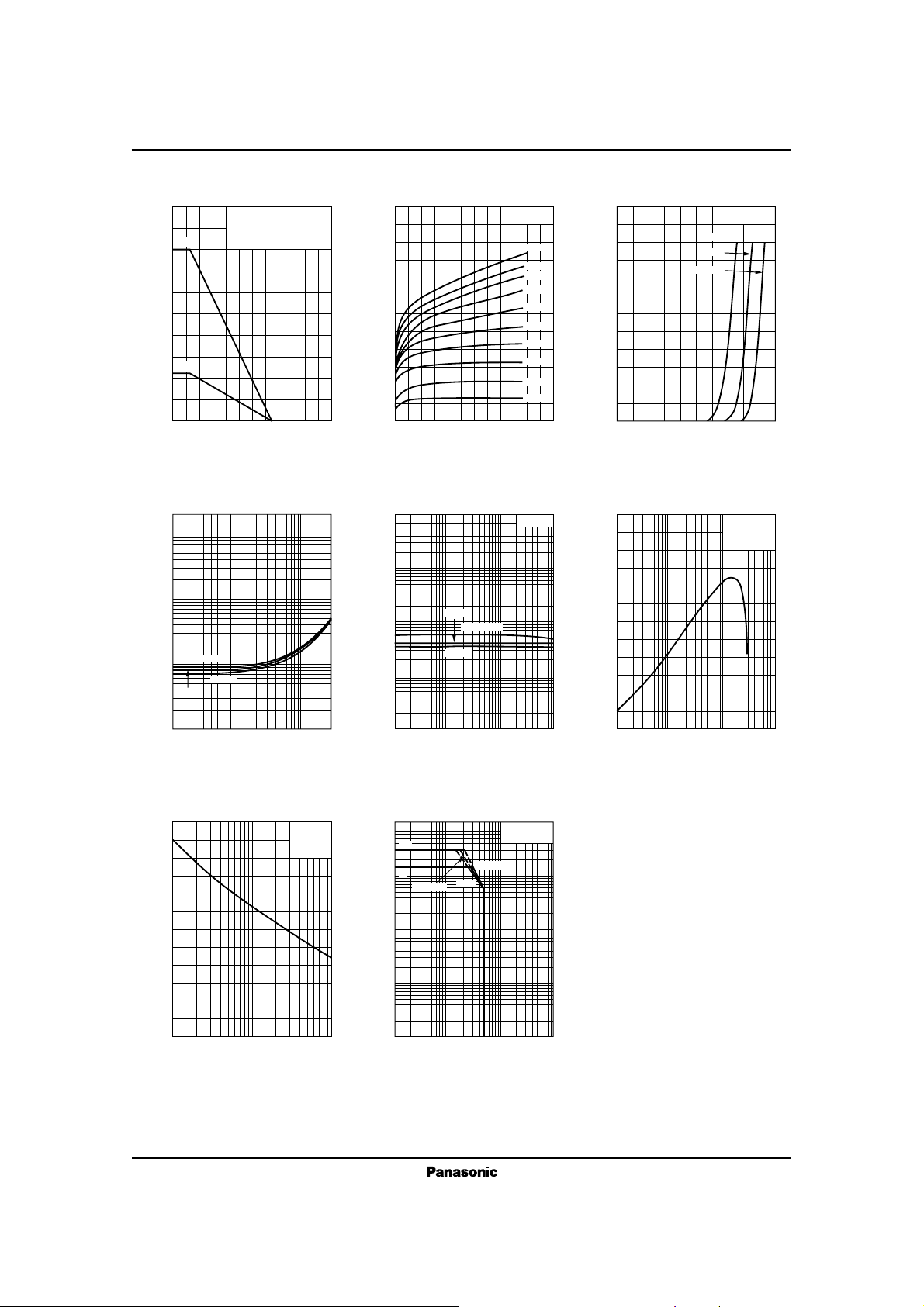
PC T
a
5
)
W
(
(1)
4
C
3
2
(2)
1
(1)With a 100×100×2mm
Al heat sink
(2)Without heat sink
Collector power dissipation P
0
0 24040 20080 160120
Ambient temperature Ta (˚C
V
I
)
V
(
10
CE(sat)
3
1
0.3
0.1
25˚C
0.03
0.01
Collector to emitter saturation voltage V
1310 30 100 300
CE(sat)
TC=100˚C
–25˚C
Collector current IC (mA
)
C
IC/IB=5
)
IC V
CE
240
200
)
mA
(
160
C
120
80
Collector current I
40
0
012210486
IB=5.0mA
Collector to emitter voltage VCE (V
hFE I
10000
3000
FE
1000
300
100
30
10
Forward current transfer ratio h
3
1
0.1 1100.3 3 30 100
25˚C
–25˚C
C
TC=100˚C
Collector current IC (mA
TC=25˚C
4.5mA
4.0mA
3.5mA
3.0mA
2.5mA
2.0mA
1.5mA
1.0mA
0.5mA
=5V
V
CE
)
120
100
)
mA
(
80
C
60
40
Collector current I
20
0
01.00.80.60.40.2
)
Base to emitter voltage VBE (V
600
)
500
MHz
(
T
400
300
200
100
Transition frequency f
0
–1 –3 –10 –30 –100 –300 –1000
IC V
BE
VCE=5V
TC=100˚C
25˚C
–25˚C
fT I
E
VCB=10V
f=200MHz
=25˚C
T
C
Emitter current IE (mA
)
)
Cob V
6
)
pF
(
5
ob
4
3
2
1
Collector output capacitance C
0
3 10 30 100
1
Collector to base voltage VCB (V
202
CB
IE=0
f=1MHz
=25˚C
T
C
1000
300
)
100
A
(
C
Collector current I
)
Area of safe operation (ASO)
Single pulse
=25˚C
T
I
CP
I
C
30
10
3
1
0.3
0.1
13
t=1s
t=100ms
10 30 100 300 1000
Collector to emitter voltage VCE (V
C
t=10ms
)
 Loading...