

Panasonic 2SC3314 Datasheet
Transistor
2SC3314
Silicon NPN epitaxial planer type
For high-frequency amplification
Complementary to 2SA1323
Features
■
●
Optimum for high-density mounting.
●
Allowing supply with the radial taping.
●
Optimum for RF amplification of FM/AM radios.
●
High transition frequency fT.
Absolute Maximum Ratings (Ta=25˚C)
■
Parameter
Collector to base voltage
Collector to emitter voltage
Emitter to base voltage
Collector current
Collector power dissipation
Junction temperature
Storage temperature
Symbol
V
CBO
V
CEO
V
EBO
I
C
P
C
T
j
T
stg
Ratings
–55 ~ +150
30
20
30
300
150
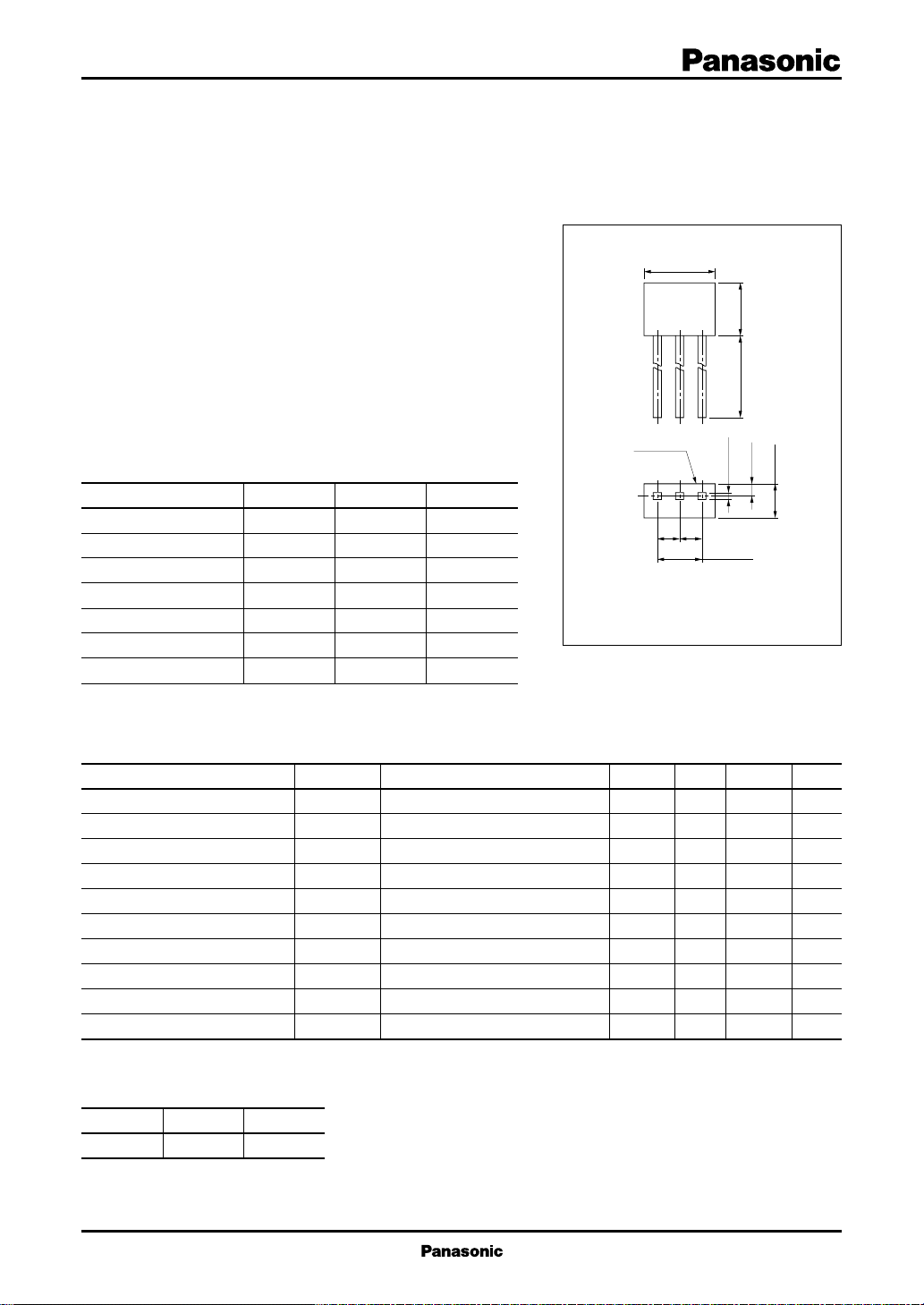
Unit: mm
4.0±0.2
3.0±0.215.6±0.5
marking
123
+0.2
0.1
–
0.45
0.7±0.1
2.0±0.2
Unit
V
V
5
V
mA
mW
1:Emitter
2:Collector EIAJ:SC–72
3:Base New S Type Package
1.271.27
2.54±0.15
˚C
˚C
Electrical Characteristics (Ta=25˚C)
■
Parameter
Collector to base voltage
Collector to emitter voltage
Emitter to base voltage
Forward current transfer ratio
Collector to emitter saturation voltage
Base to emitter voltage
Transition frequency
Noise figure
Common emitter reverse transfer capacitance
Reverse transfer impedance
*
hFE Rank classification
Symbol
V
CBO
V
CEO
V
EBO
h
FE
V
CE(sat)
V
BE
f
T
NF
C
re
Z
rb
Rank B C
h
FE
70 ~ 140 110 ~ 220
Conditions
IC = 10µA, IE = 0
IC = 1mA, IB = 0
IE = 10µA, IC = 0
*
VCE = 10V, IC = 1mA
IC = 10mA, IB = 1mA
VCE = 10V, IC = 1mA
VCB = 10V, IE = –1mA, f = 200MHz
VCB = 10V, IE = –1mA, f = 5MHz
VCE = 10V, IC = 1mA, f = 10.7MHz
VCB = 10V, IE = –1mA, f = 2MHz
min
30
20
5
70
150
typ
0.1
0.7
300
2.8
max
220
4.0
1.5
50
Unit
V
V
V
V
V
MHz
dB
pF
Ω
1
Transistor
2SC3314
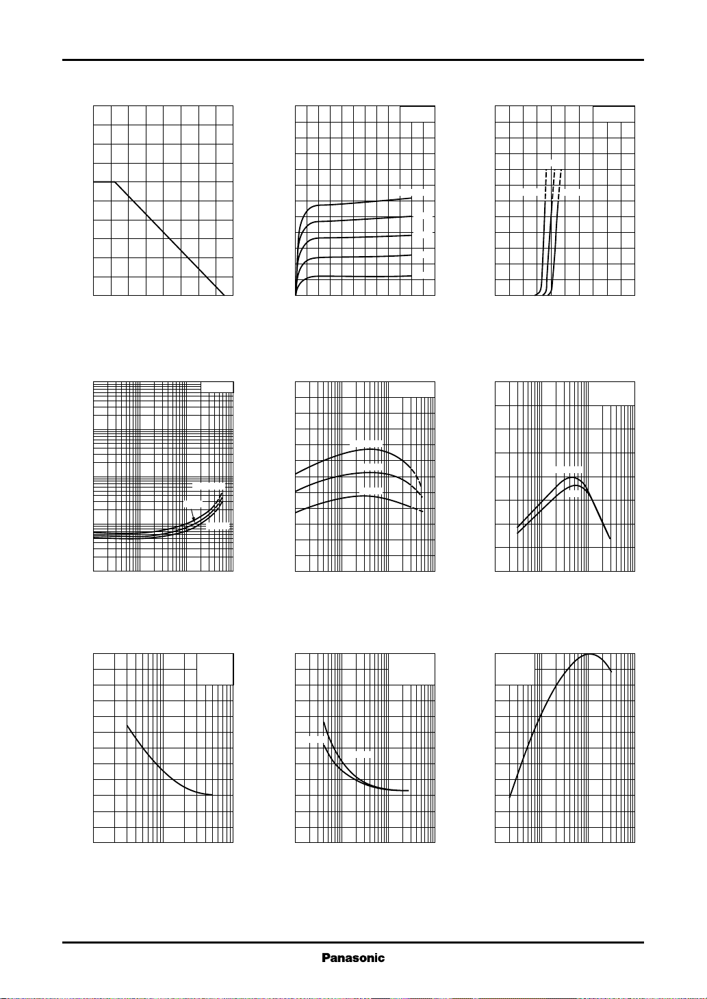
PC — Ta IC — V
500
)
mW
(
400
C
300
200
100
Collector power dissipation P
0
0 16040 12080 14020 10060
Ambient temperature Ta (˚C
V
— I
CE(sat)
)
100
V
(
30
CE(sat)
10
3
1
0.3
0.1
0.03
0.01
Collector to emitter saturation voltage V
0.1 1 10 1000.3 3 30
25˚C
Collector current IC (mA
)
C
IC/IB=10
Ta=75˚C
–25˚C
)
CE
240
200
)
mA
(
160
C
120
80
Collector current I
40
0
012108264
IB=100µA
Collector to emitter voltage VCE (V
hFE — I
C
240
FE
200
160
120
80
40
Forward current transfer ratio h
0
0.1 1 10 1000.3 3 30
Ta=75˚C
VCE=10V
25˚C
–25˚C
Collector current IC (mA
Ta=25˚C
80µA
60µA
40µA
20µA
)
60
50
)
mA
(
40
C
30
20
Collector current I
10
0
02.01.60.4 1.20.8
)
Base to emitter voltage VBE (V
800
700
)
MHz
600
(
T
500
400
300
200
Transition frequency f
100
0
– 0.1 –1 –10 –100– 0.3 –3 –30
IC — V
BE
VCE=10V
25˚C
Ta=75˚C
fT — I
VCE=10V
–25˚C
E
Ta=25˚C
6V
Emitter current IE (mA
)
)
Zrb — I
E
60
)
Ω
(
50
rb
40
30
20
10
Reverse transfer impedance Z
0
– 0.1 – 0.3 –1 –3 –10
Emitter current IE (mA
2
VCB=10V
f=2MHz
Ta=25˚C
)
Cre — V
)
3.0
pF
(
re
2.5
2.0
1mA
1.5
1.0
0.5
Common emitter reverse transfer capacitance C
0
0.1 1 10 1000.3 3 30
Collector to emitter voltage VCE (V
IC=3mA
CE
f=10.7MHz
Ta=25˚C
)
PG — I
E
24
VCE=10V
f=100MHz
Ta=25˚C
20
)
dB
(
16
12
8
Power gain PG
4
0
– 0.1 –1 –10 –100– 0.3 –3 –30
Emitter current IE (mA
)
 Loading...