


Panasonic 2SB1209 Datasheet
Transistor
2SB1209
Silicon PNP triple diffusion planer type
For low-frequency amplification
Features
■
●
High collector to base voltage V
●
High collector to emitter voltage V
●
Low collector to emitter saturation voltage V
Absolute Maximum Ratings (Ta=25˚C)
■
Parameter
Collector to base voltage
Collector to emitter voltage
Emitter to base voltage
Peak collector current
Collector current
Collector power dissipation
Junction temperature
Storage temperature
*
Printed circuit board: Copper foil area of 1cm2 or more, and the board
thickness of 1.7mm for the collector portion
Symbol
V
V
V
I
CP
I
C
P
C
T
j
T
stg
CBO
CEO
EBO
*
CBO
CEO
.
.
Ratings
–400
–400
–5
–200
–100
1
150
–55 ~ +150
CE(sat)
.
Unit
V
V
V
mA
mA
W
˚C
˚C
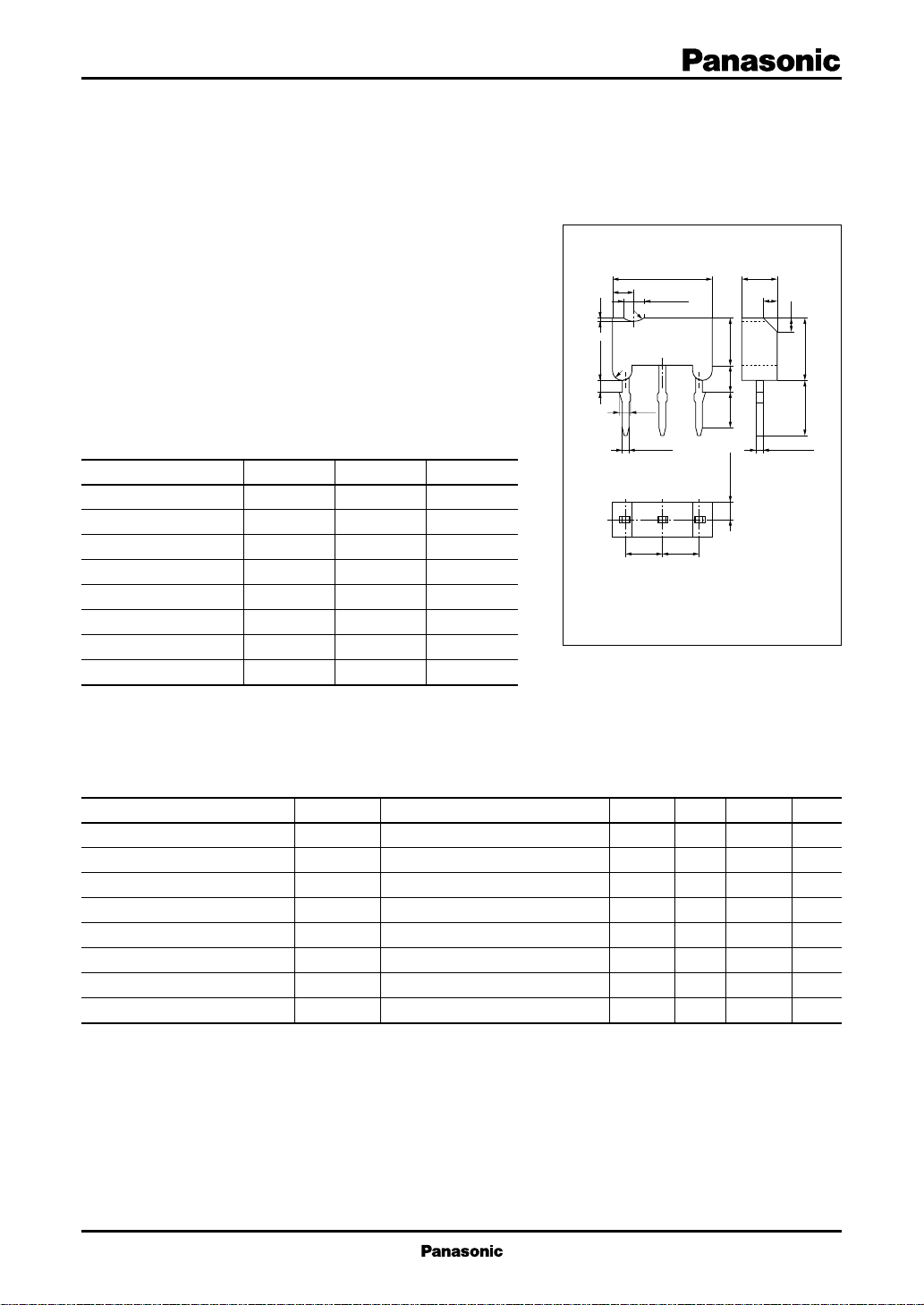
6.9±0.1
1.5
1.5 R0.9
0.4
R0.9
R0.7
1.0±0.1
0.85
0.55±0.1 0.45±0.05
2.5 2.5
1:Base
2:Collector EIAJ:SC–71
3:Emitter M Type Mold Package
2.5±0.1
1.0
3.5±0.1
2.0±0.2
2.4±0.21.25±0.05
123
Unit: mm
1.0
4.1±0.2 4.5±0.1
Electrical Characteristics (Ta=25˚C)
■
Parameter
Collector to base voltage
Collector to emitter voltage
Emitter to base voltage
Forward current transfer ratio
Collector to emitter saturation voltage
Base to emitter saturation voltage
Transition frequency
Collector output capacitance
Symbol
V
CBO
V
CEO
V
EBO
h
FE
V
CE(sat)
V
BE(sat)
f
T
C
ob
Conditions
IC = –100µA, IE = 0
IC = –500µA, IB = 0
IE = –100µA, IC = 0
VCE = –5V, IC = –30mA
IC = –10mA, IB = –1mA
IC = –50mA, IB = –5mA
VCB = –30V, IE = 20mA, f = 200MHz
VCB = –30V, IE = 0, f = 1MHz
min
–400
–400
–5
40
typ50max
– 0.6
–1.5
9
Unit
V
V
V
V
V
MHz
pF
1
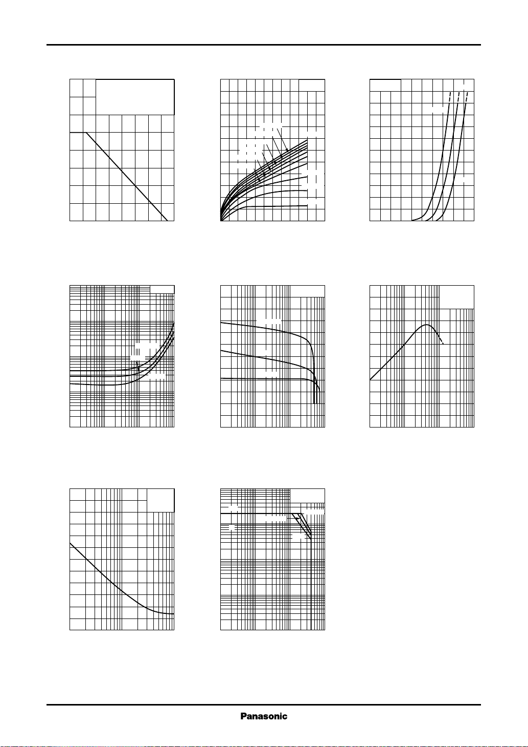
Transistor 2SB1209
PC — Ta IC — V
1.6
)
1.4
W
(
C
1.2
1.0
0.8
0.6
0.4
0.2
Collector power dissipation P
0
)
–100
V
(
–30
CE(sat)
–10
–3
–1
– 0.3
– 0.1
– 0.03
– 0.01
Collector to emitter saturation voltage V
– 0.1 –1 –10 –100– 0.3 –3 –30
Printed circut board: Copper
foil area of 1cm
the board thickness of 1.7mm
for the collector portion.
0 16040 12080 14020 10060
2
or more, and
Ambient temperature Ta (˚C
V
— I
CE(sat)
C
IC/IB=10
TC=75˚C
25˚C
–25˚C
Collector current IC (mA
)
)
CE
–120
–100
)
mA
(
–80
C
–60
–40
Collector current I
–20
0
0 –12–10–8–2 –6–4
– 0.6mA
– 0.5mA
– 0.4mA
– 0.8mA
– 0.7mA
– 0.9mA
Collector to emitter voltage VCE (V
hFE — I
C
240
FE
200
Ta=75˚C
160
120
80
40
Forward current transfer ratio h
0
– 0.1 –1 –10 –100– 0.3 –3 –30
25˚C
–25˚C
VCE=–5V
Collector current IC (mA
Ta=25˚C
IB=–1mA
– 0.3mA
– 0.2mA
– 0.1mA
)
–120
–100
)
mA
(
–80
C
–60
–40
Collector current I
–20
0
0 –1.0– 0.8– 0.2 – 0.6– 0.4
)
Base to emitter voltage VBE (V
120
)
100
MHz
(
T
80
60
40
20
Transition frequency f
0
1 10 100 10003 30 300
IC — V
BE
VCE=–5V
Ta=75˚C
fT — I
E
Emitter current IE (mA
25˚C
–25˚C
VCB=–30V
=25˚C
T
C
)
)
)
pF
(
Cob — V
30
25
ob
20
15
10
5
CB
Collector output capacitance C
0
1 3 10 30 100
Collector to base voltage VCB (V
2
IE=0
f=1MHz
Ta=25˚C
)
Area of safe operation (ASO)
–1000
–300
I
CP
)
–100
A
(
I
C
C
–30
–10
–3
–1
Collector current I
– 0.3
– 0.1
–1 –10 –100 –1000–3 –30 –300
Collector to emitter voltage VCE (V
t=100ms
Single pulse
Ta=25˚C
t=1s
t=10ms
)