

Panasonic 2SB1030A, 2SB1030 Datasheet
Transistor
2SB1030, 2SB1030A
Silicon PNP epitaxial planer type
For low-frequency amplification
Complementary to 2SD1423 and 2SD1423A
Features
■
●
Optimum for high-density mounting.
●
Allowing supply with the radial taping.
Absolute Maximum Ratings (Ta=25˚C)
■
Parameter
Collector to
base voltage
Collector to
emitter voltage
2SB1030
2SB1030A
2SB1030
2SB1030A
Emitter to base voltage
Peak collector current
Collector current
Collector power dissipation
Junction temperature
Storage temperature
Electrical Characteristics (Ta=25˚C)
■
Parameter
Collector cutoff current
Collector to base
voltage
Collector to emitter
voltage
Emitter to base voltage
Forward current transfer ratio
Collector to emitter saturation voltage
Transition frequency
Collector output capacitance
*1
h
Rank classification
FE1
Rank Q R S
h
FE1
85 ~ 170 120 ~ 240 170 ~ 340
Symbol
2SB1030
2SB1030A
2SB1030
2SB1030A
Ratings
V
CBO
V
CEO
V
EBO
I
CP
I
C
P
C
T
j
T
stg
–30
–60
–25
–50
–7
–1
– 0.5
300
150
–55 ~ +150
Symbol
I
I
V
V
V
h
h
V
f
C
CBO
CEO
FE1
FE2
T
CBO
CEO
EBO
*1
CE(sat)
ob
VCB = –20V, IE = 0
VCE = –20V, IB = 0
IC = –10µA, IE = 0
IC = –2mA, IB = 0
IE = –10µA, IC = 0
VCE = –10V, IC = –150mA
VCE = –10V, IC = –500mA
IC = –300mA, IB = –30mA
VCB = –10V, IE = 50mA, f = 200MHz
VCB = –10V, IE = 0, f = 1MHz
Unit
V
V
V
A
A
mW
˚C
˚C
Conditions
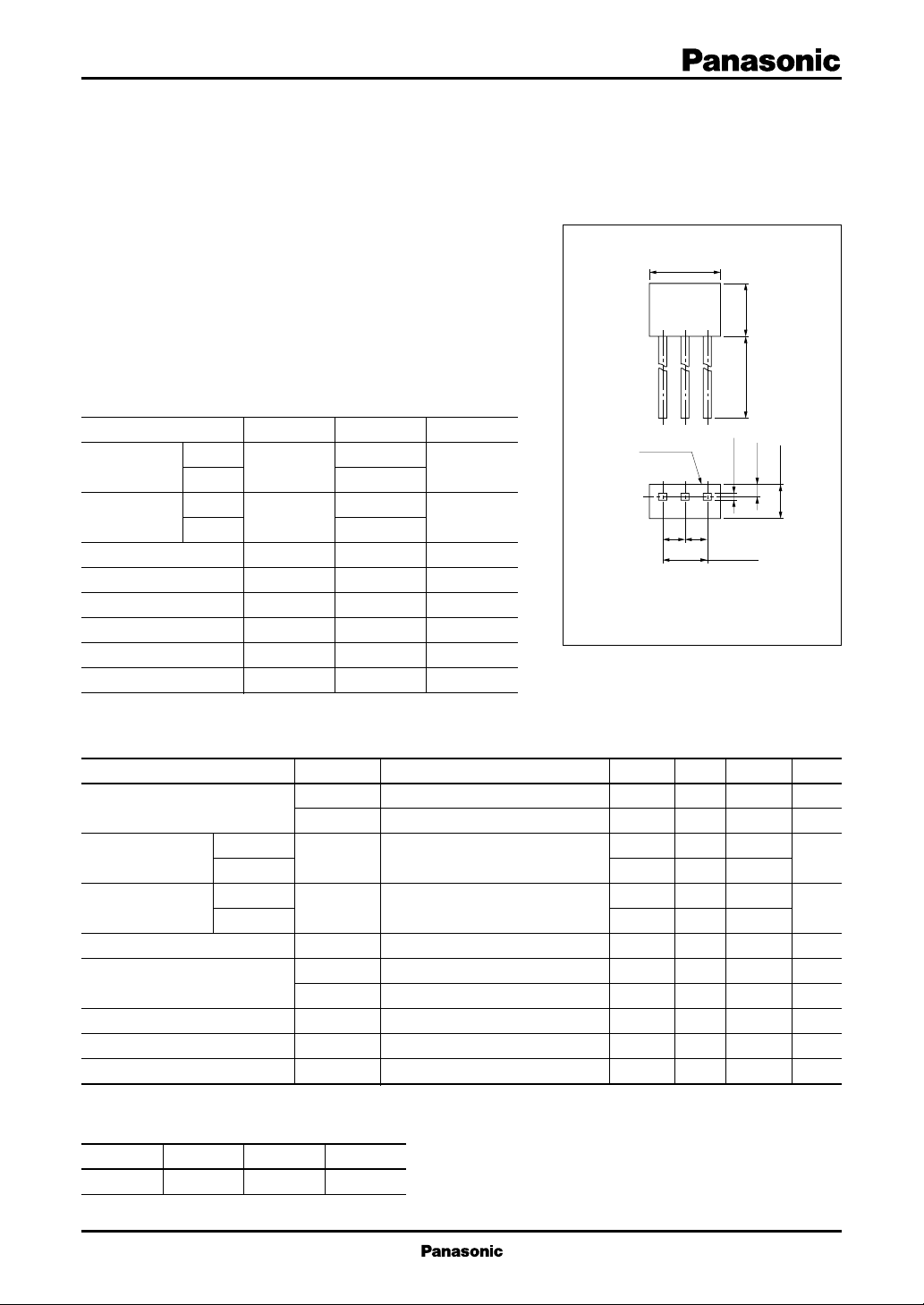
4.0±0.2
marking
123
1.271.27
1:Emitter
2:Collector EIAJ:SC–72
3:Base New S Type Package
min
typ
–30
–60
–25
–50
–7
*2
*2
*2
85
40
– 0.35
200
3.0±0.215.6±0.5
0.1
+0.2
–
0.7±0.1
0.45
2.54±0.15
max
– 0.1
–1
340
– 0.6
6
15
*2
Pulse measurement
Unit: mm
2.0±0.2
Unit
µA
µA
V
V
V
V
MHz
pF
1
Transistor
2SB1030, 2SB1030A
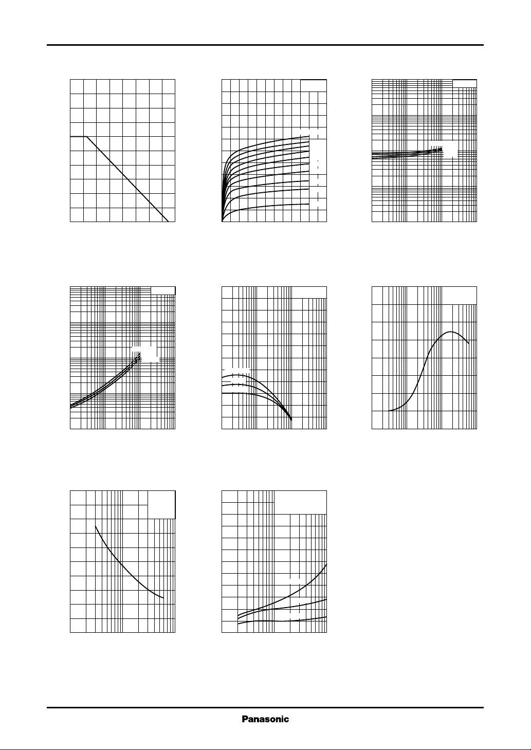
PC — Ta IC — V
500
)
450
mW
(
400
C
350
300
250
200
150
100
50
Collector power dissipation P
0
0 16040 12080 14020 10060
C
25˚C
–25˚C
)
IC/IB=10
)
Ambient temperature Ta (˚C
V
— I
CE(sat)
)
–100
V
(
–30
CE(sat)
–10
–3
–1
– 0.3
– 0.1
– 0.03
– 0.01
Collector to emitter saturation voltage V
– 0.01
– 0.1 –1 –10
– 0.03
Ta=75˚C
– 0.3 –3
Collector current IC (A
CE
–1200
–1000
)
mA
(
–800
C
–600
–400
Collector current I
–200
0
0 –12–10–8–2 –6–4
IB=–10mA
Collector to emitter voltage VCE (V
hFE — I
C
600
FE
500
400
300
Ta=75˚C
25˚C
200
–25˚C
100
Forward current transfer ratio h
0
– 0.01
– 0.1 –1 –10
– 0.03
VCE=–10V
– 0.3 –3
Collector current IC (A
Ta=25˚C
–9mA
–8mA
–7mA
–6mA
–5mA
–4mA
–3mA
–2mA
–1mA
)
V
BE(sat)
–100
)
V
(
–30
BE(sat)
–10
–3
–1
– 0.3
– 0.1
– 0.03
Base to emitter saturation voltage V
– 0.01
– 0.01
)
– 0.1 –1 –10
– 0.03
– 0.3 –3
Collector current IC (A
fT — I
160
140
)
MHz
120
(
T
100
80
60
40
Transition frequency f
20
0
0.1 1 10 1000.3 3 30
Emitter current IE (mA
— I
E
C
Ta=–25˚C
25˚C
75˚C
VCB=–10V
Ta=25˚C
IC/IB=10
)
)
Cob — V
20
)
18
pF
(
16
ob
14
12
10
8
6
4
2
Collector output capacitance C
0
–1 –3 –10 –30 –100
CB
Collector to base voltage VCB (V
2
IE=0
f=1MHz
Ta=25˚C
)
mV
(
Noise voltage NV
)
NV — I
C
240
200
160
120
80
40
0
–10 –30 –100 –300 –1000
VCE=–10V
Ta=25˚C
Function=FLAT
Rg=100kΩ
22kΩ
4.7kΩ
Collector current IC (µA
)
 Loading...