

Panasonic 2SB0970 Datasheet
Transistor
2.8
+0.2
–0.3
1.5
+0.25
–0.050.65±0.15 0.65±0.15
3
1
2
0.950.95
1.9±0.2
0.4
+0.1
–0.05
1.1
+0.2
–0.1
0.8
0.4±0.2
0 to 0.1
0.16
+0.1
–0.06
1.45
0.1 to 0.3
2.9
+0.2
–0.05
2SB970
Silicon PNP epitaxial planer type
For low-voltage output amplification
Features
■
●
Low collector to emitter saturation voltage V
●
Mini type package, allowing downsizing of the equipment and
automatic insertion through the tape packing and the magazine
packing.
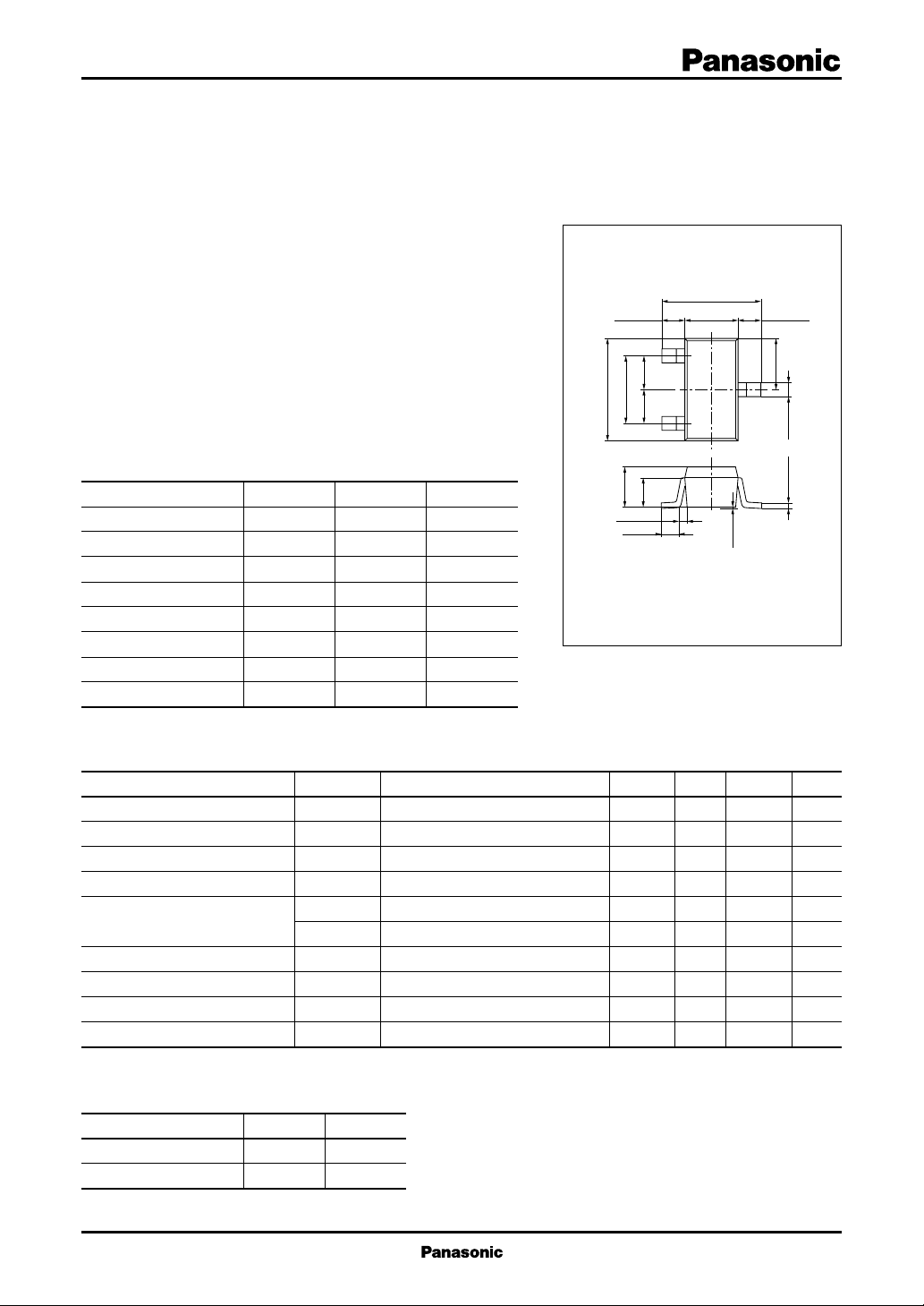
Absolute Maximum Ratings (Ta=25˚C)
■
Parameter
Collector to base voltage
Collector to emitter voltage
Emitter to base voltage
Peak collector current
Collector current
Collector power dissipation
Junction temperature
Storage temperature
Symbol
V
CBO
V
CEO
V
EBO
I
CP
I
C
P
C
T
j
T
stg
Ratings
–15
–10
–7
–1
– 0.5
200
150
–55 ~ +150
CE(sat)
.
Unit
V
V
V
A
A
mW
˚C
˚C
Unit: mm
1:Base JEDEC:TO–236
2:Emitter EIAJ:SC–59
3:Collector Mini T ype Package
Marking symbol : 1R
Electrical Characteristics (Ta=25˚C)
■
Parameter
Collector cutoff current
Collector to base voltage
Collector to emitter voltage
Emitter to base voltage
Forward current transfer ratio
Collector to emitter saturation voltage
Base to emitter saturation voltage
Transition frequency
Collector output capacitance
*1
h
Rank classification
FE1
Rank R S
h
FE1
Marking Symbol 1RR 1RS
Symbol
I
CBO
V
CBO
V
CEO
V
EBO
*1
h
FE1
h
FE2
V
CE(sat)
V
BE(sat)
f
T
C
ob
130 ~ 220 180 ~ 350
Conditions
VCB = –10V, IE = 0
IC = –10µA, IE = 0
IC = –1mA, IB = 0
IE = –10µA, IC = 0
VCE = –2V, IC = –0.5A
VCE = –2V, IC = –1A
*2
*2
IC = –0.4A, IB = –8mA
IC = –0.4A, IB = –8mA
VCB = –10V, IE = 50mA, f = 200MHz
VCB = –10V, IE = 0, f = 1MHz
min
–15
–10
–7
130
60
typ
– 0.16
– 0.8
130
22
*2
Pulse measurement
max
–100
350
– 0.3
–1.2
Unit
nA
V
V
V
V
V
MHz
pF
1
Transistor
2SB970
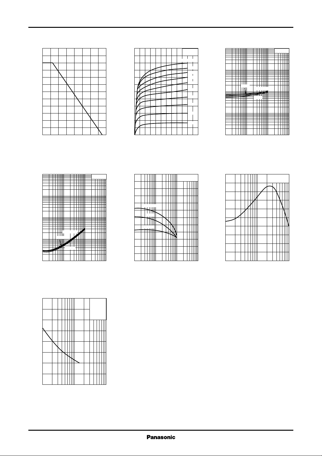
PC — Ta IC — V
240
)
mW
200
(
C
160
120
80
40
Collector power dissipation P
0
0 16040 12080 14020 10060
Ambient temperature Ta (˚C
V
— I
CE(sat)
)
–100
V
(
–30
CE(sat)
–10
–3
–1
– 0.3
– 0.1
– 0.03
– 0.01
Collector to emitter saturation voltage V
– 0.01
Ta=75˚C
25˚C
–25˚C
– 0.1 –1 –10
– 0.03
– 0.3 –3
Collector current IC (A
)
C
IC/IB=50
)
CE
–1.2
IB=–10mA
)
A
(
–1.0
– 0.8
C
– 0.6
– 0.4
Collector current I
– 0.2
0
0–6–5–4–1 –3–2
Collector to emitter voltage VCE (V
hFE — I
C
600
FE
500
400
Ta=75˚C
25˚C
300
–25˚C
200
100
Forward current transfer ratio h
0
– 0.01
– 0.1 –1 –10
– 0.03
VCE=–2V
– 0.3 –3
Collector current IC (A
Ta=25˚C
–9mA
–8mA
–7mA
–6mA
–5mA
–4mA
–3mA
–2mA
–1mA
)
V
BE(sat)
–100
)
V
(
–30
BE(sat)
–10
–3
–1
– 0.3
– 0.1
– 0.03
Base to emitter saturation voltage V
– 0.01
– 0.01
)
25˚C
– 0.1 –1 –10
– 0.03
– 0.3 –3
Collector current IC (A
fT — I
200
180
)
160
MHz
(
140
T
120
100
80
60
40
Transition frequency f
20
0
1 3 10 30 100
Emitter current IE (mA
— I
Ta=–25˚C
75˚C
E
C
VCB=–10V
Ta=25˚C
IC/IB=50
)
)
Cob — V
80
)
pF
70
(
ob
60
50
40
30
20
10
Collector output capacitance C
0
–1 –3 –10 –30 –100
CB
Collector to base voltage VCB (V
2
IE=0
f=1MHz
Ta=25˚C
)
 Loading...