

Panasonic 2SB0936A, 2SB0936 Datasheet
Po wer Transistors
2SB936, 2SB936A
Silicon PNP epitaxial planar type
For low-voltage switching
Features
■
●
Low collector to emitter saturation voltage V
●
High-speed switching
●
N type package enabling direct soldering of the radiating fin to
the printed circuit board, etc. of small electronic equipment.
Absolute Maximum Ratings (T
■
Parameter
Collector to
base voltage
Collector to
emitter voltage
2SB936
2SB936A
2SB936
2SB936A
Emitter to base voltage
Peak collector current
Collector current
Collector power
dissipation
TC=25°C
Ta=25°C
Junction temperature
Storage temperature
Electrical Characteristics (T
■
Parameter
Collector cutoff
current
Emitter cutoff current
Collector to emitter
voltage
Forward current transfer ratio
Collector to emitter saturation voltage
Base to emitter saturation voltage
Transition frequency
Collector output capacitance
Turn-on time
Storage time
Fall time
*
h
Rank classification
FE2
Rank Q P
h
FE2
90 to 180 130 to 260
Symbol
2SB936
2SB936A
2SB936
2SB936A
V
CBO
V
CEO
V
EBO
I
CP
I
C
P
C
T
j
T
stg
=25˚C)
C
Symbol
I
CBO
I
EBO
V
CEO
h
FE1
*
h
FE2
V
CE(sat)
V
BE(sat)
f
T
C
ob
t
on
t
stg
t
f
CE(sat)
=25˚C)
C
Ratings
–40
–50
–20
–40
–5
–20
–10
40
1.3
150
–55 to +150
VCB = –40V, IE = 0
VCB = –50V, IE = 0
VEB = –5V, IC = 0
IC = –10mA, IB = 0
VCE = –2V, IC = – 0.1A
VCE = –2V, IC = –3A
IC = –10A, IB = – 0.33A
IC = –10A, IB = – 0.33A
VCE = –10V, IC = – 0.5A, f = 10MHz
VCB = –10V, IE = 0, f = 1MHz
IC = –3A, IB1 = – 0.1A, IB2 = 0.1A
Unit
V
V
V
A
A
W
˚C
˚C
Conditions
10.0±0.310.5min.
10.0±0.3
2.0
4.4±0.5
2.0 1.5±0.1
123
8.5±0.2
6.0±0.5
5.08±0.5
213
8.5±0.2
6.0±0.3
5.08±0.5
min
–20
–40
45
90
1.5max.
0.8±0.1
2.54±0.3
0.8±0.1
2.54±0.3
–0.4
+0
1.5
R0.5
R0.5
1.1 max.
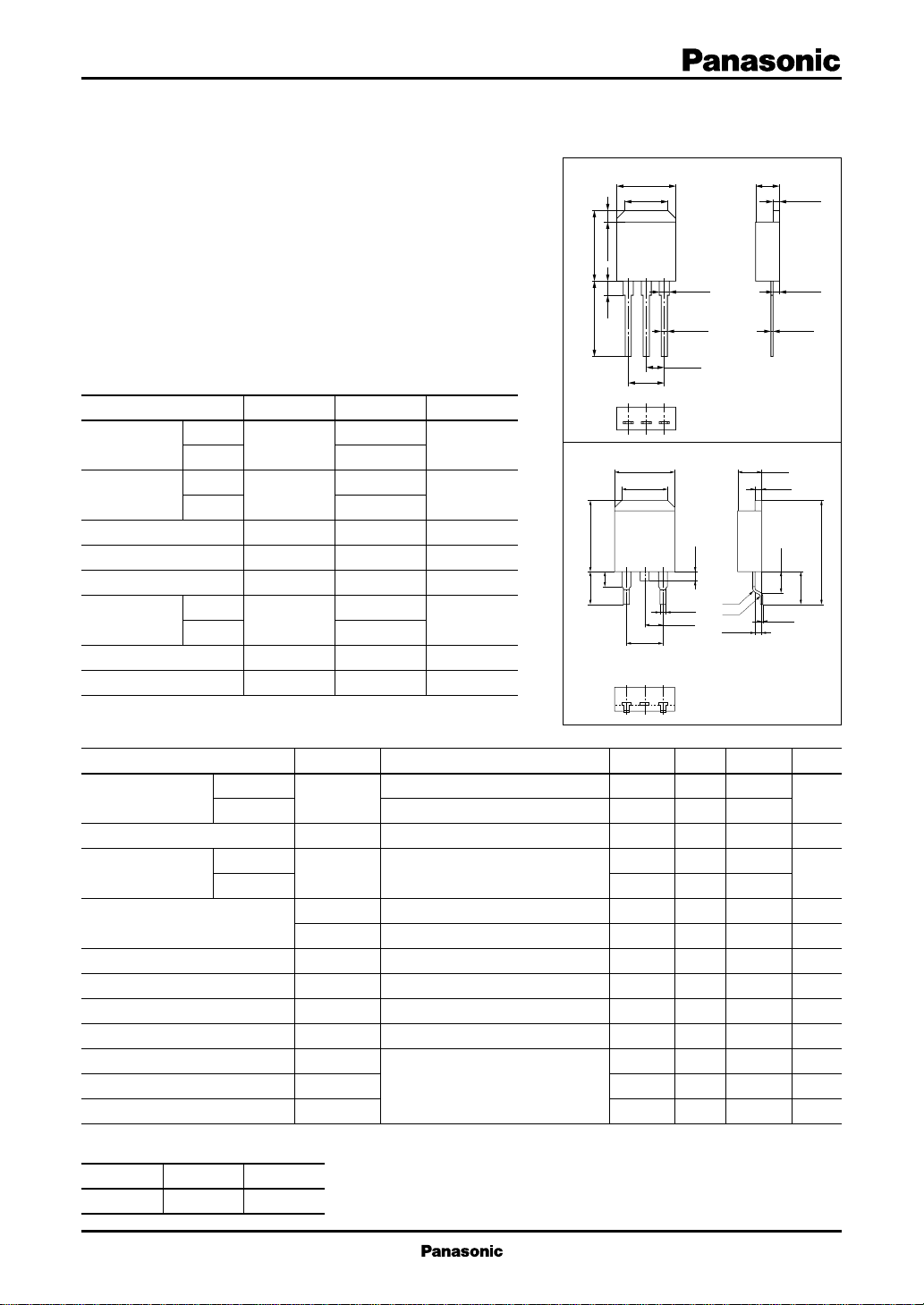
1:Base
2:Collector
3:Emitter
N Type Package (DS)
typ
max
– 0.6
–1.5
100
400
0.1
0.5
0.1
Unit: mm
3.4±0.3
1.0±0.1
1.1max.
0.5max.
1:Base
2:Collector
3:Emitter
N Type Package
Unit: mm
3.4±0.3
1.0±0.1
–0.2
+0.4
3.0
4.4±0.5
0 to 0.4
Unit
–50
–50
–50
µA
µA
V
260
V
V
MHz
pF
µs
µs
µs
14.7±0.5
1
Po wer Transistors 2SB936, 2SB936A
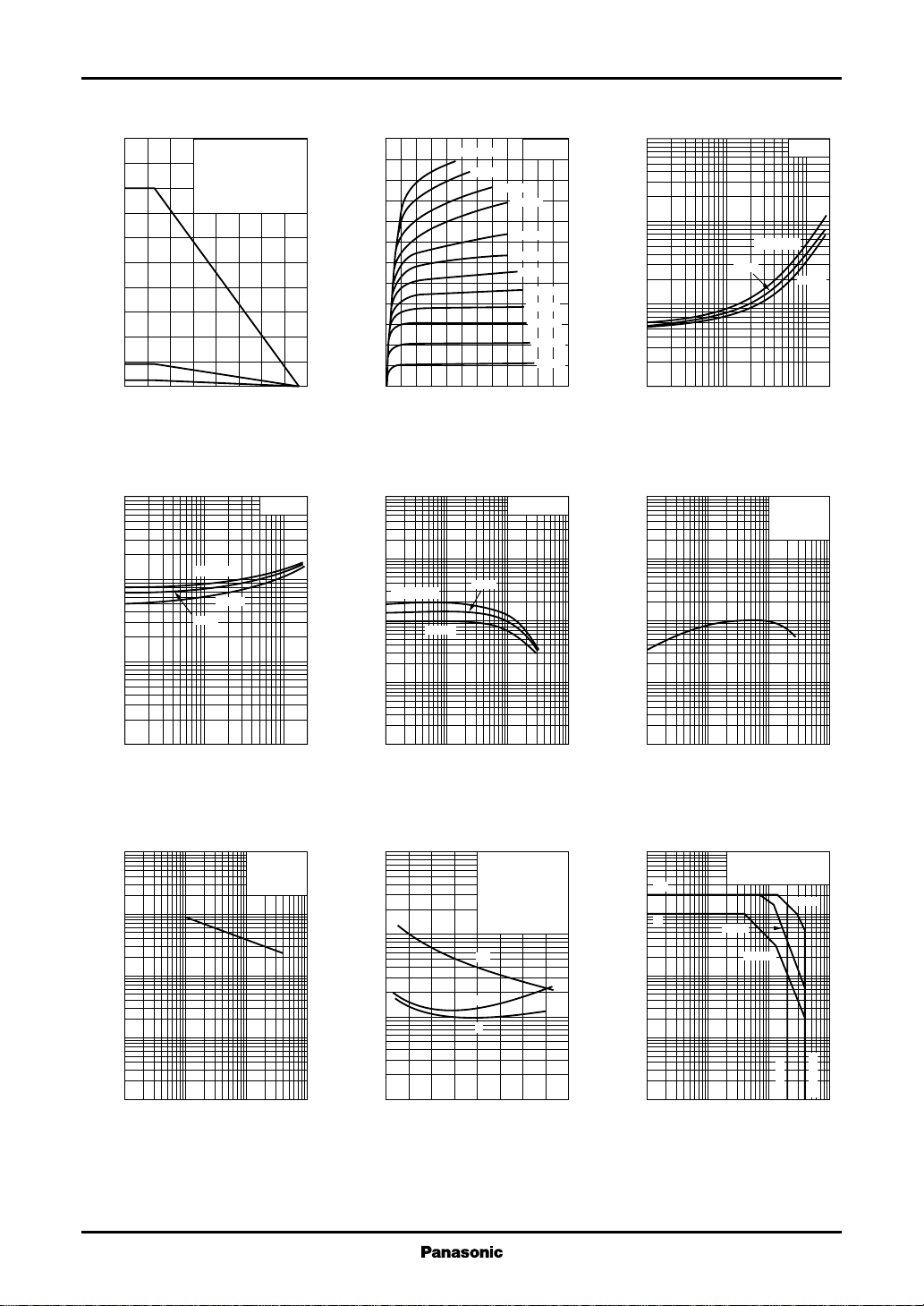
PC—Ta IC—V
50
)
W
(
(1)
40
C
30
20
10
(2)
Collector power dissipation P
(3)
0
0 16040 12080 14020 10060
Ambient temperature Ta (˚C
–10
)
V
(
–3
BE(sat)
–1
– 0.3
– 0.1
– 0.03
Base to emitter saturation voltage V
– 0.01
– 0.1 –1 –10– 0.3 –3
(1) TC=Ta
(2) With a 50 × 50 × 2mm
Al heat sink
(3) Without heat sink
(P
=1.3W)
C
V
BE(sat)—IC
IC/IB=30
TC=–25˚C
100˚C
25˚C
Collector current IC (A
)
CE
)
–12
–10
)
A
(
–8
C
–6
–4
IB=–100mA
–80mA
Collector current I
–2
0
0 –12–10–8–2 –6–4
)
Collector to emitter voltage VCE (V
hFE—I
10000
3000
FE
1000
300
TC=100˚C
100
30
10
Forward current transfer ratio h
–25˚C
3
1
– 0.1 –1 –10 –100– 0.3 –3 –30
Collector current IC (A
TC=25˚C
–60mA
–50mA
–40mA
–35mA
–30mA
–25mA
–20mA
–15mA
–10mA
–5mA
C
VCE=–2V
25˚C
)
–10
V
(
–3
CE(sat)
–1
– 0.3
– 0.1
– 0.03
– 0.01
Collector to emitter saturation voltage V
)
10000
3000
)
MHz
1000
(
T
300
100
30
10
Transition frequency f
V
CE(sat)—IC
TC=100˚C
25˚C
– 0.1 –1 –10– 0.3 –3
Collector current IC (A
fT—I
C
3
1
– 0.01
– 0.1 –1 –10
– 0.03
– 0.3 –3
Collector current IC (A
IC/IB=30
–25˚C
)
VCE=–10V
f=10MHz
T
=25˚C
C
)
Cob—V
10000
)
pF
3000
(
ob
1000
300
100
30
10
3
Collector output capacitance C
1
– 0.1 –1 –10 –100– 0.3 –3 –30
Collector to base voltage VCB (V
2
CB
IE=0
f=1MHz
=25˚C
T
C
)
ton, t
10
)
3
µs
(
f
,t
1
stg
,t
on
0.3
0.1
Switching time t
0.03
0.01
0–8–2 –6–4 –7–1 –5–3
Collector current IC (A
, tf — I
stg
t
on
C
Pulsed tw=1ms
Duty cycle=1%
=30
I
C/IB
(–I
B1=IB2
V
=–20V
CC
=25˚C
T
C
t
stg
t
f
Area of safe operation (ASO)
–100
–30
I
)
)
CP
)
–10
A
(
I
C
C
–3
–1
– 0.3
– 0.1
Collector current I
– 0.03
– 0.01
– 0.1 –1 –10 –100– 0.3 –3 –30
Collector to emitter voltage VCE (V
Non repetitive pulse
=25˚C
T
C
10ms
300ms
2SB936
t=1ms
2SB936A
)
 Loading...