

Panasonic 2SB0767 Datasheet
Transistor
2SB767
Silicon PNP epitaxial planer type
For low-frequency output amplification
Complementary to 2SD875
Features
■
●
Large collector power dissipation PC.
●
High collector to emitter voltage V
●
Mini type package, allowing downsizing of the equipment and
automatic insertion through the tape packing and the magazine
packing.
Absolute Maximum Ratings (Ta=25˚C)
■
Parameter
Collector to base voltage
Collector to emitter voltage
Emitter to base voltage
Peak collector current
Collector current
Collector power dissipation
Junction temperature
Storage temperature
*
Printed circuit board: Copper foil area of 1cm2 or more, and the board
thickness of 1.7mm for the collector portion
Symbol
V
CBO
V
CEO
V
EBO
I
CP
I
C
*
P
C
T
j
T
stg
.
CEO
Ratings
– 0.5
–55 ~ +150
Unit
–80
–80
–5
–1
1
150
V
V
V
A
A
W
˚C
˚C
0.4max.1.0
–0.2
+0.25
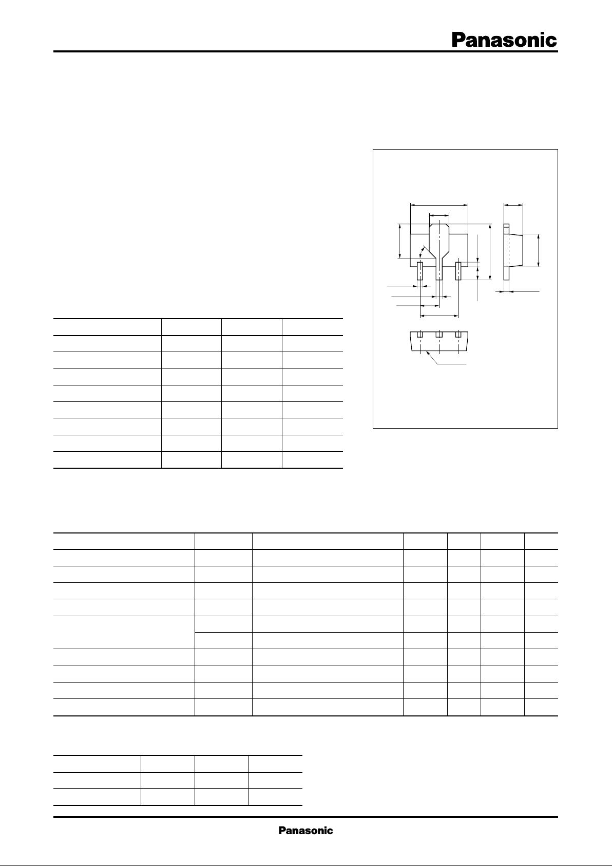
1.5±0.1
–0.20
4.0
4.5±0.1
1.6±0.2
2.6±0.1
45°
0.4±0.08
0.5±0.08
1.5±0.1
3.0±0.15
321
1:Base
2:Collector EIAJ:SC–62
3:Emitter Mini Power Type Package
+0.1
marking
Marking symbol : C
Unit: mm
2.5±0.1
0.4±0.04
Electrical Characteristics (Ta=25˚C)
■
Parameter
Collector cutoff current
Collector to base voltage
Collector to emitter voltage
Emitter to base voltage
Forward current transfer ratio
Collector to emitter saturation voltage
Base to emitter saturation voltage
Transition frequency
Collector output capacitance
*1
h
Rank classification
FE1
Symbol
I
CBO
V
CBO
V
CEO
V
EBO
*1
h
FE1
h
FE2
V
CE(sat)
V
BE(sat)
f
T
C
ob
Rank Q R S
h
FE1
90 ~ 155 130 ~ 220 185 ~ 330
Marking Symbol CQ CR CS
Conditions
VCB = –20V, IE = 0
IC = –10µA, IE = 0
IC = –100µA, IB = 0
IE = –10µA, IC = 0
VCE = –10V, IC = –150mA
VCE = –5V, IC = –500mA
IC = –300mA, IB = –30mA
IC = –300mA, IB = –30mA
*2
*2
*2
*2
VCB = –10V, IE = 50mA, f = 200MHz
VCB = –10V, IE = 0, f = 1MHz
min
–80
–80
–5
90
50
typ
100
– 0.2
– 0.85
120
20
*2
Pulse measurement
max
– 0.1
330
–0.4
–1.2
30
Unit
µA
V
V
V
V
V
MHz
pF
1
Transistor
2SB767
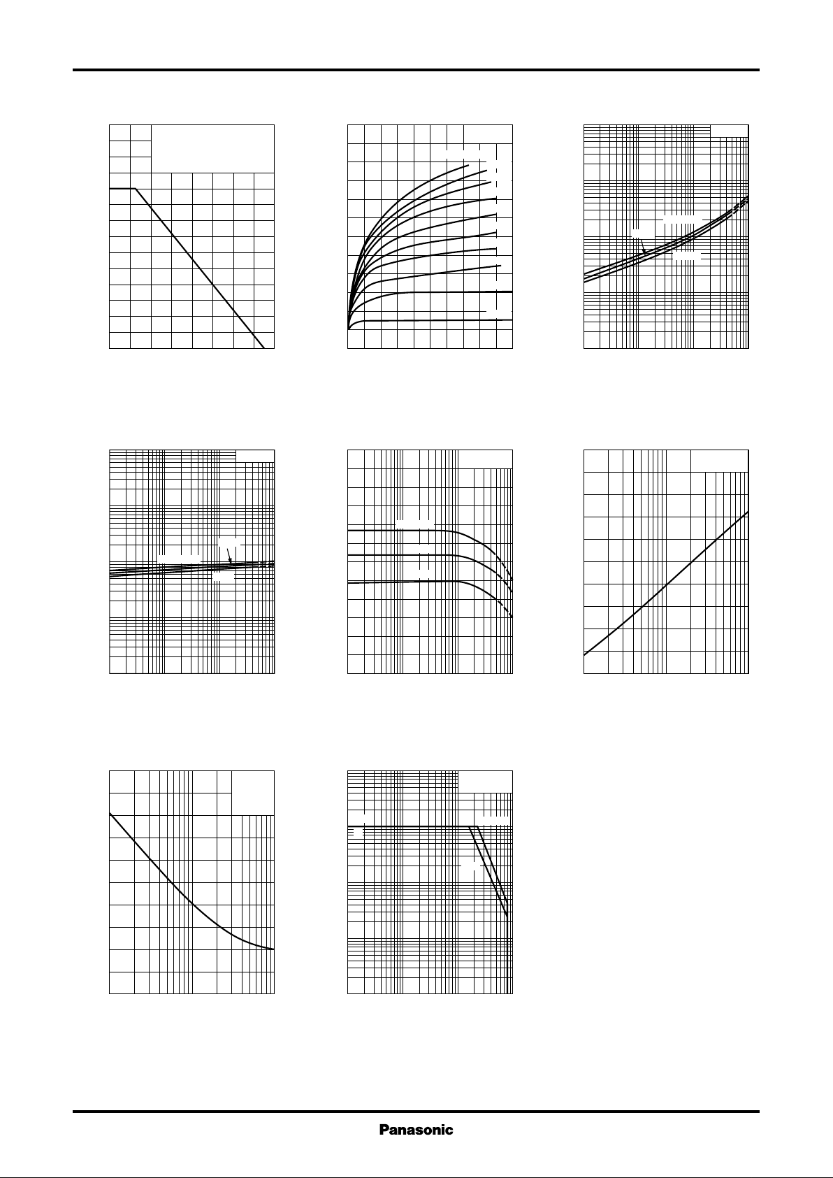
PC — Ta IC — V
1.4
)
W
1.2
(
C
1.0
0.8
0.6
0.4
0.2
Collector power dissipation P
0
0 16040 12080 14020 10060
–100
)
V
(
–30
BE(sat)
–10
–3
–1
– 0.3
– 0.1
– 0.03
Base to emitter saturation voltage V
– 0.01
–1 –10 –100 –1000–3 –30 –300
Printed circut board: Copper
foil area of 1cm
the board thickness of 1.7mm
for the collector portion.
2
or more, and
Ambient temperature Ta (˚C
V
— I
BE(sat)
Ta=–25˚C
C
IC/IB=10
25˚C
75˚C
Collector current IC (mA
V
CE
)
–10
V
(
–3
CE(sat)
–1
– 0.3
– 0.1
– 0.03
– 0.01
– 0.003
– 0.001
Collector to emitter saturation voltage V
–1 –10 –100 –1000–3 –30 –300
Collector current IC (mA
200
180
)
160
MHz
(
140
T
120
100
80
60
40
Transition frequency f
20
0
1 3 10 30 100
Emitter current IE (mA
)
A
(
–1.2
–1.0
– 0.8
C
– 0.6
– 0.4
Ta=25˚C
IB=–10mA
–9mA
–8mA
–7mA
–6mA
–5mA
–4mA
–3mA
–2mA
Collector current I
– 0.2
0
0 –10–8–2 –6–4
)
)
Collector to emitter voltage VCE (V
hFE — I
300
FE
250
200
150
100
50
Forward current transfer ratio h
0
–1 –10 –100 –1000–3 –30 –300
Ta=75˚C
C
25˚C
–25˚C
Collector current IC (mA
–1mA
)
VCE=–10V
)
CE(sat)
25˚C
fT — I
— I
Ta=75˚C
–25˚C
E
C
VCB=–10V
Ta=25˚C
IC/IB=10
)
)
Cob — V
50
)
45
pF
(
40
ob
35
30
25
20
15
10
5
Collector output capacitance C
0
–1 –3 –10 –30 –100
CB
Collector to base voltage VCB (V
2
IE=0
f=1MHz
Ta=25˚C
Area of safe operation (ASO)
–10
–3
I
)
CP
–1
A
(
I
C
C
– 0.3
– 0.1
– 0.03
– 0.01
Collector current I
– 0.003
– 0.001
– 0.1 –1 –10 –100– 0.3 –3 –30
)
Collector to emitter voltage VCE (V
Single pulse
Ta=25˚C
t=10ms
t=1s
)
 Loading...