

Panasonic 2SB0644, 2SB0643 Datasheet
Transistor
2SB643, 2SB644
Silicon PNP epitaxial planer type
For low-power general amplification
Complementary to 2SD638 and 2SD639
Features
■
●
M type package allowing easy automatic and manual insertion as
well as stand-alone fixing to the printed circuit board.
Absolute Maximum Ratings (Ta=25˚C)
■
Parameter
Collector to
base voltage
Collector to
emitter voltage
2SB643
2SB644
2SB643
2SB644
Emitter to base voltage
Peak collector current
Collector current
Collector power dissipation
Junction temperature
Storage temperature
Electrical Characteristics (Ta=25˚C)
■
Parameter
Collector cutoff current
Collector to base
voltage
Collector to emitter
voltage
Emitter to base voltage
Forward current transfer ratio
Collector to emitter saturation voltage
Transition frequency
Collector output capacitance
*1
h
Rank classification
FE1
Rank Q R S
h
FE1
85 ~ 170 120 ~ 240 170 ~ 340
2SB643
2SB644
2SB643
2SB644
Symbol
V
CBO
V
CEO
V
EBO
I
CP
I
C
P
C
T
j
T
stg
Symbol
I
CBO
I
CEO
V
CBO
V
CEO
V
EBO
*1
h
FE1
h
FE2
V
CE(sat)
f
T
C
ob
Ratings
–30
–60
–25
–50
–7
–1
– 0.5
600
150
–55 ~ +150
VCB = –20V, IE = 0
VCE = –20V, IB = 0
IC = –10µA, IE = 0
IC = –2mA, IB = 0
IE = –10µA, IC = 0
VCE = –10V, IC = –150mA
VCE = –10V, IC = –500mA
IC = –300mA, IB = –30mA
VCB = –10V, IE = 10mA, f = 200MHz
VCB = –10V, IE = 0, f = 1MHz
Unit
V
V
V
A
A
mW
˚C
˚C
Conditions
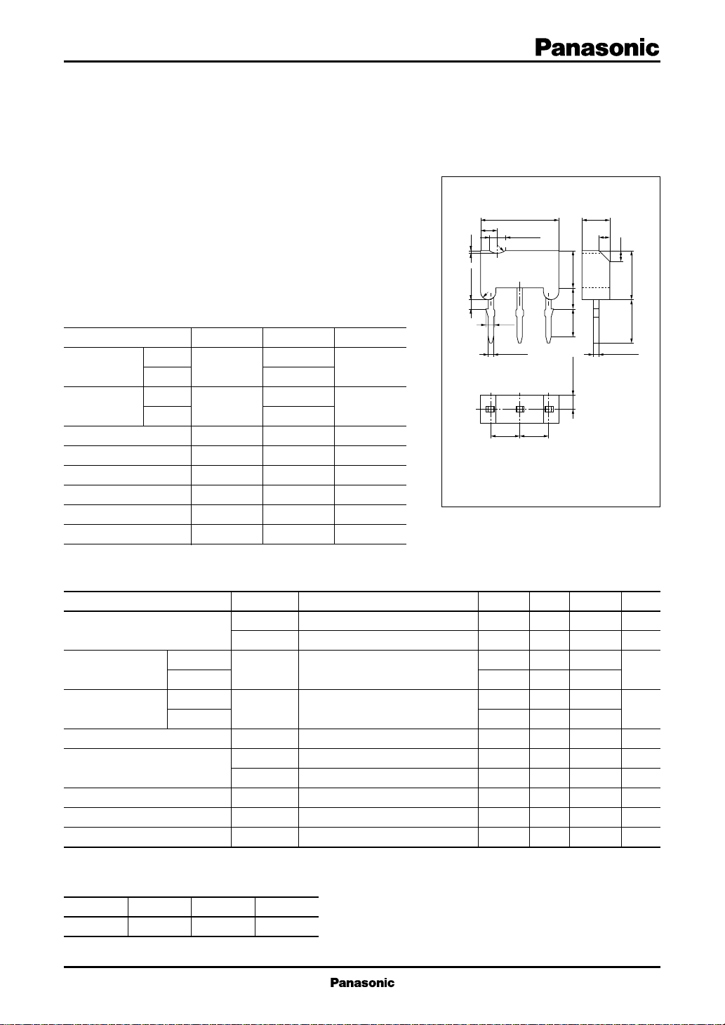
6.9±0.1
1.5
1.5 R0.9
0.4
R0.9
R0.7
1.0±0.1
0.85
0.55±0.1 0.45±0.05
123
2.5 2.5
1:Base
2:Collector EIAJ:SC–71
3:Emitter M Type Mold Package
min
typ
–30
–60
–25
–50
–7
*2
*2
*2
85
40
90
– 0.35
200
6
Unit: mm
2.5±0.1
1.0
1.0
3.5±0.1
2.0±0.2
2.4±0.21.25±0.05
max
4.1±0.2 4.5±0.1
Unit
–100
–1
340
– 0.6
MHz
15
*2
Pulse measurement
nA
µA
V
V
V
V
pF
1
Transistor
2SB643, 2SB644
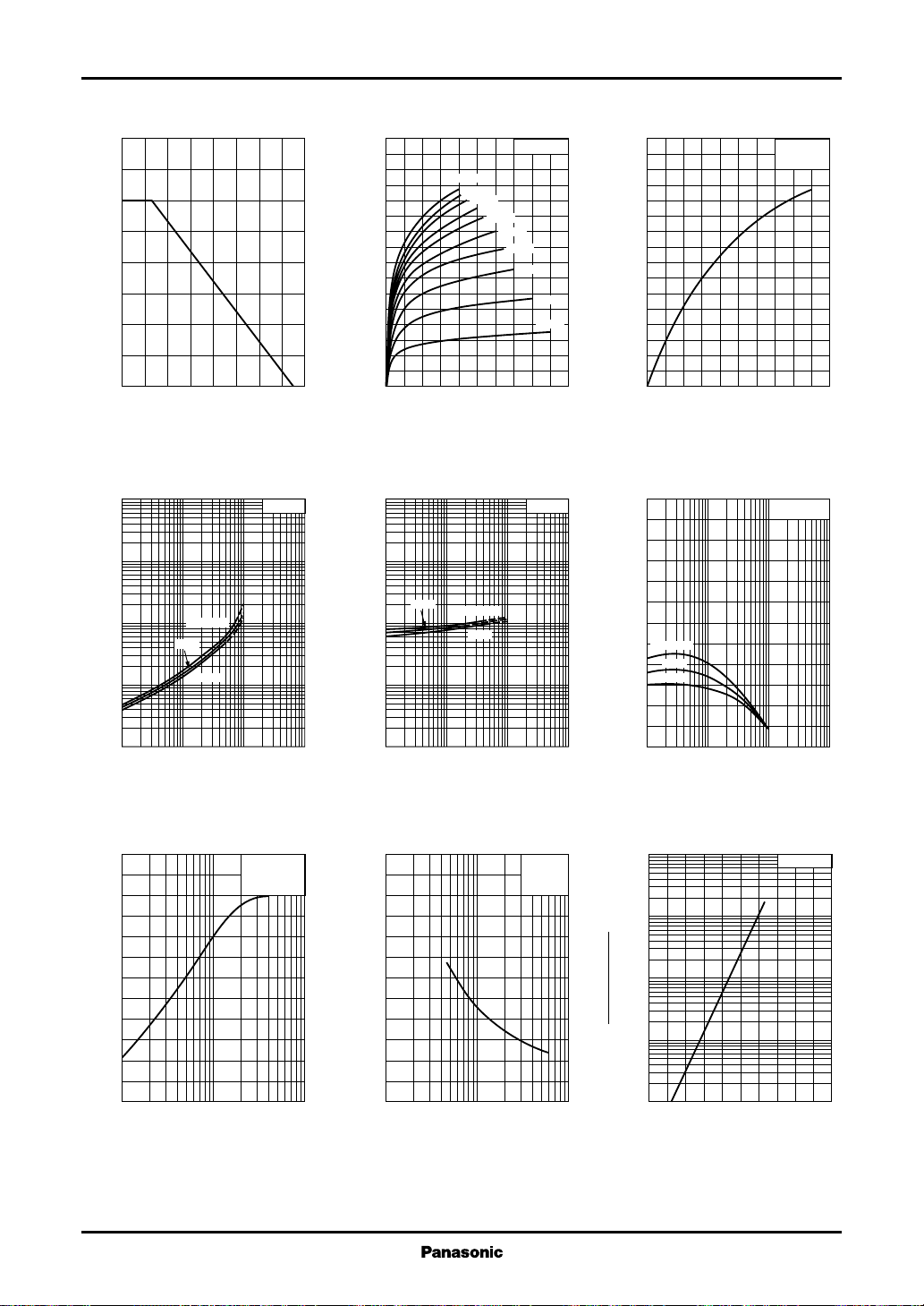
PC — Ta IC — V
800
)
700
mW
(
C
600
500
400
300
200
100
Collector power dissipation P
0
0 16040 12080 14020 10060
Ambient temperature Ta (˚C
V
— I
CE(sat)
)
–100
V
(
–30
CE(sat)
–10
–3
–1
– 0.3
– 0.1
– 0.03
– 0.01
Collector to emitter saturation voltage V
– 0.01
Ta=75˚C
25˚C
–25˚C
– 0.1 –1 –10
– 0.03
– 0.3 –3
Collector current IC (A
)
C
IC/IB=10
)
CE
–800
–700
)
–600
mA
(
C
–500
–400
–300
–200
Collector current I
–100
0
0 –20–16–4 –12–8
IB=–10mA
–9mA
–8mA
–7mA
–6mA
–5mA
Ta=25˚C
–4mA
–3mA
–2mA
–1mA
Collector to emitter voltage VCE (V
V
— I
BE(sat)
–100
)
V
(
–30
BE(sat)
–10
–3
25˚C
–1
– 0.3
– 0.1
– 0.03
Base to emitter saturation voltage V
– 0.01
– 0.01
– 0.1 –1 –10
– 0.03
Collector current IC (A
C
IC/IB=10
Ta=–25˚C
75˚C
– 0.3 –3
)
–800
–700
)
–600
mA
(
C
–500
–400
–300
–200
Collector current I
–100
0
0 –10–8–2 –6–4
)
Base current IB (mA
hFE — I
600
FE
500
400
300
Ta=75˚C
25˚C
200
–25˚C
100
Forward current transfer ratio h
0
– 0.01
–0.1 –1 –10
– 0.03
Collector current IC (A
IC — I
B
– 0.3 –3
C
VCE=–10V
Ta=25˚C
)
VCE=–10V
)
fT — I
240
)
200
MHz
(
T
160
120
80
40
Transition frequency f
0
1 3 10 30 100
Emitter current IE (mA
2
E
VCB=–10V
Ta=25˚C
)
)
pF
(
Cob — V
24
20
ob
16
12
8
4
CB
Collector output capacitance C
0
–1 –3 –10 –30 –100
Collector to base voltage VCB (V
IE=0
f=1MHz
Ta=25˚C
I
— Ta
CEO
4
10
3
10
VCE=–10V
)
)
Ta
(
2
10
Ta=25˚C
(
CEO
I
CEO
I
10
1
0 20016040 12080
)
Ambient temperature Ta (˚C
)
 Loading...