


UG-0011 Jan 05
OX16PCI954
Evaluation Board
Oxford Semiconductor Limited
25 Milton Park
Abingdon
Oxfordshire
OX14 4SH, UK
(44) 1235 824900
User Guide
http://www.oxsemi.com

OX16PCI954 Evaluation Board User Guide
All trademarks are the property of their respective owners
© Oxford Semiconductor Limited 2005
The content of this manual is furnished for informational use only, is subject to change without notice, and should not
be construed as a commitment by Oxford Semiconductor Limited. Oxford Semiconductor Limited assumes no
responsibility or liability for any errors or inaccuracies that may appear in this book.
ii External—Free Release UG-001 1 Jan 05

Contents
Contents . . . . . . . . . . . . . . . . . . . . . . . . . . . . . . . . . . . . . . . . . . . . . . . . . . . . . . . . . . . . . . . iii
Preface . . . . . . . . . . . . . . . . . . . . . . . . . . . . . . . . . . . . . . . . . . . . . . . . . . . . . . . . . . . . . . . . .v
Revision Information . . . . . . . . . . . . . . . . . . . . . . . . . . . . . . . . . . . . . . . . . . . . . . . . . v
Typographic Conventions . . . . . . . . . . . . . . . . . . . . . . . . . . . . . . . . . . . . . . . . . . . . . v
Product Details . . . . . . . . . . . . . . . . . . . . . . . . . . . . . . . . . . . . . . . . . . . . . . . . . . . . .vi
Contacting Oxford Semiconductor . . . . . . . . . . . . . . . . . . . . . . . . . . . . . . . . . . . . . .vi
Chapter 1 Evaluation Board Overview . . . . . . . . . . . . . . . . . . . . . . . . . . . . . . . . . . . . . .1
Features . . . . . . . . . . . . . . . . . . . . . . . . . . . . . . . . . . . . . . . . . . . . . . . . . . . . . . . . . .1
Configuration . . . . . . . . . . . . . . . . . . . . . . . . . . . . . . . . . . . . . . . . . . . . . . . . . . . . . . .2
Drivers . . . . . . . . . . . . . . . . . . . . . . . . . . . . . . . . . . . . . . . . . . . . . . . . . . . . . . . . . . . .2
Board Layout . . . . . . . . . . . . . . . . . . . . . . . . . . . . . . . . . . . . . . . . . . . . . . . . . . . . . . .3
Chapter 2 Evaluation Board Features . . . . . . . . . . . . . . . . . . . . . . . . . . . . . . . . . . . . . .5
Jumpers . . . . . . . . . . . . . . . . . . . . . . . . . . . . . . . . . . . . . . . . . . . . . . . . . . . . . . . . . . .5
Headers & Connectors . . . . . . . . . . . . . . . . . . . . . . . . . . . . . . . . . . . . . . . . . . . . . . . 6
Chapter 3 Configuring the Evaluation Board . . . . . . . . . . . . . . . . . . . . . . . . . . . . . . . . 11
Device Modes . . . . . . . . . . . . . . . . . . . . . . . . . . . . . . . . . . . . . . . . . . . . . . . . . . . . .12
EEPROM Configuration Using OxProm . . . . . . . . . . . . . . . . . . . . . . . . . . . . . . . . .14
Motorola Mode . . . . . . . . . . . . . . . . . . . . . . . . . . . . . . . . . . . . . . . . . . . . . . . . . . . .14
Selecting Clocks . . . . . . . . . . . . . . . . . . . . . . . . . . . . . . . . . . . . . . . . . . . . . . . . . . .15
Drivers . . . . . . . . . . . . . . . . . . . . . . . . . . . . . . . . . . . . . . . . . . . . . . . . . . . . . . . . . . .15
UG-0011 Jan 05 External—Free Release iii

Contents OX16PCI954 Evaluation Board User Guide
Appendix A Drivers . . . . . . . . . . . . . . . . . . . . . . . . . . . . . . . . . . . . . . . . . . . . . . . . . . . . . 17
Driver Process . . . . . . . . . . . . . . . . . . . . . . . . . . . . . . . . . . . . . . . . . . . . . . . . . . . . 17
Using the Serial Driver . . . . . . . . . . . . . . . . . . . . . . . . . . . . . . . . . . . . . . . . . . . . . . 18
Using the Parallel Port Driver . . . . . . . . . . . . . . . . . . . . . . . . . . . . . . . . . . . . . . . . . 20
Appendix B RS422 & RS232 Connector Pin Assignment . . . . . . . . . . . . . . . . . . . . . . 23
RS422 Connector Pins . . . . . . . . . . . . . . . . . . . . . . . . . . . . . . . . . . . . . . . . . . . . . . 23
RS232 Connector Pins . . . . . . . . . . . . . . . . . . . . . . . . . . . . . . . . . . . . . . . . . . . . . . 23
DB9-to-DB25 Converter . . . . . . . . . . . . . . . . . . . . . . . . . . . . . . . . . . . . . . . . . . . . . 24
RS232 Loop-Back Test Plugs . . . . . . . . . . . . . . . . . . . . . . . . . . . . . . . . . . . . . . . . 25
RS232 Null Modem Cables . . . . . . . . . . . . . . . . . . . . . . . . . . . . . . . . . . . . . . . . . . 26
RS232 monitor cable . . . . . . . . . . . . . . . . . . . . . . . . . . . . . . . . . . . . . . . . . . . . . . . 27
Appendix C Customizing the Device Vendor ID & Subsystem ID . . . . . . . . . . . . . . . . 29
Overview . . . . . . . . . . . . . . . . . . . . . . . . . . . . . . . . . . . . . . . . . . . . . . . . . . . . . . . . 29
Examples . . . . . . . . . . . . . . . . . . . . . . . . . . . . . . . . . . . . . . . . . . . . . . . . . . . . . . . . 30
Appendix D Troubleshooting . . . . . . . . . . . . . . . . . . . . . . . . . . . . . . . . . . . . . . . . . . . . . 33
iv External—Free Releas e UG-0011 Jan 05

Preface
The OX16PCI954 evaluation board provides an environment in which
the various modes and features of the OX16PCI954 device can be
demonstrated.
This guide documents the board and explains how to use it to develop
systems using the Oxford Semiconductor OX16PCI954 device. It is
relevant to developers working on implementations using those
products and should be read before using it, to avoid the possibility of
usage errors.
This manual assumes that you understand the capabilities of Oxford
Semiconductor UART products, and are familiar with PCI and PC card
bus interfaces.
Revision
Table I documents the revisions of this manual
Information
Table I Revision Information
Revision Modification
January 2005 First publication in revised house style
Typographic
In this manual, the conventions listed in Table II apply.
Conventions
Table II Typographic Conventions
Convention Meaning
Italic Letters With Initial Capital Letters A cross-reference to another publication
Courier Font Software code, or text typed in via a keyboard
Bold Letters A program, function, class, or method
1, 2, 3 A numbered list where the order of list items is significant
“Title” Cross-refers to another section within the document
UG-0011 Jan 05 External—Free Release v
A list where the order of items is not significant
Significant additional information

Preface OX16PCI954 Evaluation Board User Guide
Product Details
Contacting Oxford Semiconductor
The order code for the OX16PCI954 evaluation board is EV-OX16PCI954.
Oxford Semiconductor contact details:
Oxford Semiconductor Ltd.
25 Milton Park
Abingdon
Oxfordshire
OX14 4SH
United Kingdom
Website: http://www.oxsemi.com
Telephone: +44 (0) 1235 824900
Fax: +44 (0) 1235 821141
Email: sales@oxsemi.com
Alternatively, you can contact your local representative.
vi External—Free Release UG-0011 Jan 05

Chapter 1
Evaluation Board
Overview
The OX16PCI954 evaluation board kit contains the following items:
OX16PCI954 evaluation board (5-V input) with embedded
OX16PCI954 & additional OX16C954 chip
Octopus 8- or 4-way serial cable
Parallel port cable
Additional serial port cable expander
Board documentation, standard configuration files and utility tools such
as OxProm are available from the Oxford Semiconductor website.
Features The evaluation board is an adaptable tool with configurable features
including the following:
4 × OX16C954 UARTs (2xRS232, 2xRS422) accessible via a
standard 37-way D-type interface
8-bit local bus function to drive an external OX16C954 UART
(2×RS232, 2×RS422) from a similar interface
Parallel port function via a standard 25-way D-type header
Serial EEPROM socket for maximum device configurability
Internal crystal oscillator, or any frequency via a TTL oscillator
socket (switchable)—the external OX16C954 can be driven either
from the TTL module or directly from the LB_Clk_Out pin of
the PCI device
Isochronous mode for the internal UARTs via simple connections
Test points so that signals on any bus can be observed easily
UG-0011 Jan 05 External—Free Release 1

Evaluation Board Overview OX16PCI954 Evaluation Board User Guide
Configuration The evaluation board is a valuable tool for assessing the behavior of the
OX16PCI954 device and can be configured to support systems using the
following selectable capabilities:
8-port serial card
4-port serial/1-port parallel card
4-port serial card with pin-assignable subsystem ID & subsystem
vendor ID
32-bit bridge
Chapter 3 Configuring the Evaluation Board explains the board settings
required to operate the OX16PCI954 in these modes.
However, the flexibility of the OX16PCI954 allows users to extend the
capabilities of the chip beyond its primary modes. For example, it is
possible to use the OX16PCI954 in other solutions as follows:
4-port serial/2-port parallel card
2-port serial/1-port parallel card
1-port parallel card
4-port serial/1-port custom FPGA synchronous I/O controller on
the local bus
The correct driver for a specific device mode is selected depending on
the vendor, device and subsystem IDs. For the primary modes of the
OX16PCI954, IDs are pre-allocated and hard-coded; they should not be
changed. However, for customized operational modes, it is necessary to
change the ID fields so that the Windows Plug and Play system can
differentiate boards (even though they use the same chip) and load the
correct driver. Appendix C Customizing the Device Vendor ID &
Subsystem ID outlines recommended procedures for reconfiguring the
hardware drivers to identify custom add-in card configurations.
Drivers The drivers provided for the OX16PCI954 evaluation board have been
written for Windows 2000, Windows NT and Windows XP operating
systems. Although drivers are also available for Linux, they have not
been written by Oxford Semiconductor and Oxford Semiconductor
cannot be held responsible for any aspect of their performance.
2 External—Free Release UG-0011 Jan 05
For further information about device drivers, see “Drivers” on page 11.
OX16PCI954 Evaluation Board User Guide Evaluation Board Overview
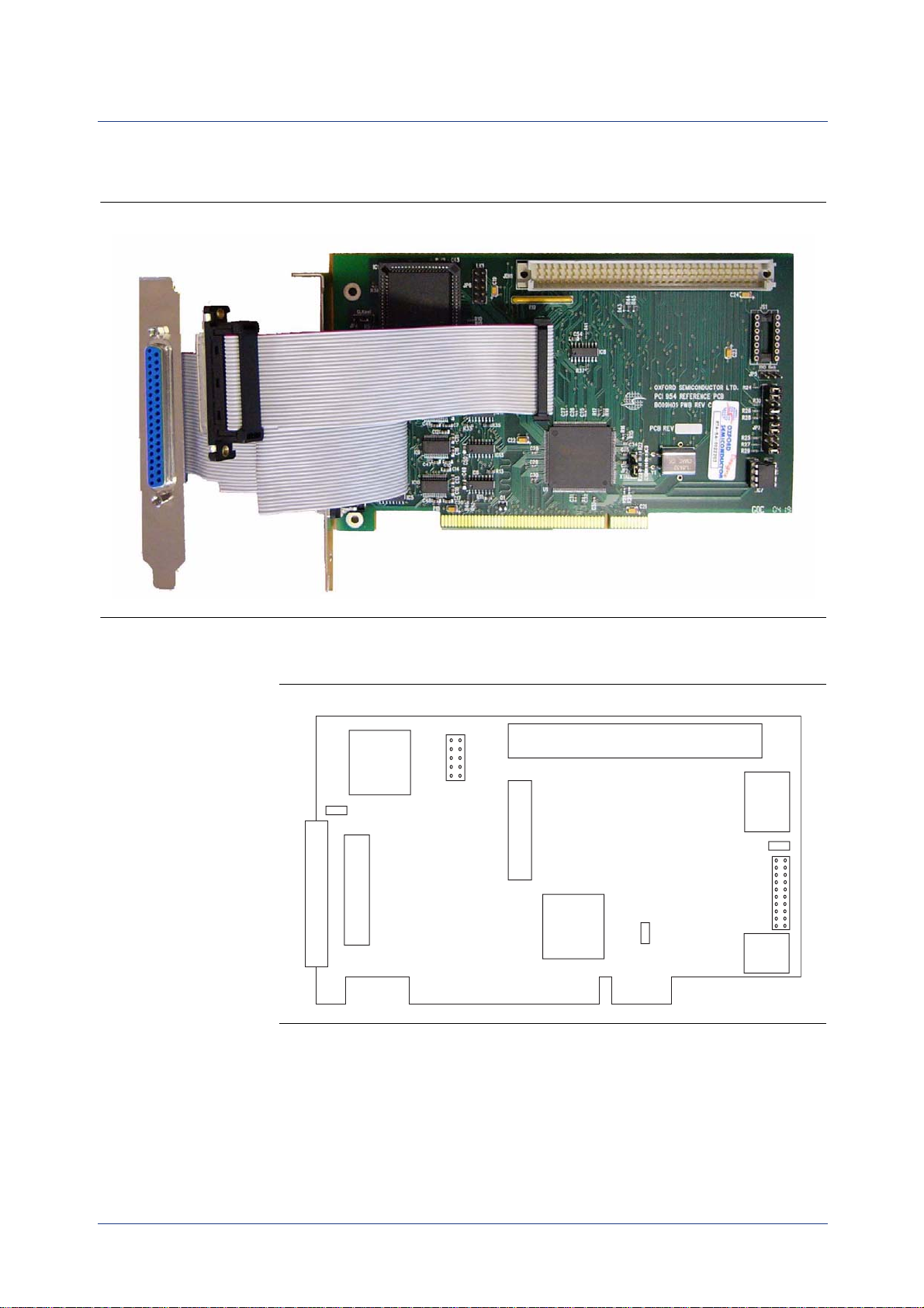
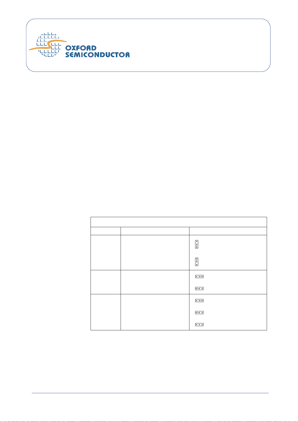
Board Layout Figure 1 on page 3 shows the OX16PCI954 evaluation board.
Figure 1 OX16PCI954 Evaluation Board
Figure 2 identifies the principal features on the device.
Figure 2 OX16PCI954 Evaluation Board Features
IC1 External
OX16C954
JP4 CLKsel
1
Serial Ports
JP1 External OX16C954
P2 OX16PCI954 Serial Ports
1
JP6 LK1
1
1
JP1 Parallel Port
PCI Connector
U1
OX16PCI954
JDH1 Test Pin Header
1
JP2 XTALsel
1
Oscillator
JP5 RIO link
1
EEPROM
JS1
Crystal
Socket
1
JP3
JC7
Serial
For greater detail, a reference schematic for the OX16PCI954 evaluation
board can be requested from Oxford Semiconductor.
Chapter 2 Evaluation Board Features gives further details about the
features of the OX16PCI954 evaluation board.
UG-0011 Jan 05 External—Free Release 3

Evaluation Board Overview OX16PCI954 Evaluation Board User Guide
This page is intentionally blank
4 External—Free Release UG-0011 Jan 05
Chapter 2
Evaluation Board
Features
The OX16PCI954 evaluation board contains a variety of sockets, jumpers,
connectors and headers, which enhance its flexibility.
Jumpers Tabl e 1 details the jumpers on the board and their use.
Table 1 Jumpers on the OX16PCI954 Evaluation Board
Jumper Use Selection
JP2 XTALsel Selects the oscillator type for the
OX16PCI954
JP4 CLKsel Selects the oscillator type for the
external UART
(2)
RIO link
Note:
1 If this is fitted, a TTL crystal oscillator must be connected to JS1.
2 If this is used, MIO0 must be reconfigured in LCC, otherwise an interrupt is constantly present on
function 0
Connects MIO 0 to RI of either
PCI UART channel 0 or external
UART channel 0
Crystal oscillator (as supplied)
TTL oscillator
LB_Clk_out(as supplied)
TTL module
External UART RIO
PCI UART RIO
Open (as supplied)
(1)
UG-0011 Jan 05 External—Free Release 5

Evaluation Board Features OX16PCI954 Evaluation Board User Guide
Headers & Connectors
The OX16PCI954 evaluation board has the following headers and
connectors:
JP3—configuration header
JP6 LK1—DTR/DSR header for RS422 channels
JDH1—test header
P2—37-way D-type connector
JP1—header giving access to the external UART serial ports
JP7—parallel port header
JP3
Figure 3 shows JP3, the 10×2 configuration header on the evaluation
board.
Figure 3 JP3 Configuration Header
1
Quad FIFO Select#
NC
NC
INTEN#
Intel/Motorola Mode#
RS422 Enable
NC
Mode1
Mode 0
PCI FIFOSEL
Table 2 lists the pins on JP3 and explains their use.
Table 2 JP3 Settings
Pin Pair Fitted Open
External FIFOSEL# External UART has 128-byte deep FIFOs (as
supplied)
LPTBUF# Parallel port transceiver disabled (as supplied) Parallel port transceiver enabled
Low Power Enable Allow driver to shut down the RS232 line drivers RS232 line drivers always enabled (as supplied)
INTEN# External UART interrupts enabled (as supplied) External UART interrupt-enables depend on
Intel/Motorola# Mode Motorola-type local bus Intel-type local bus (as supplied)
RS422 Enable Enable RS422 line drivers (as supplied) Disable RS422 line drivers
Test Always short Do not open the connection
Mode1
Mode0
(1)
(1)
Mode[1] = 1 Mode[1] = 0 (as supplied)
Mode[0] = 1 Mode[0] = 0 (as supplied)
PCI FIFOSEL PCI UART has 128-byte deep FIFOs (as supplied) PCI UART has 16-byte deep FIFOs
Note: 1 The combined effect of these pin settings determines the operational mode of the evaluation board; see
Chapter 3 Configuring the Evaluation Board for further details.
External UART has 16-byte deep FIFOs
MCR[3]
6 External—Free Release UG-0011 Jan 05

OX16PCI954 Evaluation Board User Guide Evaluation Board Features
JP6 LK1
Figure 3 shows JP6 LK1, which is the 5×2 DTR/DSR header for RS422
channels on the evaluation board.
The OX16PCI954 evaluation board supports two RS422 ports. Data
transfer rates are much greater using RS422 protocol, because it uses
differential signalling. However, RS422 connectors only allow for CTS/
RTS flow control. JP6 LK1 provides access to the hardware lines
necessary to provide DTR/DSR flow control in addition to conventional
CTS/RTS flow control.
Figure 4 JP6 LK1
1
DSR2DSR2+
GND
DSR3DSR3+
DTR2DTR2+
DTR3DTR3+
NC
RS422 connection via a 9-way D connector is documented in Appendix B
RS422 & RS232 Connector Pin Assignment.
JDH1
Figure 5 shows JDH1, which is the test header on the evaluation board.
All non-PCI pins can be accessed from this header.
Figure 5 JDH1
1 32
A
B
C
Table 3 on page 8 lists the pin allocations on JDH1.
.
UG-0011 Jan 05 External—Free Release 7

Evaluation Board Features OX16PCI954 Evaluation Board User Guide
Table 3 P1 Pin Allocations
Pin
No.
1 MIO 0 MIO 1 MIO 2
2 MIO 3 MIO 4 MIO 5
3 MIO 6 MIO 7 LBRST#
4 PE BUSY ACK#
5 SLCT ERR# LBCS0#
6 LBCS1# LBCS2# LBCS3#
7LBRD# LBWR# GND
8 GND LBCLK GND
9 SLIN# INIT# AFD#
10 STB# GND LBDOUT
11 LBD0 LBD1 LBD2
12 LBD3 GND LBD4
13 LBD5 LBD6 LBD7
14 MIO 8 MIO 9 MIO 10
15 MIO 11 RXD5 RI5
16 DCD5 DSR5 CTS5
17 DTR5 RTS5 GND
18 GND GND GND
19 SOUT5 SOUT4 RTS4
20 DTR4 CTS4 DSR4
21 DCD4 RI4 GND
22 GND UART_Clk GND
23 SIN4 SIN1 RI1
24 DCD1 DSR1 CTS1
25 DTR1 RTS1 SOUT1
26 SOUT0 RTS0 DTR0
27 CTS0 DSR0 DCD0
28 RI0 SIN0 GND
29 GND FIFOSEL VCC
30 GND TEST VCC
31 GND MODE1 VCC
32 GND MODE0 VCC
Row A Row B Row C
P2
On the evaluation board, P2 is a 37-way D-type connector which is used
to access the PCI UART serial ports. Table 4 on page 9 lists the pin
allocations on the connector.
8 External—Free Release UG-0011 Jan 05

OX16PCI954 Evaluation Board User Guide Evaluation Board Features
Table 4 37-Way D-Type Connector Pins
Port Number/
Type
37-Way D-Type
Pin No.
9-Way D-Type
Pin No.
Description
Port 1/RS232 1 1 DCD
20 6 DSR
22RxD
21 7 RTS
33TxD
22 8 CTS
44DTR
23 9 RI
55GND
Port 2/RS232 24 1 DCD
66DSR
25 2 RxD
77RTS
26 3 TxD
88CTS
27 4 DTR
99RI
28 5 GND
Port 3/RS422 10 1 DCD
29 6 DSR
11 2 RxD
30 7 RTS
12 3 TxD
31 8 CTS
13 4 DTR
32 9 RI
14 5 GND
Port 4/RS422 33 1 DCD
15 6 DSR
34 2 RxD
16 7 RTS
35 3 TxD
17 8 CTS
36 4 DTR
18 9 RI
37 5 GND
NC 19 NC NC
UG-0011 Jan 05 External—Free Release 9

Evaluation Board Features OX16PCI954 Evaluation Board User Guide
The pin allocation is also the same for the PCI internal UARTs and the
four ports from the OX16C954 local bus device.
JP1 & JP7
On the evaluation board, JP1 is a header used to access the external
UART serial ports. The pin allocations are the same as for the 37-way D
connector in Tabl e 4. JP7 is used for a parallel port connection.
10 External—Free Release UG-0011 Jan 05

Chapter 3
Configuring the
Evaluation Board
The OX16PCI954 evaluation board can be used to verify a variety of
system designs, because it can be configured to work in different device
modes. The mode depends on the mode pin settings on the board; each
mode enables a specific combination of UART and/or bridge functions.
In addition to the mode pins, other jumpers enable and disable device
features such as clock selection and interrupts, which further refine the
behavior of the evaluation board.
The configuration process determines which driver is used to operate a
configured device, using a system of unique vendor and subsystem IDs
to differentiate modes. The IDs used for the primary device modes
covered in this chapter are hard-coded and should not be changed;
however, the OX16PCI954 is very flexible and can be used for other
solutions which also require unique IDs. Appendix C Customizing the
Device Vendor ID & Subsystem ID outlines recommended procedures
for reconfiguring the hardware drivers to identify custom add-in card
configurations.
This chapter does not cover baud rate configuration for the device. For
further details of how to set the device transfer rate, refer to the
application note OXAN15 Setting Baud Rates Under Windows.
UG-0011 Jan 05 External—Free Release 11

Configuring the Evaluation Board OX16PCI954 Evaluation Board User Guide
Device
Mode pins on the OX16PCI954 evaluation board select the device mode.
The mode pins are located on header JP6 LK1, as shown on Figure 2 on
Modes
page 3.
Selecting the Device Mode
Table 5 shows how the mode pins are used to select the device mode.
Table 5 MODE Pin Settings & Effect
Mode [1] Mode [0] Device Mode
0 0 Quad UARTs (function 0) & 8-bit local bus (function 1)
0 1 Quad UARTs (function 0) & parallel port (function 1)
10
11
Quad UARTs (function 0) & pin-assignable subsystem ID & subsystem vendor ID
32-bit bridge (function 1)
Note:
1 Function 1 is unusable, because the local bus pins ar e us ed f or th e sub system ID & s ubsy stem v endo r ID.
2 Only function 1 is available in this mode.
(2)
Implementing Mode 00—Quad UART/8-Bit Local Bus
(1)
In quad UART/8-bit local bus mode, four internal UARTs are provided
using the OX16PCI954 and four further external UARTs are supplied
using the OX16C954. The key settings for implementing this mode are
listed below:
Mode pins [1:0] must be set to 00
Plug the OX16C954 device into IC1
For the PCI UARTs and the local bus UARTs, channels 0 and 1 interface
via RS232 connections and channels 2 and 3 interface via RS422
connections. The RS422 ports apply flow control using DTR and DSR
signals that are enabled via JP6 LK1. Although it is possible to obtain
basic hardware flow control without DTR and DSR, they are essential for
DTR/DSR flow control or isochronous mode operation. An extra cable is
needed to use DTR/DSR and is implemented as follows:
Connect the extra 37-way D-type connector to JP1
If required, enable the RS422 channels (fit RS422 Enable on
JP6 LK1)
The following jumpers on JP6 LK1 can be fitted as required:
Quad FIFO Select#
INTEN#
Intel/Motorola# Mode
PCI FIFO Select#
12 External—Free Release UG-0011 Jan 05

OX16PCI954 Evaluation Board User Guide Configuring the Evaluation Board
Implementing Mode 01—Quad UART/Parallel Port
In quad UART /parallel port mode, four internal UARTs are provided
using the OX16PCI954 and the parallel port header is used. The key
settings for implementing this mode are listed below:
Mode pins [1:0] must be set to 01
Remove the OX16C954 device from IC1
Connect the parallel port header to P4
For the PCI UARTs, channels 0 and 1 interface via RS232 connections and
channels 2 and 3 interface via RS422 connections. The RS422 ports apply
flow control using DTR and DSR signals that are enabled via JP6 LK1.
Although it is possible to obtain basic hardware flow control without
DTR and DSR, they are essential for DTR/DSR flow control or
isochronous mode operation. An extra cable is needed to use DTR/DSR
and is implemented as follows:
Connect the extra 37-way D-type connector to JP1
If required, enable the RS422 channels (fit RS422 Enable on
JP6 LK1)
The following jumpers on JP6 LK1 can be fitted as required:
External FIFO Select#
INTEN#
Intel/Motorola# Mode
PCI FIFO Select#
If the parallel port is recognized, but will not communicate with the
printer or other device, check that the OX16C954 has been removed from
IC1.
Implementing Mode 10—Quad UART with Assignable IDs
In quad UART with assignable ID mode, four internal UARTs are
provided using the OX16PCI954 and the local bus pins are used to assign
a subsystem ID and subsystem vendor ID. The key settings for
implementing this mode are listed below:
Mode pins [1:0] must be set to 01
Remove the OX16C954 device from IC1
UG-0011 Jan 05 External—Free Release 13

Configuring the Evaluation Board OX16PCI954 Evaluation Board User Guide
For the PCI UARTs, channels 0 and 1 interface via RS232 connections and
channels 2 and 3 interface via RS422 connections. The RS422 ports apply
flow control using DTR and DSR signals that are enabled via JP6 LK1.
Although it is possible to obtain basic hardware flow control without
DTR and DSR, they are essential for DTR/DSR flow control or
isochronous mode operation. An extra cable is needed to use DTR/DSR
and is implemented as follows:
Connect the extra 37-way D-type connector to JP1
If required, enable the RS422 channels (fit RS422 Enable on JP6
LK1)
The following jumpers on JP6 LK1 can be fitted as required:
External FIFO Select#
INTEN#
Intel/Motorola# Mode
PCI FIFO Select#
EEPROM Configuration Using OxProm
Motorola Mode
The OX16PCI954 can be configured via a serial EEPROM if required,
using the Oxford Semiconductor OxProm EEPROM programming
utility. All features of the device can be programmed using OxProm,
which can be downloaded from the Oxford Semiconductor website.
OxProm is bundled with reference drivers, sample configuration files
and supporting documentation including the Oxford Semiconductor
OxProm EEPROM Programming User Guide, which explains how to
program the OX16PCI954 using OxProm.
To configure the OX16PCI954 via its EEPROM, plug the EEPROM into
IC7 on the evaluation board. If the EEPROM has not previously been
programmed, it presents the value 0xFF when OxProm is used to
program it.
The OX16PCI954 local bus can be used in either Intel or Motorola mode,
determined by the Intel/Motorola link setting on JP6 LK1. When the link
is not fitted, the device assumes Intel mode, which is the default setting.
To use the local bus in Motorola mode, fit the Intel/Motorola# Mode link.
With the Motorola mode selection, the default local bus timing values
should be changed in the local control & configuration (LCC) registers as
follows:
Read-not-write de-assertion = 4
Read data-strobe assertion = 1
Write data-strobe assertion = 1
Write data-strobe de-assertion = 3
14 External—Free Release UG-0011 Jan 05

OX16PCI954 Evaluation Board User Guide Configuring the Evaluation Board
Also, MIO [8] in the MIO configuration registers should be configured as
an inverting input, and MIO [9-11] should be masked off. OxProm can be
used to configure these register settings; alternatively, an EEPROM
configuration file containing these settings, motorola.dat, is provided for
this purpose.
Selecting Clocks
An external clock must always be connected to XT1 for the PCI UARTs.
Either an internal crystal oscillator or a TTL oscillator module can be
used; the XTALsel jumper setting specifies the type of oscillator
supplied. See Chapter 2 Evaluation Board Features for more about this
jumper setting.
An additional clock supply is required for the external UARTs on the
OX16C954 device: either the TTL oscillator module (which must be
fitted) or the 0X16PCI954 LB_Clk_Out. The CLKsel link must be fitted
to select the appropriate clock, which must also be enabled or disabled
by writing to the configuration register. The configuration register can
either be updated temporarily using the Microsoft Debug utility, or
permanently by programming the serial EEPROM using OxProm.
Bit 2 of the OX16PCI954 local configuration & control register (LCC)
enables the UART clock output, which is by default low. When this bit is
set, the buffered UART clock output pin, UART_CLK_Out, is active,
otherwise it is permanently low and must be enabled. To enable the
UART clock output, the device must be fitted with an EEPROM and
programmed using OxProm. Specifically, the check box Enable UART
Clock Out in zone 1 must be checked. This means that a single oscillator
can be used to drive serial ports on the local bus as well as the internal
UARTs.
See the Oxford Semiconductor OxProm EEPROM Programming User Guide
for details of how to use OxProm.
Drivers The device operational mode determines which driver is loaded. For
detailed instructions on how to install the reference drivers, see
“Drivers” on page 11.
UG-0011 Jan 05 External—Free Release 15

Configuring the Evaluation Board OX16PCI954 Evaluation Board User Guide
This page is intentionally blank
16 External—Free Release UG-0011 Jan 05

Drivers
Reference drivers and utilities for the Oxford Semiconductor UART
products are supplied to demonstrate functionality under Windows
operating systems. These drivers have been tested using Oxford
Semiconductor development boards in a range of PC systems.
Driver Process
Driver software and any accompanying files are provided ‘as is’ and
without warranties as to performance or merchantability, or any other
warranties whether express or implied.
Windows driver architectures are very similar, utilizing Plug and Play
bus drivers which create device objects for each available UART and
parallel port. New driver installation commences when the configured
device is connected to the PC, although subsequent actions can vary
slightly depending on the operating system. For Windows systems other
than Windows NT4, the driver installation process is as follows:
1 Each UART is hooked by a single-port driver, which enables the
following features:
128-byte receiver & transmitter FIFOs
Adjustable receiver & transmitter interrupt trigger level
Automatic flow control
Quad speed—using the Times clock register (TCR)
Flexible baud rate generation up to 15 Mbaud
RS485 half-duplex configuration
Memory-mapped operation (Windows 2000 driver only)
2. The local bus/parallel port is hooked to the generic driver
supplied with Windows.
UG-0011 Jan 05 External—Free Release 11
The drivers automatically recognize the device in any of its default or
standard configurations.
In Plug and Play systems, a wizard automatically starts up when a new
device is detected, to assist with device management. Although it is
necessary to direct the wizard to the location of the driver files, the
wizard handles device and driver installation automatically.
For more help with device installation, see the Windows Help facility.

Drivers OX16PCI954 Evaluation Board User Guide
Using the Serial Driver
The serial drivers are highly configurable. They make use of a number of
enhanced features for the Oxford Semiconductor 950-series UARTs.
This section describes the configuration utilities that can be used to
enable and configure driver features. It assumes that you are using a
Win 2K or Windows XP operating system. However, Oxford
Semiconductor also provides additional drivers for the OX16PCI954 as
follows:
Drivers for Win 9x and Windows ME, which are similar to
Win 2K and Windows XP drivers
Win NT4 driver, which is a single non-Plug and Play driver with
limited configuration options
For further details about any of these drivers, contact Oxford
Semiconductor.
The driver automatically installs the correct number of serial ports, to
which the Windows operating system assigns COM numbers (e.g.,
COM5). You can then attach modems etc. to the ports and use them in
the same way as any other generic port. However, extra configuration
options are available in addition to the standard settings tab supplied
with generic drivers. Follow the steps below to adjust the UART serial
parameters:
1 Display the Control Panel and select the device manager (if nec-
essary, consult the Windows help facility for details of how to do
this).
2. Ensure that the Devices by type viewing option is selected.
3. Click the + by Ports (COM & LPT) to review the installed PCI
COM ports.
4. Double-click the appropriate Oxford Semiconductor PCI COM
port to display its properties dialog.
Three tags in the dialog are used to configure enhanced device features:
Settings—for standard COM port settings
Data rate—advanced data rate selection options
FIFOs—device mode selection and FIFO trigger level settings
Settings
The Settings tag groups the standard baud rate, data bits, parity, stop bits
and flow control options for standard COM port settings. The settings
modify the defaults used by Windows, although most applications that
use COM ports override the settings with their own parameters.
12 External—Free Release UG-0011 Jan 05
An application’s baud rate is scaled up if a faster crystal is used.

OX16PCI954 Evaluation Board User Guide Drivers
This tag also allows users to select RS232, RS422, or RS485 half-duplex
operation. The following points are worth noting for these options:
For RS232 applications the DTR pin should be configured as
normal
For RS485, the driver can configure the DTR pin as either active-
high or active-low
DTR/DSR flow control is not allowed for RS422/485, because
these pins are not defined in RS422 protocols
Data Rate
The Data Rate dialog is used to set the clock frequency and baud rate.
For normal operation, the serial driver generates the baud rate from the
crystal frequency. The baud rate can optionally be adjusted as required.
Click Detect Crystal Frequency to detect the input clock frequency to the
UART, otherwise select the frequency from the Crystal Frequency
(MHz) drop-down box.
For automatic crystal detection, no other application can be using the
port.
On initial entry to this dialog, the Use default baud rate check box is
checked; unchecking it enables the following options for overriding the
port configuration:
Baud rate multiplier—checking this box allows you to select a
value from the drop-down box to scale up the baud rate
Quad speed—checking this box results in all application-selected
baud rates being multiplied by four, using the OX16C954 TCR
register
Baud rate divider (prescaler)—checking this box allows you to
select a value from the drop-down box to scale down the selected
baud rate
Using the facilities in this dialog box, a high speed crystal can be predivided to generate standard baud rates or scaled up to allow higher
data rates.
FIFOs
The FIFOs dialog is used to configure 950 mode, which operates with full
128-byte FIFOs, fully adjustable trigger levels and thresholds for
generating interrupts and applying automatic flow-control. This dialog
can also disable the FIFOs completely, although it is not recommended
for normal operation.
Clicking the Use FIFO buffers check box enables the four sliders:
UG-0011 Jan 05 External—Free Release 13

Drivers OX16PCI954 Evaluation Board User Guide
FIFO Interrupt Transmitter levels
Transmitter—a transmitter interrupt is triggered when
the level of data in the transmit FIFO falls below this
value. Setting the trigger to zero suppresses interrupts
until the transmitter is completely idle
Receiver—a receiver data interrupt is triggered when the
level of data in the receiver FIFO reaches this value.
Receiver FIFO Flow Control Thresholds
Flow On—the FIFO fill level decreases as data is read
from the FIFO, until it reaches this value, which triggers a
handshake to instruct the remote transmitter to transmit
data (i.e., it transmits an XON character to the remote
machine)
Flow Off—the FIFO fill level increases as data is put into
the FIFO, until it reaches this value, which triggers a
handshake to instruct the remote transmitter to stop
transmitting data (i.e., it transmits an XOFF character to
the remote machine)
Using the Parallel Port Driver
The FIFO trigger levels and thresholds can be fine-tuned for optimum
performance.
In some cases, a high receiver FIFO interrupt trigger level can result in
the port not detecting Plug and Play serial devices.
This section describes the configuration utilities that can be used to
enable and disable the parallel port.
Win 2K & Windows XP Parallel Port Configuration
Interrupts from the parallel port can be enabled and disabled using the
Windows Device Manager. To adjust the setting, follow these steps:
1 Display the Control Panel and select the Device Manager (if nec-
essary, consult the Windows help facility for details of how to do
this).
2. Ensure that the Devices by type viewing option is selected.
3. Click the + by Ports (COM & LPT) to review the installed PCI
COM ports.
4. Double-click the appropriate Oxford Semiconductor PCI Parallel
port to display the settings dialog for that port
5. Click the Port Settings tab and enable or disable the interrupt as
required
14 External—Free Release UG-0011 Jan 05

OX16PCI954 Evaluation Board User Guide Drivers
Win 9x & Windows ME Parallel Port Configuration
The parallel port driver sets the hardware to use legacy addresses 378h if
available, otherwise it uses the address allocated by the system BIOS.
Windows allocates an LPT number (e.g. LPT2) to the port; then it can be
used in the same fashion as any generic parallel port.
Due to a contention with ISAPNP bus enumeration, some systems do not
work if a port uses 278h or 678h, while some peripheral devices such as
zip drives do not operate correctly if the parallel port is not located at
address 278h or 378h. It might be necessary to experiment and move
conflicting devices to another address.
UG-0011 Jan 05 External—Free Release 15

Drivers OX16PCI954 Evaluation Board User Guide
This page is intentionally blank
16 External—Free Release UG-0011 Jan 05

RS422 & RS232 Connector
Pin Assignment
This appendix discusses the use of RS422 and RS232 9-pin and 25-pin
connectors in systems using the device evaluation board.
RS422 Connector Pins
RS232 Connector Pins
Figure 4 shows how RS422 ports are connected on 9-way D-connectors.
Figure 4 RS422 Pin Assignments
1
6
2
7
3
8
4
9
5
TXD–
RXD–
TXD+
RXD+
RTS–
CTS–
RTS+
CTS+
GND
Data transfer rates are much greater using RS422 protocol, because it
uses differential signalling. However, RS422 connectors only allow for
CTS/RTS flow control.
Although the RS232 interface is differential (the receive and transmit
pins each have their own floating ground level), it is possible to connect
RS232-compatible devices with this interface.
The convention for the RS232 diagrams below is to show signals
common to both connector types in black. Signals only present on the
larger connector are shown in grey.
The protective ground is assigned to a pin at the large connector where
the connector outside is used for that purpose in the DB9 connector.
Figure 5 on page 18 shows the RS232 DB9 pin assignment.
UG-0011 Jan 05 External—Free Release 17

RS422 & RS232 Connector Pin Assignment OX16PCI954 Evaluation Board User Guide
r
Figure 5 RS232 DB 9 Pin-Assignment
1
6
2
7
3
8
4
9
5
Data Carrier Detect
Data Set ready
Receive Data
Request-to-Send
Transmit Data
Clear-to-Send
Data Terminator Ready
Ring Indicator
Signal Ground
Protective Ground
Figure 6 shows the RS232 DB 25-pin assignment.
Figure 6 RS232 DB 25-Pin Assignment
1
14
2
15
3
16
4
17
5
18
6
19
7
20
8
21
9
22
10
23
11
24
12
25
13
Protective Ground
Transmit Data (2)
Transmit Data
Transmitter Clock (DCE)
Receive Data
Receive Data (2)
Request-to-Send
Receiver Clock
Clear-to-Send
Data Set Ready
Request-to-Send (2)
Signal Ground
Data Terminator Ready
Data Carrier Detect
Signal Quality Detector
Test Pin
Ring Indicator
Test Pin
Data Signal Rate Detecto
Transmitter Clock (DTE)
Data Carrier Detect (2)
Clear-to-Send (2)
DB9-to-DB25
The original pin layout for RS232 was developed for a 25-pin
sub D connector, although 9-pin connectors are commonly used. In
Converter
mixed applications, a 9-to-25 pin converter can be used to connect
connectors of different sizes, as shown in Figure 7.
18 External—Free Release UG-0011 Jan 05

OX16PCI954 Evaluation Board User Guide RS422 & RS232 Connector Pin Assignment
Figure 7 RS232 DB9-to-DB25 Converter
RS232 Loop-Back Test Plugs
1
6
2
7
3
8
4
9
5
1
14
2
15
3
16
4
17
5
18
6
19
7
20
8
21
9
22
10
23
11
24
12
25
13
The following connectors can be used to test a PC serial port. The data
and handshake lines are linked so that all data is sent back immediately.
The PC controls its own handshaking.
Figure 8 shows a loop-back that can be used to verify the serial port with
standard terminal software.
Figure 8 RS232 Loop-Back Test Plug for Terminal Emulation Software
1
6
2
7
3
8
4
9
5
1
14
2
15
3
16
4
17
5
18
6
19
7
20
8
21
9
22
10
23
11
24
12
25
13
Figure 9 on page 20 can be used to test the full functionality of the serial
port with Norton Diagnostics or CheckIt.
UG-0011 Jan 05 External—Free Release 19

RS422 & RS232 Connector Pin Assignment OX16PCI954 Evaluation Board User Guide
Figure 9 RS232 Loop-Back Test Plug for Norton Diagnostics & CheckIt
RS232 Null Modem Cables
1
6
2
7
3
8
4
9
5
1
14
2
15
3
16
4
17
5
18
6
19
7
20
8
21
9
22
10
23
11
24
12
25
13
The easiest way of connecting two PCs is via a null modem cable,
although the situation is complicated by the variety of null-modem
cables available. For simple connections, a three-line cable connecting the
signal ground, receive and transmit lines is sufficient, as shown in
Figure 10; although some handshaking mechanism might still be
necessary.
Figure 10 Null Modem Cable Without Handshaking
1
6
2
7
3
8
4
9
5
5
9
4
8
3
7
2
6
1
Handshaking mechanisms in null modem cables can be defined in
various ways, such as loop-back handshaking to each PC or complete
handshaking between the two systems. The most common cable types
are shown in Figures 11 to 13.
For a direct cable connection, a null modem cable with loop-back
handshaking is usually acceptable, as shown in Figure 11 on page 21.
20 External—Free Release UG-0011 Jan 05

OX16PCI954 Evaluation Board User Guide RS422 & RS232 Connector Pin Assignment
Figure 11 Null Modem with Loop-Back Handshaking
1
6
2
7
3
8
4
9
5
Figure 12 Null Modem with Partial Handshaking
1
6
2
7
3
8
4
9
5
Figure 13 Null Modem with Full Handshaking
1
6
2
7
3
8
4
9
5
5
9
4
8
3
7
2
6
1
5
9
4
8
3
7
2
6
1
5
9
4
8
3
7
2
6
1
RS232 monitor cable
Figure 14 shows an RS232 cable that can be used to monitor the serial
communication between two devices using a PC. Two sockets are
connected straight through and the PC is connected to the third socket.
Figure 14 RS232 Monitor Cable
1
6
2
7
3
8
4
9
5
D1
1N4148
R1
2.2 K
1
6
2
7
3
8
4
9
5
5
9
4
8
3
7
2
6
1
UG-0011 Jan 05 External—Free Release 21

RS422 & RS232 Connector Pin Assignment OX16PCI954 Evaluation Board User Guide
The monitor cable taps communication from both sides, which means
that the monitored information is garbage if the two devices happen to
communicate simultaneously. However, because most communication
software works in half-duplex mode, this problem does not arise.
22 External—Free Release UG-0011 Jan 05

Customizing the Device
Vendor ID & Subsystem ID
This appendix outlines recommended procedures for reconfiguring the
hardware drivers to identify custom add-in card configurations.
Overview The default vendor ID and device ID are usually acceptable for most
serial and parallel port applications. However, designers using a device
for another purpose must change the following identification fields in
the PCI configuration space:
Vendor I D
Device ID
Subsystem Vendor ID
Subsystem ID
By doing this, Plug and Play systems can differentiate between boards
even when they use the same chip, and load the correct drivers.
Three approaches can be used to identify an add-in card uniquely. They
are all satisfactory, but are listed below in order of preference.
1 Obtain a vendor ID from the PCI special interest group (PCISIG)
& use OxProm to reprogram the vendor ID & subsystem vendor
ID fields with the new value; then choose a device ID &
subsystem ID.
2. Leave the vendor ID & device ID as the Oxford Semiconductor
default values. Obtain a subsystem vendor ID from the PCISIG &
use OxProm to reprogram the subsystem vendor ID fields with
the new value; then choose the subsystem ID.
Older versions of Windows (e.g., Windows 95 or Win NT) do not
support this facility.
3. Use the Oxford Semiconductor identification fields: Oxford
Semiconductor assigns a subsystem ID to the board vendor, who
programs the new value in using OxProm. To request a
subsystem ID value, contact Oxford Semiconductor with a full
functional description of the new add-in card.
UG-0011 Jan 05 External—Free Release 23

Customizing the Device Vendor ID & Subsystem ID OX16PCI954 Evaluation Board User Guide
The first solution is best for Windows NT systems because they do not
recognize subsystem ID values. Windows 2000 systems can identify
different cards if oxpci.inf specifies the subsystem ID values in the
following format:
PCI\VEN_1415&DEV_9501&SUBSYS_00011415
Board vendors should not assign a new device ID or subsystem ID
unless they have obtained their own vendor ID from the PCISIG. Oxford
Semiconductor reserves the right to refuse to allocate a subsystem ID to a
board vendor.
Examples The following examples are provided for illustration only. They
demonstrate methods of modifying the device vendor ID and subsystem
ID fields.
Four Serial, Two Parallel Port Card
For this configuration it is necessary to use the internal UARTs and have
two external parallel port chips on the local bus. The default ID can be
used for the serial ports, but there must be a different ID for the local bus.
The vendor can contact Oxford Semiconductor for a subsystem ID for the
local bus, or obtain a vendor ID and define drivers for the entire card.
The three possible approaches are given in Table s 6 to 8.
Table 4 Option 1: Use the Board Vendor's Own PCI Vendor ID
Four Serial Ports (Internal UARTs) Function 0 T wo Parallel Ports (Local Bus) Function 1
Vendor ID
Device ID Chosen by vendor Chosen by vendor
Subsystem Vendor ID
Subsystem ID Chosen by vendor Chosen by vendor
Note: 1 In this example, the vendor ID is assumed to be 0x1234
(1)
0x1234 0x1234
(1)
0x1234 0x1234
In this case, the devices must be identified in oxpci.inf as follows:
PCI\VEN_1234&DEV_XXXX
PCI\VEN_1234&DEV_YYYY
where XXXX and YYYY are appropriate device ID for the UART.
Table 5 Option 2: Use the Board Vendor's Own PCI Vendor ID as the Subsystem Vendor ID
Four Serial Ports (Internal UARTs) Function 0 Two Parallel Ports (Local Bus) Function 1
Vendor ID 0x1415 (default) 0x1415 (default)
Device ID 0x9501 (default) 0x9511 (default)
(1)
Subsystem Vendor ID
Subsystem ID Chosen by vendor Chosen by vendor
Note: 1 In this example, the subsystem vendor ID is assumed to be 0x1234
24 External—Free Release UG-0011 Jan 05
0x1234 0x1234

OX16PCI954 Evaluation Board User Guide Customizing the Device Vendor ID & Subsystem ID
In this case, the devices must be identified in oxpci.inf as follows:
PCI\VEN_1415&DEV_9501&SUBSYS_XXXX1234
PCI\VEN_1415&DEV_9511&SUBSYS_YYYY1234
where XXXX and YYYY are appropriate device ID for the UART.
Table 6 Option 3: Obtain a Subsystem ID from Oxford Semiconductor & Use Other Values as Default
Four serial ports (internal UARTs) Function 0 Two parallel ports (Local bus) Function 1
Vendor ID 0x1415 (default) 0x1415 (default)
Device ID 0x9501 (default) 0x9511 (default)
Subsystem Vendor ID 0x1415 (default) 0x1415 (default)
Subsystem ID 0x0001 (default)
Note: 1 In this example, the allocated subsystem ID is assumed to be 0x00FF
0x00FF
(1)
In this case, the devices must be identified in oxpci.inf as follows:
PCI\VEN_1415&DEV_9501&SUBSYS_00011415
PCI\VEN_1415&DEV_9511&SUBSYS_00FF1415
Two Serial, One Parallel Port Card
It is not possible to limit the hardware to enable only two serial ports, so
this solution requires a driver in the enumerator driver, which ensures
that it only registers two ports. Oxford Semiconductor reserves device ID
0x950A for this, so the recommended solution is as shown in Table 4 .
Table 7 Two Serial, One Parallel Port Card
Two Serial Ports (Internal UARTs) Function 0 One Parallel Port (Local Bus) Function 1
Vendor ID 0x1415 0x1415
Device ID 0x950A 0x9513
Subsystem Vendor ID 0x1415 0x1415
Subsystem ID Default Default
Driver versions 2.51 and greater associate device identity 0x950A as a
two-serial port device. Designers should use the first two ports, because
they are the ones that will be used by the driver.
For Windows NT4 systems, oxser.inf must be modified: all occurrences
of 9501 must be changed to 950A before any drivers are installed.
UG-0011 Jan 05 External—Free Release 25

Customizing the Device Vendor ID & Subsystem ID OX16PCI954 Evaluation Board User Guide
One Parallel Port Only
It is not possible to disable the UARTs on the device, so this solution
requires the user to install a null driver for them. Oxford Semiconductor
has assigned a device ID for this (value 0x9500), so the recommended
solution is as shown in Tabl e 5 on page 25.
Table 8 One Parallel Port Only
NULL Function, Function 0 One Parallel Port (Local Bus) Function 1
Vendor ID 0x1415 0x1415
Device ID 0x9500 0x9513
Subsystem Vendor ID 0x1415 0x1415
Subsystem ID Default Default
Drivers recognize device ID 0x9500 as a null function and load a null
driver for this device.
This page is intentionally blank
26 External—Free Release UG-0011 Jan 05

Tables 1 1 to 13 summarize typical difficulties and suggests ways of
overcoming them.
Table 11 Communication Issues (Sheet 1 of 2)
Problem Response
Troubleshooting
Although the system detects the
ports, a terminal application
does not
Some or all ports do not
communicate with other devices
No response running a loop
back test with a terminal
program
The parallel port is recognized,
but does not communicate with
the printer or other device
Ensure that the application supports COM ports other than the four legacy addresses
(3f8, 2f8, 3e8, 2e8). If not, use an application that supports all COM devices, such as
Quarterdeck Procomm Plus, or Ericom PowerTerm
1 Ensure that the baud rates are correct. The 950 series UARTs have a flexible baud
rate generator, which can accept differing crystal frequencies, pre-scaler values etc.
The serial port configuration utility in the driver can set baud rate multipliers or override
an application’s baud rate setting
2 Two of the ports on each UAR T chip have RS422 line drivers on the evaluation board.
These support higher data transfer rates, but do not interface to RS232 ports. Ensure
that the correct ports are in use
3 Ensure that the parallel port transceiver is disabled (close LPTBUF# on JP6 LK1)
4 Ensure that the port has a clock signal, either from the OX16PCI954 oscillator , or from
the TTL clock module. This is selected with XTALsel (internal UARTs) and CLKsel
(local bus UARTs)
1 Ports 1 and 2 are RS232 and ports 3 and 4 are RS422—ensure that the loop back
set-up is correct
2 Check that the loop back connector is wired correctly
1 Ensure that the parallel port transceiver is enabled if present (clear LPTBUF# on
JP6 LK1 on the evaluation board), also remove the OX16CI954 from the PLCC socket
on the evaluation board
2 Ensure that the device is not ECP—the OXPCI954 only supports SPP and EPP
drivers
The local bus does not work in
Motorola mode
When the board is installed in a
system, it complains of a
resource clash
Errors are detected at baud
rates of 300 baud and less
UG-0011 Jan 05 External—Free Release 33
A connector is missing on early development boards. Call Oxford Semiconductor for
details
PCI devices should be able to share interrupts, but some device drivers cannot handle
this feature. If another device is using one of the interrupts assigned to the OX16PCI954,
try one of the following:
1 Move the OX16PCI954 board to a different PCI slot
2 Change the system BIOS settings to allocate different resources (not all BIOS's have
this feature)
3 Use the serial EEPROM to allocate one interrupt to both OX16PCI954 functions
4 Disable any non-critical device using the same interrupt—USB controllers sometimes
cannot share resources adequately
The transmit FIFO length and receive FIFO length are set by default. For lower baud
rates, the difference in length between the transmit and receive FIFOs should not exceed
123

Troubleshooting OX16PCI954 Evaluation Board User Guide
Table 11 Communication Issues (Sheet 2 of 2)
Problem Response
How do I support flow control? To support flow control, set MCR(1) and ECR(7:6)—the hardware then takes care of it. In
addition, if you set IER(7:6) the device asserts a level 6 whenever CTS and RTS toggle
Table 12 Driver Issues (Sheet 1 of 3)
Problem Response
If the EEPROM is programmed
with an invalid image it may not
load the driver; flag an error
To make the OS accept the card, try the following:
1 Unplug the board from the system.
2 Locate the EEPROM on the card & unsolder pin 4 [DO] (This will not allow the
EEPROM to be interrogated by the OS as the data out line is effectively disconnected)
3 Plug the board back in. The system now picks the default settings in the driver which
will not be overwritten by the contents of the EEPROM.
4 Use OXPROM to erase the EEPROM
5 Unplug the board from the system
6 Re-solder pin 4 [DO]
When the system has recognized the card and installed all the appropriate driver files the
board can be used. The EEPROM can then be reprogrammed using one of the .dat files
provided for the OX16PCI954
34 External—Free Release UG-0011 Jan 05

OX16PCI954 Evaluation Board User Guide Troubleshooting
Table 12 Driver Issues (Sheet 2 of 3)
Problem Response
After downloading the drivers,
Device not found appears on
the event viewer
This can happen if either the vendor ID or subsystem ID is changed using OXPROM,
which changes the contents of the EEPROM. The device driver looks for these fields and
does not work if they have been changed. T o change these fields, you have to change the
.inf file.
This can come about due to changes in some of the CIS information in the EEPROM
making it different from information found in the Oxpci.inf file and if a parallel port is being
used Oxpar.inf. For example the line below shows a vendor id of 1415 and no subsystem
id being used.
[ControlFlags]
ExcludeFromSelect=PCI\VEN_1415&DEV_9501
ExcludeFromSelect=PCI\VEN_1415&DEV_9511
ExcludeFromSelect=PCI\VEN_1415&DEV_9521
ExcludeFromSelect=PCI\VEN_1415&DEV_950A
ExcludeFromSelect=PCI\VEN_1415&DEV_950B
ExcludeFromSelect=PCI\VEN_1415&DEV_8401
ExcludeFromSelect=PCI\VEN_1415&DEV_9512
ExcludeFromSelect=PCI\VEN_1415&DEV_9510
ExcludeFromSelect=PCMCIA\PC_CARD-GENERIC-1748
; Drivers
;--------------------------------------------------
[Manufacturer]
%mfg%=mfg
; List of available devices
[mfg]
%PCI\VEN_1415&DEV_9501.DeviceDesc% = PCI_9501,
PCI\VEN_1415&DEV_9501
%PCI\VEN_1415&DEV_9511.DeviceDesc% = PCI_9511,
PCI\VEN_1415&DEV_9511
%PCI\VEN_1415&DEV_950A.DeviceDesc% = PCI_950A,
PCI\VEN_1415&DEV_950A
%PCI\VEN_1415&DEV_950B.DeviceDesc% = PCI_950B,
PCI\VEN_1415&DEV_950B
%PCI\VEN_1415&DEV_8401.DeviceDesc% = PCI_8401,
PCI\VEN_1415&DEV_8401
%PCI\VEN_1415&DEV_9521.DeviceDesc% = PCI_9521,
PCI\VEN_1415&DEV_9521
%PCI\VEN_1415&DEV_9512.DeviceDesc% = PCI_NULL,
PCI\VEN_1415&DEV_9512
%PCI\VEN_1415&DEV_9500.DeviceDesc% = PCI_NULL,
PCI\VEN_1415&DEV_9500
%PCI\VEN_1415&DEV_9510.DeviceDesc% = PCI_NULL,
PCI\VEN_1415&DEV_9510
%Card0.DeviceDesc% = CF_950, PCMCIA\PC_CARD-GENERIC-1748
If changes are made to the vendor and subsystem id then these will have to be changed
in the appropriate .inf files for a driver to be loaded.
Oxprom.exe and 15M operation
does not work in NT
UG-0011 Jan 05 External—Free Release 35
The Oxford Semiconductor NT driver does not support 15M. OxProm does not work in NT .
Source code is available, subject to NDA

Troubleshooting OX16PCI954 Evaluation Board User Guide
Table 12 Driver Issues (Sheet 3 of 3)
Problem Response
Error message The clock for
COM9 was not detected, default
Systems that use 16-bit DLLs cannot auto-detect clock speeds for COM ports >8. It is
necessary to select the device speed manually in Device Manager under Data Rates
to 1843200 Hz appears
Do the drivers support 4 x PCI
Yes
cards?
Ports are not installed correctly
in Windows 2000
1 Check that the driver binaries are present in winnt\system32\drivers
2 Check one of the settings, FIFO or data rate tabs - if it can see the UART it should
identify the device in the top right
3 If the development board is not being used, the UARTs may have mapped to different
memory addresses. Recompile oxmfuf.sys to use I/O mapping—it will be a bit slower
but does not have to work out the memory base address
Table 13 Hardware Issues (Sheet 1 of 2)
Problem Response
I want to use the device from 4.4
to 5.5 volts. What are the
characteristics of the device
over this temp range?
For the supply voltage there is an approximate scaling factor although this is not linear.
The data sheet is specified for the worst case (i.e. 4.75 volts).
Kv (5.00 V) = 1.0
Kv (4.75 V) = 1.04
Kv (4.5 V) = 1.07
where Kv equates to degrees Kelvin.
The process is specified from 4.5 to 5.5 volts.
At 4.4 volts the scaling factor is about 1.1 so the worst case delays are around (1.1/1.04) ×
the original delay
How do I reduce the quiescent
current during standby?
PC will not turn off with the
OX16PCI954 installed
System doesn’t detect the
correct devices
I cannot set the RS485 driver
enables using DTR
At high baud rates the data
throughput is very slow
Which mode allows us to use
MIO pins for our own use?
I am not getting the correct
number in the RFL register
To reduce the quiescent current, tie all pins as internal pull ups and downs as given in the
data sheet. Oscillator leakage figures are not available, but this should be tied to a rail and
not left floating
Apply a PME# pin isolator. Newer demonstration boards have this modification applied
Close TEST link on JP6 LK1 and ensure that the MODE links are set correctly on the
evaluation board. The test pin must be connected to GND
The MCR and ACR registers are required to enable RS485. Set ACR first and then MCR.
Then the chip automatically asserts DTR to transmit
1 The application requests a port at a certain speed. The driver calculates which divider
to use based on criteria including the crystal speed. If the port speed cannot be
achieved within 2%, then it goes slowly. The crystal must be a multiple of 1.8432 MHz
2 First revision evaluation boards have transistors Q1, 2, 3, & 4 just above the PCI
connector. Later versions have resistors in these places
Mode 00 or 01
Read this register until 2 consecutive values are the same. The value can change while it
is being read, and so will output garbage
36 External—Free Release UG-0011 Jan 05

OX16PCI954 Evaluation Board User Guide Troubleshooting
Table 13 Hardware Issues (Sheet 2 of 2)
Problem Response
Which pull-up values are
2k2, as there are no internal pull ups
recommend for STB#, AFD#,
INIT# and SLIN#?
What does mode 10 do? In mode 10 each has 16 pins corresponding to it which allows you to set these values in
hardware. Mode 10 provides a quad-speed UART, but instead of the parallel port or local
bus it has the facility to set Subsystem ID and Vendor ID. This mode allows manufacturers
who do not require the parallel port or local bus to set the Subsystem ID and subsystem
vendor ID without an EEPROM
Why use the 220-k Ω, 470 Ω,
68 pf, 22 pf configuration for the
crystal oscillator?
The feedback resistor is used to add stability because it is being used for a wider range of
frequencies than specified.
Crystal Oscillator Circuit
The OX16PCI954 provides the XTLO output pin to drive a crystal oscillator circuit. The
circuit is shown below with suggested component values. Owing to the nature of such
circuits, some variation in values may be required to ensure stable oscillation at different
frequencies. The total load capacitance (C1 and C2 in series) however, should be
approximately that stated by the crystal manufacturer (nominally 16pF).
XTLO
XTLI
Frequency Range (MHz) C
R
2
R
1
(pF) C2 (pF) R1 (Ω)R
1
C
1
C
2
(Ω)
2
1.8432 - 8 68 22 220k 470R
8-60 33-68 33 – 68 220k-2M2 470R
Note: For better stability use a smaller value of R
. Increase R1 to reduce power
1
consumption.
The total capacitive load (C1 in series with C2) should be that specified by the crystal
manufacturer (nominally 16pF).
If particular problems are encountered with baud rates and the use of drivers options see
the application note Setting UART baud rates under Windows
Does the device support D3
The device does not support D3 cold
cold?
List specifications that the
device complies with?
PCI interface complies with version 2.2 of the PCI Bus Specification and version 1.0 of
PCI Power Management Specification
INTB does not work correctly? 1 Ensure all unused MIO pins are pulled low, otherwise they could generate interrupts.
Also ensure that MIO pins used as inputs do not have a static input (i.e., are pulled
constantly high) as this causes a continuous interrupt to be generated
2 If a static input is required, an EEPROM should be used (recommended) as this allows
the MIO input to be masked off (disabled)
With my board set-up for 8 serial
ports my PC either resets or
blue screens as a consequence
Bit 2 of the Local Configuration and Control register (LCC, offset 0x00) enables the UART
clock output. When this bit is set, the buffered UART clock output pin (UAR T_CLK_Out) is
active. When low the UART_CLK_Out is permanently low (this is the default setting) and
must be enabled. T o do this an EEPROM is required and used in conjunction with OxProm
(see the OxProm EEPROM Programming User Guide from details)
UG-0011 Jan 05 External—Free Release 37

Troubleshooting OX16PCI954 Evaluation Board User Guide
This page is intentionally blank
38 External—Free Release UG-0011 Jan 05
 Loading...