

Page 1
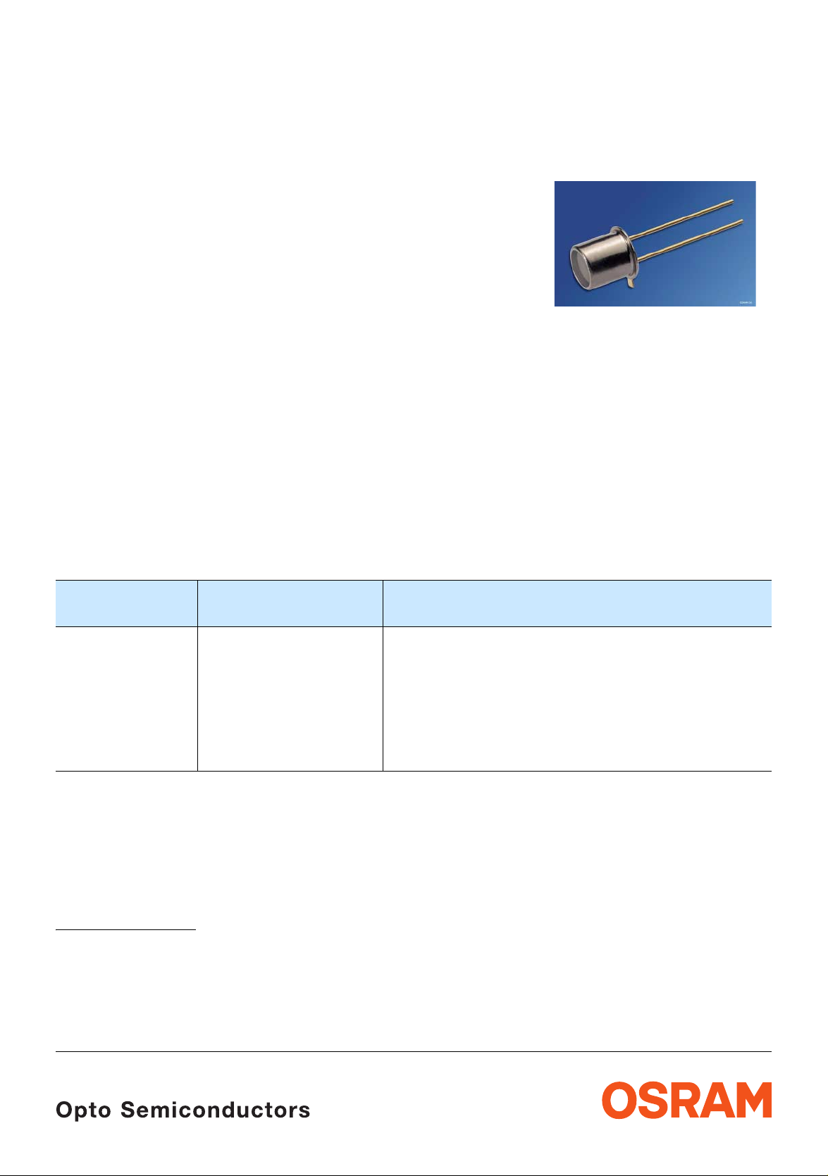
Silizium-PIN-Fotodiode
Silicon PIN Photodiode
Lead (Pb) Free Product - RoHS Compliant
BPX 65
Wesentliche Merkmale
• Speziell geeignet für Anwendungen im Bereich
von 350 nm bis 1100 nm
• BPX 65: Hohe Fotoempfindlichkeit
• Hermetisch dichte Metallbauform (TO-18),
geeignet bis 125
oC1)
Anwendungen
• Schneller optischer Empfänger mit groβer
Modulationsbandbreite
Typ
Type
Bestellnummer
Ordering Code
Features
• Especially suitable for applications from
nm to 1100 nm
350
• BPX 65: high photosensitivity
• Hermetically sealed metal package (TO-18),
suitable up to 125
oC1)
Applications
• Fast optical sensor of high modulation
bandwidth
Gehäuse
Package
BPX 65 Q62702P0027 18 A3 DIN 41870, planes Glasfenster, hermetisch
dichtes Gehäuse, Lötspieβe im 2.54-mm-Raster
(2/10”), Anodenkennzeichnung: Nase am
Gehäuseboden
18 A3 DIN 41870, flat glass lens, hermetically sealed
2
package, solder tabs 2.54 mm (
/10”) lead spacing,
anode marking: projection at package bottom
1)
Eine Abstimmung der Einsatzbedingungen mit dem
Hersteller wird empfohlen bei
1)
For operating conditions of TA > 85 °C please contact
us.
2007-04-02 1
T
> 85 °C.
A
Page 2
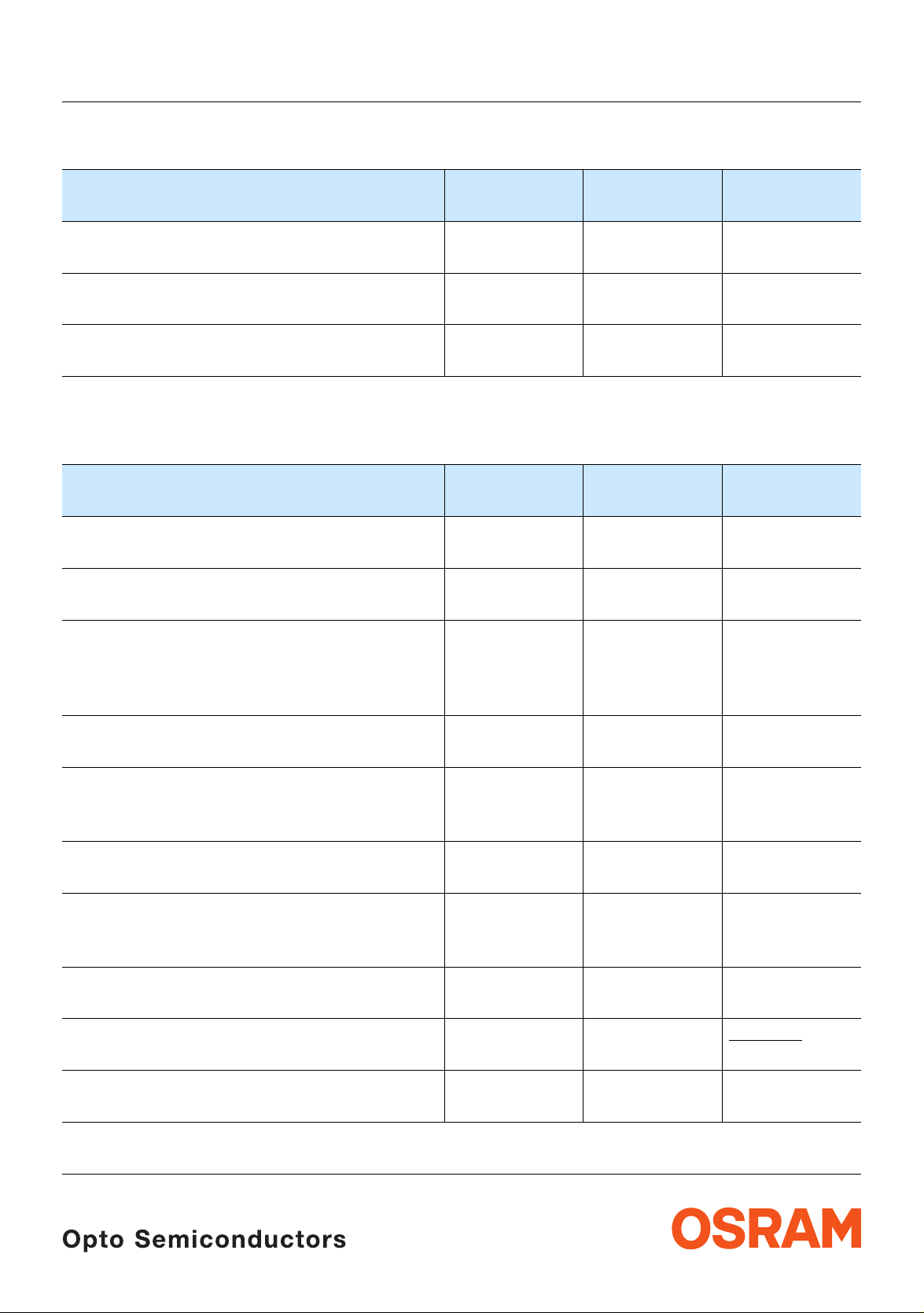
Grenzwerte Maximum Ratings
BPX 65
Bezeichnung
Parameter
Betriebs- und Lagertemperatur
Symbol
Symbol
T
; T
op
stg
Operating and storage temperature range
Sperrspannung
V
R
Reverse voltage
Verlustleistung, TA = 25 oC
P
tot
Total power dissipation
Kennwerte (TA = 25 °C, Normlicht A, T = 2856 K) Characteristics (TA = 25 °C, standard light A, T = 2856 K)
Bezeichnung
Parameter
Fotoempfindlichkeit, VR = 5 V
Symbol
Symbol
S
Spectral sensitivity
Wellenlänge der max. Fotoempfindlichkeit
λ
S max
Wavelength of max. sensitivity
Spektraler Bereich der Fotoempfindlichkeit
S = 10% von S
max
λ 350 … 1100 nm
Spectral range of sensitivity
S = 10% of S
Bestrahlungsempfindliche Fläche
max
A
Radiant sensitive area
Wert
Value
Einheit
Unit
– 40 ... + 125 °C
50 V
250 mW
Wert
Value
Einheit
Unit
10 (≥ 5.5) nA/Ix
850 nm
1.00 mm
2
Abmessung der bestrahlungsempfindlichen
Fläche
Dimensions of radiant sensitive area
Halbwinkel
L × B
L × W
ϕ ± 40 Grad
Half angle
Dunkelstrom
Dark current
V
= 20 V
R
Spektrale Fotoempfindlichkeit, λ = 850 nm
I
S
Spectral sensitivity
Quantenausbeute, λ = 850 nm
η 0.80 Electrons
Quantum yield
Leerlaufspannung, Ev = 1000 Ix
V
Open-circuit voltage
2007-04-02 2
1 × 1 mm²
deg.
R
λ
1 (≤ 5)
0.55 A/W
nA
Photon
O
320 (≥ 270) mV
Page 3
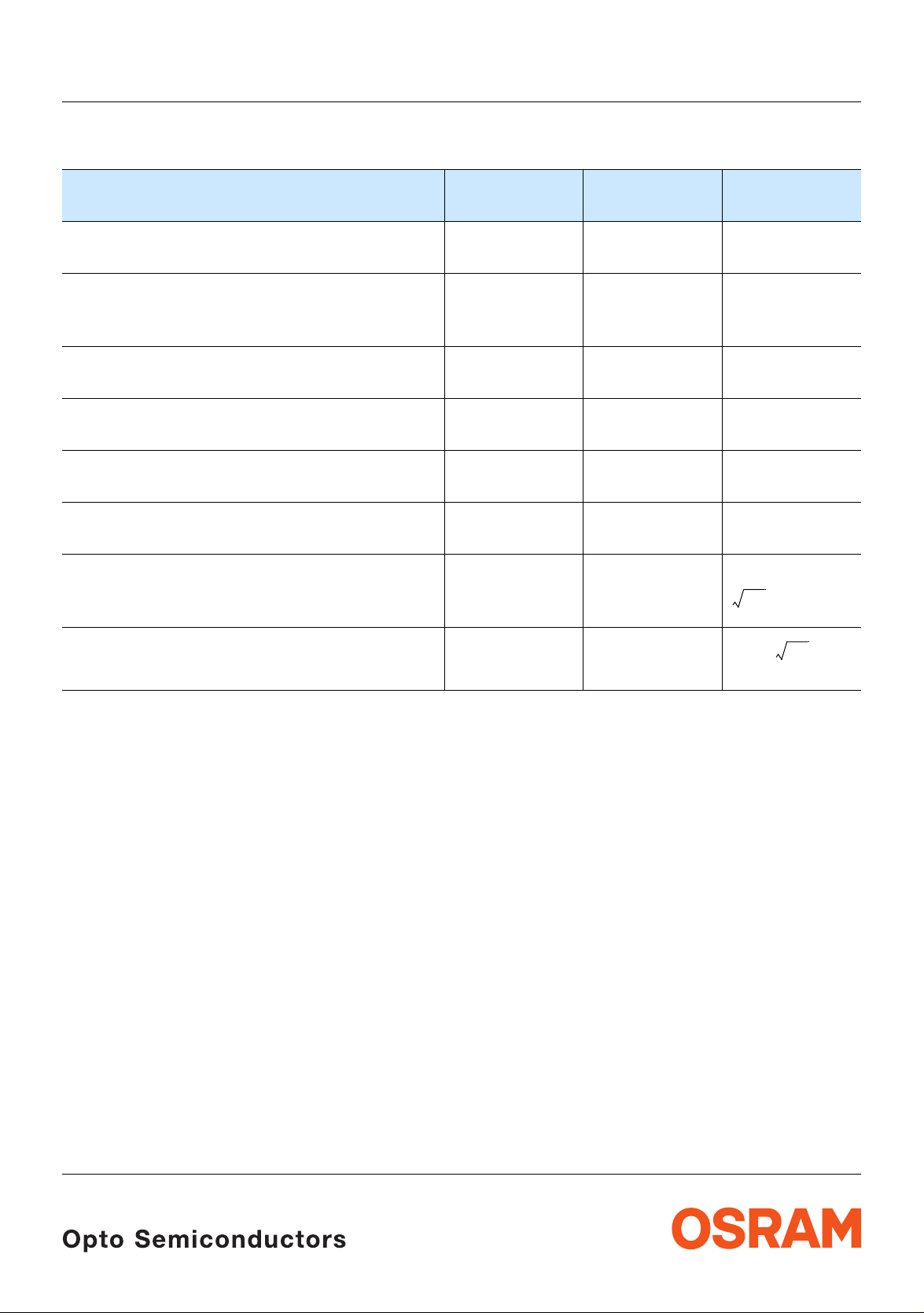
Kennwerte (TA = 25 °C, Normlicht A, T = 2856 K)
T
Characteristics (
= 25 °C, standard light A, T = 2856 K) (cont’d)
A
Bezeichnung
Parameter
Symbol
Symbol
Wert
Value
BPX 65
Einheit
Unit
Kurzschlussstrom, Ev = 1000 Ix
Short-circuit current
Anstiegs und Abfallzeit des Fotostroms
Rise and fall time of the photocurrent
R
= 50 Ω; VR = 5 V; λ = 850 nm; Ip = 800 μA
L
Durchlassspannung, IF = 100 mA, E = 0
Forward voltage
Kapazität,
V
R
= 0 V,
= 1 MHz,
f
E
= 0
Capacitance
Temperaturkoeffizient von V
Temperature coefficient of V
Temperaturkoeffizient von I
Temperature coefficient of I
L
L
K
K
Rauschäquivalente Strahlungsleistung
Noise equivalent power
V
= 20 V, λ = 850 nm
R
Nachweisgrenze, VR = 20 V, λ = 850 nm
Detection limit
I
SC
t
, t
r
V
F
C
0
TC
V
TC
I
NEP
f
10 μA
12 ns
1.3 V
11 pF
– 2.6 mV/K
0.2 %/K
3.3 × 10
D* 3.1 × 10
–14
12
W
----------- Hz
cm Hz×
--------------------------
W
2007-04-02 3
Page 4
BPX 65
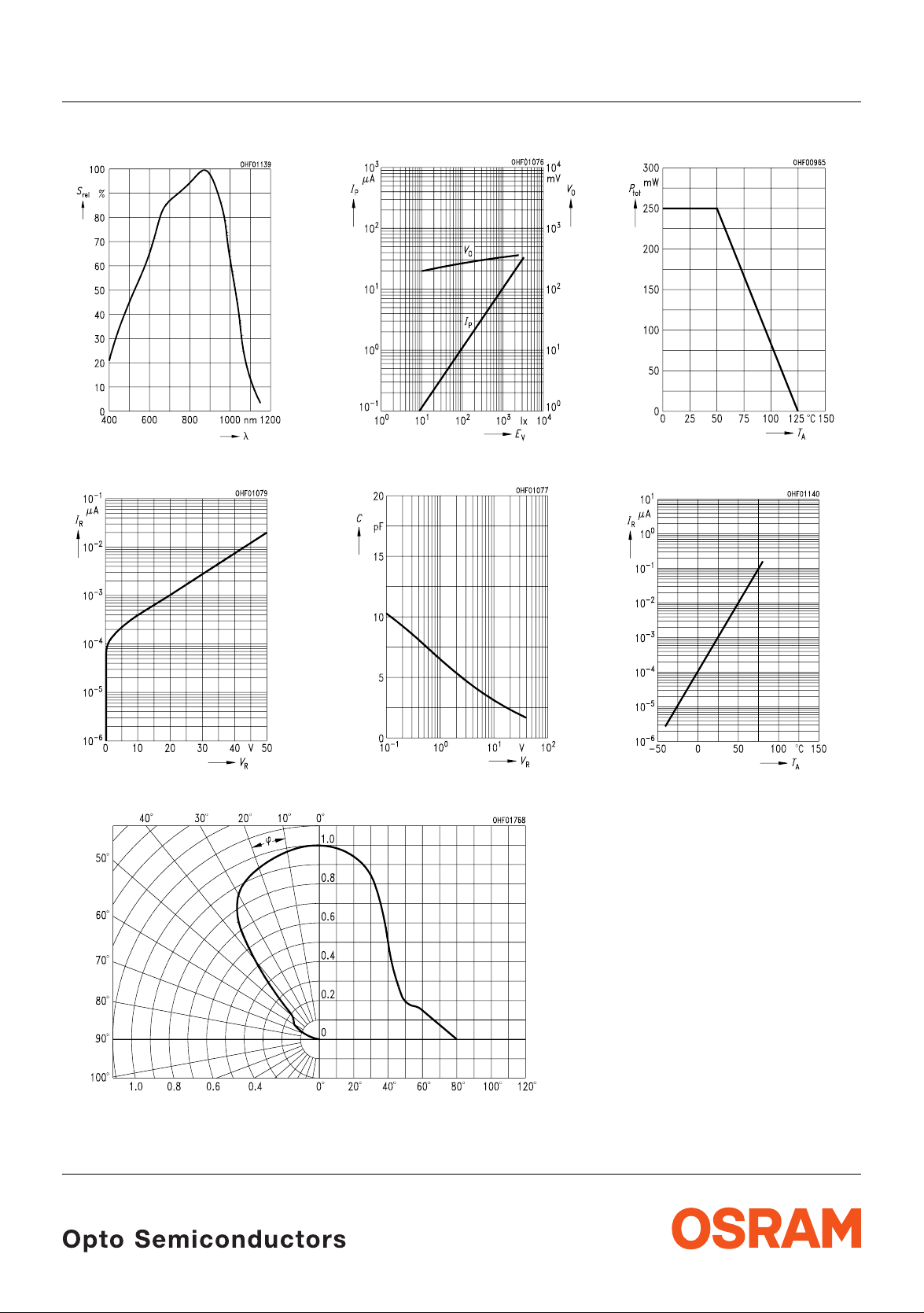
Relative Spectral Sensitivity
S
= f (λ)
rel
Dark Current
I
= f (VR), E = 0
R
Photocurrent IP = f (Ev), VR = 5 V Open-Circuit-Voltage VL = f (Ev)
Capacitance
C = f (V
), f = 1 MHz, E = 0
R
Total Power Dissipation
P
= f (TA)
tot
Dark Current
I
= f (TA), VR = 20 V, E = 0
R
Directional Characteristics
S
= f (ϕ)
rel
2007-04-02 4
Page 5
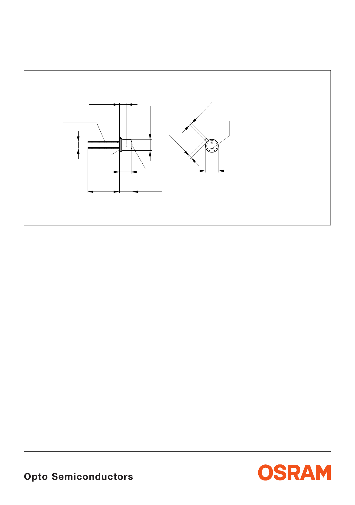
Maßzeichnung Package Outlines
BPX 65
(2.7 (0.106))
ø0.45 (0.018)
spacing
2.54 (0.100)
Maße in mm (inch) / Dimensions in mm (inch).
welded
5.3 (0.209)
5.0 (0.197)
14.5 (0.571)
12.5 (0.492)
Chip position
5.5 (0.216)
5.0 (0.197)
ø4.8 (0.189)
glass
lens
1.1 (0.043)
ø4.6 (0.181)
0.9 (0.035)
1.1 (0.043)
0.9 (0.035)
Anode
Cathode
ø5.6 (0.220)
ø5.3 (0.209)
= SFH 482
= SFH 402, BPX 65
(package)
GETY6013
2007-04-02 5
Page 6
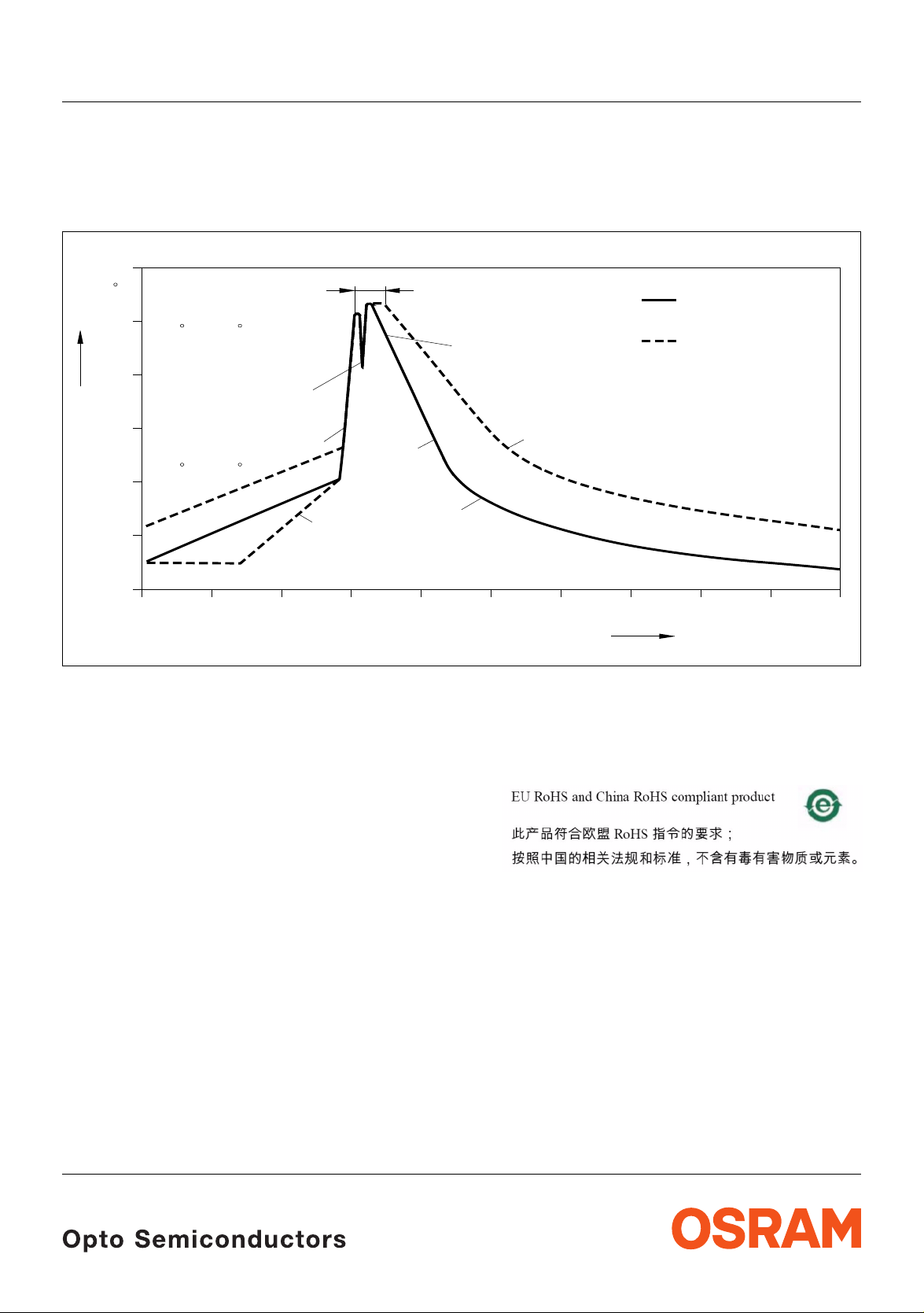
Lötbedingungen Soldering Conditions Wellenlöten (TTW) (nach CECC 00802) TTW Soldering (acc. to CECC 00802)
BPX 65
300
C
250
T
200
150
100
235 C
CC... 130100
50
0
0
C... 260
1. Welle
1. wave
ca 200 K/s
50 100 150 200 250
2 K/s
10 s
5 K/s
Zwangskühlung
forced cooling
2. Welle
2. wave
Normalkurve
standard curve
Grenzkurven
limit curves
2 K/s
t
OHLY0598
s
Published by
OSRAM Opto Semiconductors GmbH
Wernerwerkstrasse 2, D-93049 Regensburg
www.osram-os.com
© All Rights Reserved.
The information describes the type of component and shall not be considered as assured chara cteristics.
Terms of delivery and rights to change design reserved. Due to technical requirements components may contain
dangerous substances. For information on the types in question please contact our Sales Organization.
Packing
Please use the recycling operators known to you. We can also help you – get in touch with your nearest sales office.
By agreement we will take packing material back, if it is sorted. You must bear the costs of transport. For packing
material that is returned to us unsorted or wh ich we are not obliged to accept, we shall hav e to invoice you for any costs
incurred.
Components used in life-support devices or systems must be expressly authorized for such purpose! Critical
components
1
A critical component is a component used in a life-support device or sys tem whose failure can reasonably be expected
1
, may only be used in life-support devices or systems 2 with the express written approval of OSRAM OS.
to cause the failure of that life-support device or system, or to affec t its safety or e ffectiveness of that dev ice or system.
2
Life support devices or systems are intended (a) to be implanted in the h uman body, or (b) to support and/or maintain
and sustain human life. If they fail, it is reasonable to assume that the health of the user may be endangered.
2007-04-02 6
 Loading...