

Page 1
SERVICE MANUAL
MODEL NAME : MIS – 4201
Designed by Checked by Approved by
ORION PDP CO.,LTD
Page 2
*Revision History
Revision
No.
0 SEPTEMBER.
Revision Date Page Particulars of Revision
01 2005
Causes of
Revision
61 Service manual Establishment
2
ORION PDP CO.,LTD
Page 3

* Table of Contents
1. For Safe Service
2. Tools and Measuring
3. Service Procedure
4. Product Specification
5. Board Description
6. Wiring Diagram
7. Dismantling Procedure
8. Adjustment Method
9. How to Upgrade
10. Trouble Shooting
11. Parts Replacement and Related Details
12. Spare Parts List
13. Option List(Cables)
14. Explode View for MIS-4201
3
ORION PDP CO.,LTD
Page 4

1. For Safe Service
1-1. SAFETY PRECAUTIONS
MIS-4201 is a display device to be divided into a Panel part , a Drive part and a
mechanical part. The Panel part consists of Electrodes, Phosphor, various dielectrics and
gas, the Drive part includes electronic circuitry and Board and The mechanical part
includes mask assembly, back cover and other parts.
When using / handling this monitor, Please pay attention to the below warning and cautions.
Indicates a hazard that may lead to death or injury if the warning is ignored and the
product is handled incorrectly.
Indicates a hazard that can lead to injury or damage to property if the caution is ignored
and the product is handled incorrectly.
1-2. WARNING
1) Do not supply a voltage higher than that specified to this product.
This may damage the product and may cause fire.
2) Do not use this product in locations where the humidity is extremely high,
where it may be splashed with water, or where flammable materials surround it.
Do not install or use the product in a location that does no satisfy the specified
environmental conditions.This may damage the product and may cause a fire.
3) If a foreign substance (such as water, metal, or liquid) gets inside the product,
immediately turn off the power. Continuing to use the product, it may cause fire or
electric shock.
4) If the product emits smoke, and abnormal smell, or makes an abnormal sound,
immediately turn off the power. Continuing to use the product, it may cause fire or
electric shock.
5) Do not disconnect or connect the connector while power to the product is on.
It takes some time for the voltage to drop to a sufficiently low level after the power has
been turned off.Confirm that the voltage has dropped to a safe level before
disconnecting or connecting the connector.
6) Do not pull out or insert the power cable from/to an outlet with wet hands.
It may cause electric shock.
7) Do not damage or modify the power cable. It may cause fire or electric shock.
8) If the power cable is damaged, or if the connector is loose, do not use the product:
otherwise, this can lead to fire or electric shock.
9) If the power connector or the connector of the power cable becomes dirty or dusty,
wipe it with a dry cloth. Otherwise, this can lead to fire.
10) MIS-4201 set uses a high voltage (Max.450V DC). Keep the cautions concerning
electric shock and do not touch the Device circuitry when handling the PDP Unit.
And because the capacitor of the Device circuitry may remain charged at the
moment of Power OFF, standing by for 1 minute is required in order to touch the
Device circuitry
4
ORION PDP CO.,LTD
Page 5

.
11) In order to protect static electricity due to C-MOS circuitry of the Drive part, wear a
wrist band to protect static electricity when handling.
12) When cleaning the Panel, wipe it with a soft cloth moistened with water or neutral
detergent, be careful not to touch the connector part of the Panel. And don’t use
chemical materials like thinner or benzene.
13) If this product is used as a display board to display a static image, “image sticking”
occurs. This means that the luminance of areas of the display that remain lit for a
long time drops compared with luminance of areas that are lit for a shorter time,
causing uneven luminance across the display.
The degree to which this occurs is in proportion to the luminance at which the
display is used. To prevent this phenomenon, therefore, avoid static images as
much as possible and design your system so that it is used at a low luminance, by
reducing signal level difference between bright area and less bright area through
signal processing.
14) Because PDP Module(set) emits heat from the Glass Panel part and the Drive
circuitry, the environmental te mperature must not be over 40°C. the temperature of
the Glass Panel part is especially high owing to heat from internal Drive circuitry.
And because the PDP Module(set) is driven by high voltage, it must avoid
conductive materials.
15) When inserting components or circuit board in order to repair, be sure to fix a lead
line to the connector before soldering.
16) When inserting high-power resistor(metal-oxide film resistor or metal film resistor)
in order to repair, insert it as 10mm away as from a board.
17) During repairs, high voltage or high temperature components must be put away
from a lead line
18) This is a Cold Chassis but you had better use a cold transformer for safety during
repairs. When repairing electricity source part, you must use the cold transformer.
19) Do not place an object on the glass surface of the display. The glass may be broken
or be scratched.
20) This product may be damaged if it is subject to excessive stresses
(such as excessive voltage, current, or temperature).
The absolute maximum ratings specify the limits of these stresses.
21) The recommended operating conditions are conditions in which the normal
operation of this product is guaranteed. All the rated values of the electrical
specifications are guaranteed within these conditions.
Always use the product within the range of the recommended operating conditions.
Otherwise, the reliability of the product may be degraded
22) This product has a glass display surface. Design your system so that excessive
shock and load are not applied to the glass. Exercise care that the vent at the
corner of the glass panel is not damaged.
If the glass panel or vent is damaged, t he product is inoperable.
5
ORION PDP CO.,LTD
Page 6

.
23) Do not cover or wrap the product with a cloth or other covering while power is
supplied to the product.
24) Before turning on the power to the product, check the wiring of the product and
confirm that the supply voltage is within the rated voltage range. If the wiring is
wrong or if a voltage outside the rated range is applied, the product may
malfunction or be damaged.
25) Do not store this product in a location where temperature and humidity are high.
This may cause the product to malfunction. Because this product uses a discharge
phenomenon, it may take time to light (Operation may be delayed) when the
product is used after it has been stored for a long time. In this case, it is
recommended to light all cells for about 2 hours (aging).
26) This product is made from various materials such as glass, metal, and plastic.
When discarding it, be sure to contact a professional waste disposal operator.
27) If faults occur due to arbitrary modification or disassembly, Orion PDP Co. ,Ltd..is
not responsible for function, quality or other items.
28) Use of the product with a combination of parameters, conditions, or logic not
specified in the specifications of this product is not guaranteed. If intending to use
the product in such a way, be sure to consult Orion PDP Co.,Ltd. in advance.
29) Within the warranty period, general faults that occur due to defects in components
such as ICs will be rectified by Orion PDP Co Ltd. However,
IMAGE STICKING due to misapplying the above (12) provision is not included in
the warranty. Repairs due to the other faults may be charged depending on
responsibility for the faults.
6
ORION PDP CO.,LTD
Page 7
2. Tools and Measuring
1) Portable Oscilloscope
2) Digital Multi-Meter (DMM)
3) (+) type adjustment bar
4) (+) type screw driver and tip
5) Hexagonal screw driver
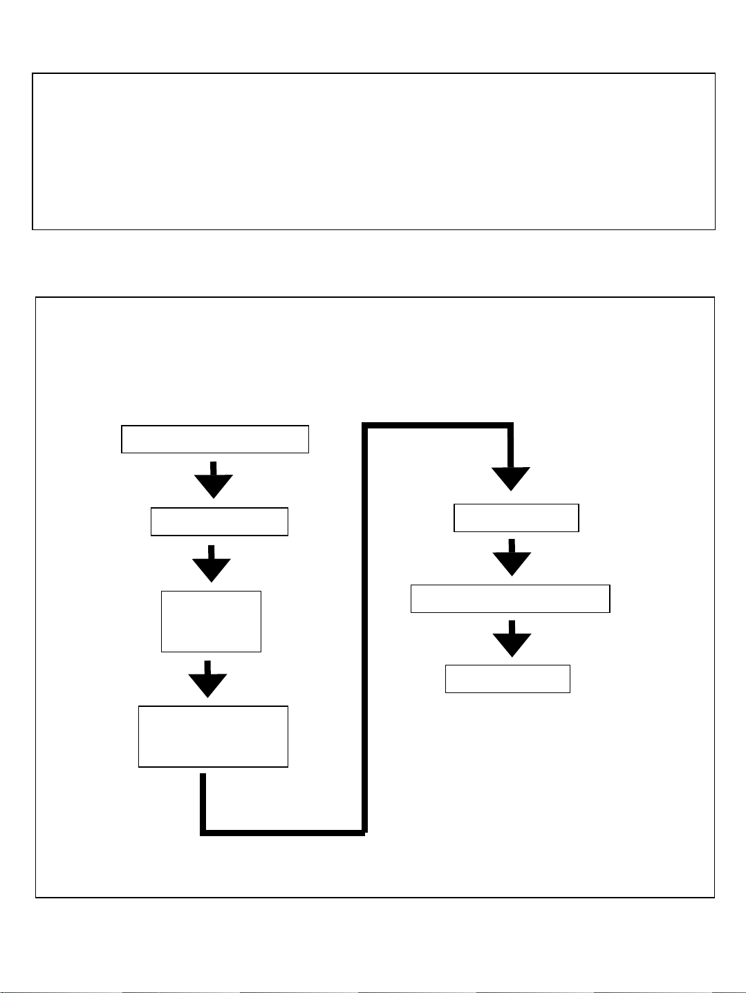
3. Service Procedure
MIS-4201 service is carried out in the following order.
For service procedures and methods of each part,
refer to the corresponding section in this manual.
Preliminary Inspection
Set Dismantling
Diagnosis,
Repair,
Upgrade
Adjustment and
Operation Status
Check
Set Assembly
Operation Status Check
Completion
7
ORION PDP CO.,LTD
Page 8
4. Product Specification
4-1. General Specification
FEATURE SPECIFICATION REMARK
POWER INPUT AC 100V ~ 240V , 50/60 Hz
POWER
CONSUMPTION
DIMENSIONS
WEIGHT 27Kg MONITOR BODY ONLY
SCREEN SIZE 921mm[H]×518mm[V] DIAGONAL IS 42 INCH
ASPECT RATIO 16 : 9
RESOLUTION 853[H]×480[V]
PIXEL PITCH 1.08 mm × 1.08 mm
COLOR
ARRAGEMENT
NUMBER OF
GRADATION
400W [MAX]
925mm[W]×523mm[H]×76.5m
m[D]
RGB VERTICAL STRIPE TYPE
256 STEPS FOR VIDEO,RGB
FULL WHITE 100%
LEVEL
WIDE VGA[1pixel=3 RGB
cells]
PEAK BRIGHTNESS Min.≥ 200 cd/㎡ 1 % WINDOWS
CONTRAST RATIO Min.≥ 400 : 1 DRCR
SEAM ≤ 6mm Monitor to Monitor
VIEWING ANGLE 160 deg.
CONTROL TIME
INTERVAL
FRONT FILTER
8
≥ 10 SECOND MSCS CONTROL
LOW REFLECTION COATING
FILM
ORION PDP CO.,LTD
Page 9
4-2. Input & Output Terminal
PORT
NAME
COMPOSI
TE
[VIDEO]
S-VIDEO NTSC/PAL/SECAM
COMPON
ENT
[DVD/DTV]
PC ANALOG RGB
NTSC/PAL/SECAM BNC 1
Y,Pb/Cb,Pr/Cr
720P[50/60Hz]
1080i[50/60Hz]
*VGA
*SVGA
*XGA
*UXGA[1600*1200,60Hz]
PORT SPEC.
* DVD : 480i,576i
* DTV : 480P,576P
INPUT PORT OUTPUT PORT
PORT
TYPE
PIN
DIN 4
PIN
BNC 3
PIN
D-SUB
15 PIN
Q’ty
1
1
1
1
PORT
TYPE
BNC 1
PIN
DIN 4
PIN
BNC 3
PIN
D-SUB
15 PIN
Q’ty
REMARK
1
1
1
1
DVI DIGITAL RGB [TMDS]
*VGA
*SVGA
*XGA
*UXGA[1600*1200,60Hz
REMOTE
CONTROL
RS-232C
*FEMALE : INPUT
*MALE : OUTPUT
9
DVI-D
24 PIN
D-SUB
9 PIN
1 *
1STRAIG
DVI-D
24 PIN
D-SUB
9 PIN
1
OPTION
HDCP
1
HT TYPE
[NOT
TWIST]
ORION PDP CO.,LTD
Page 10
4-3. Input Signal Specification
No Item Min
Component
(DVD /
D-TV)
1
DVI DVI Input
2
PC
(ANALOG
RGB)
3
Component
Input Terminal
Y Input Level
Sync Level 0.24 0.3 0.36 Vpp
Pb Input Level ± 350 mV
Pr Input Level ± 350 mV
Terminal
RGB Input Level 0.5 0.7 1.0 Vpp
Sync Separate 2.5 5.0 Vdc
Sync Composite 2.5 5.0 Vdc
Component Input
Y, Pb, Pr (Green, Blue, Red)
0.6 0.8 0.8 Vpp
DVI-D Terminal
Digital R,G,B(TMDS)
Vcc(Termination Supply Vol.)
=3.3V, ±5%
Termination Resistance :
50Ohms, ±10%
Typ
e
Max Unit Remark
4
5
Composite
Video
S-Video
10
Sync On Green 0.2 0.3 0.4 Vpp Negative
Sync
Video Input
Terminal
Video Input Level 0.85 1.0 1.15 Vpp
Video Sync Input 0.25 0.30 0.35 Vpp
Video burst Input 0.25 0.30 0.35 Vpp
S-Video Input
Terminal
NTSC Y=1Vp-p/75ohm, C=0.286Vp-
PAL Y=1Vp-p/75ohm, C=0.299Vp-
BNC Jack
4 PIN DIN Jack
p/75ohm
p/75ohm
ORION PDP CO.,LTD
Page 11
5. Board Description
5-1. I/P PCB
For input signal, S-video signal to separately enter luminance and color
signals, Y/C composite video signal, DVD signal, DTV signal and the
graphic signals of analog RGB and digital RGB can be used. In case of
graphic signals, both analog and digital versions use AD9887 ADC.
Each of 3CH even/ odd signals are converted into 8bit signals and
entered to scaler. Similarly, DTV signals are also entered to scaler
through the same route. Video signals are converted to the digital format
of BT601 through the video processor of VPC3230D. Among input
signals, CVBS (only NTSC) is entered to VPC3230D as Y/C is
separated through 3D-comb filter. VPC3230D converts the format of
input signals into 16-bit BT601, thus enters them to the deinterlacer of
MDIN-150. MDIN-150 converts interface signal into progressive to send
signal output to scaler. The output signal format is BT601, that is, Y:U:V
4:2:2 16bit. Scaler receives the input of MDIN-150 from control of
CPU[RDC R2021] and graphic signal from AD9887, thus administers
scaling to the resolution of multi-panel [853*480] and produces signal
output in LVDS format.
11
ORION PDP CO.,LTD
Page 12
5-2. DIGITAL PCB
DIGITAL PCB receives the following signals and data from IP Board.
*LVDS FORMAT
- R, G, B data - DCLK
- Enable - H Sync.
- V Sync. - etc.
The data of R, G, B received from IP PCB is processed and adjusted to be
displayed in PDP through CON PCB and COF (Data drive circuit. )
DIGITAL PCB also has APL(Automatic Power Limit) circuit which controls
the power consumption and the heat in the PDP.
The data of H Sync, V Sync and DCLK is converted to X, Y & Z Timing pulse
data for PDP.
It is also working to reduce the Dynamic false contour and to maximize the
256 Gray level.
Test Pattern Switch for Module Inspection
[High : ON]
12
ORION PDP CO.,LTD
Page 13
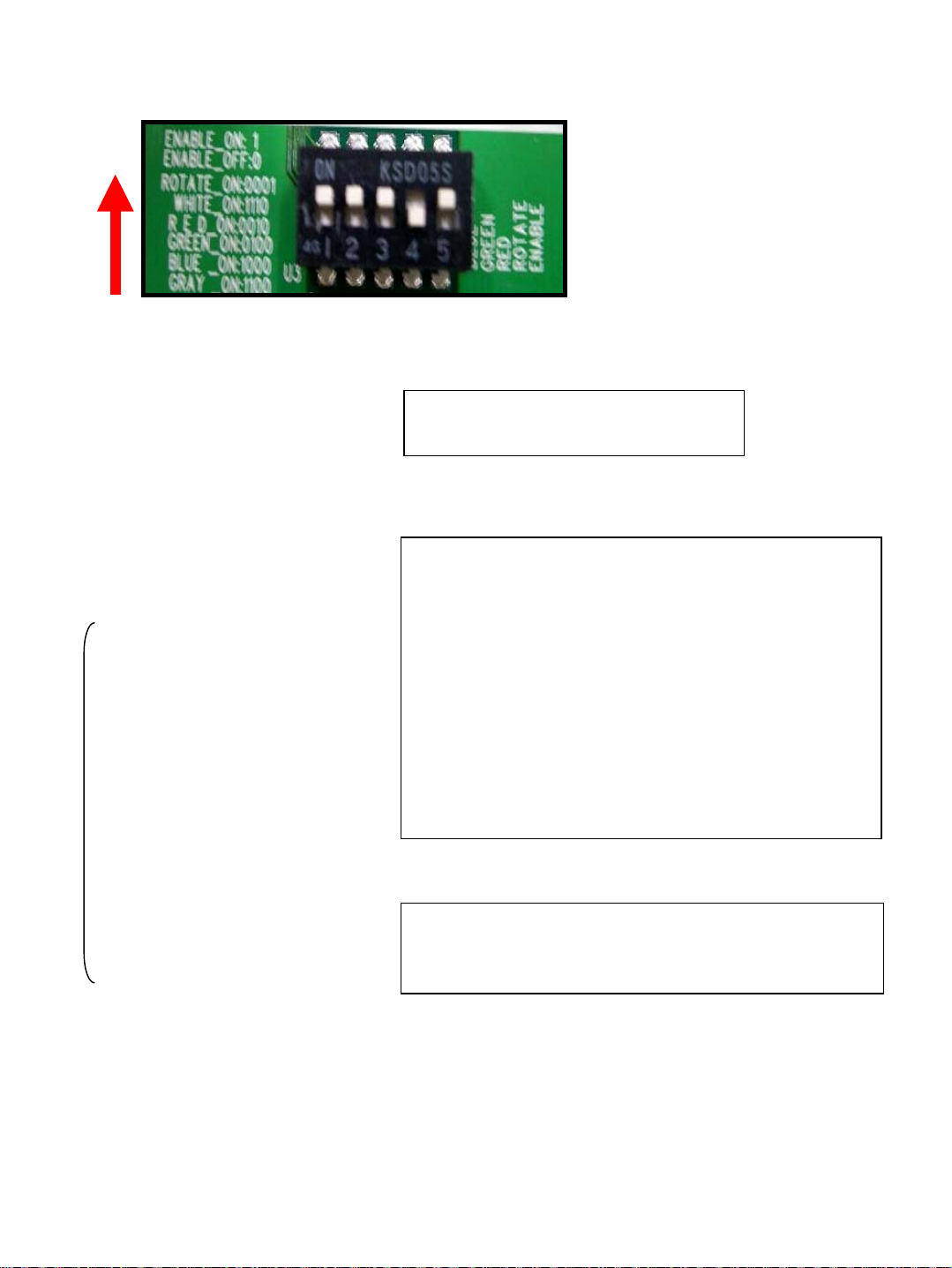
5-2-1. How to use Inner Pattern Switch on DIGITAL PCB
ON
1
[Inner Pattern Switch on DIGITAL PCB
0
※ SET NO : 1 2 3 4
- WHITE : 1 1 1 0
- RED : 0 0 1 0
- GREEN : 0 1 0 0
- BLUE : 1 0 0 0
- GRAY : 1 1 0 0
- ROTATE : 0 0 0 1
WHITE
↓
As an example,
white pattern
5 : Enable ON - 1
Enable OFF - 0
*If you want to use this inner pattern switch on
DIGITAL PCB, the switch of CN801 on POWER
PCB should be set as shown next page.
RED
↓
YELLOW
↓
GREEN
↓
CYAN
↓
BLUE
↓
MAGENTA
13
If the switch [CN801] on POWER PCB is
connected, you can turn the power on & off
ORION PDP CO.,LTD
Page 14
5-2-2. How to use switch on POWER PCB
[PLANK TYPE]
1 2 3 4 5 6 7
5Vst_by
CN801
1:ACD
2:RELAY_ON
3:5Vst_by
4:GND
5:Vs_ON
6:5VD
7:NC
RELAY_ON
Vs_ON
SWITCH DIAGRAM
HIGH LOW
[Turn Off]
HIGH LOW
[Turn On]
14
ORION PDP CO.,LTD
Page 15
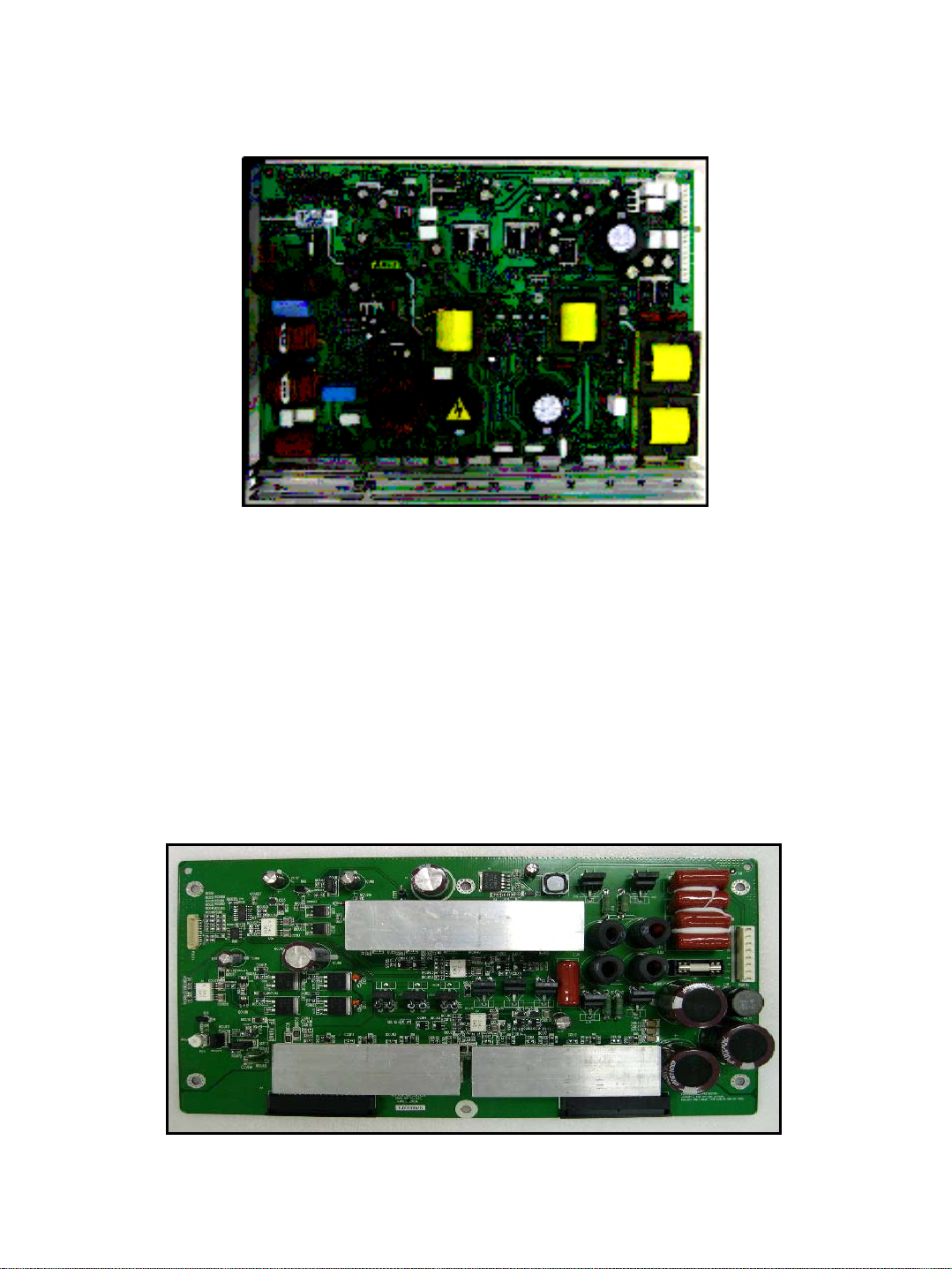
5-3. POWR PCB
POWER PCB is to receive the AC power outside and to send the power each
PCB in MIS-4201. AC 100 ~ 240 V ± 10% & 50/60 Hz ± 1 Hz is available.
5-4. SUS X PCB
SUS X PCB consists of the following.
- SUSTAIN : It includes the circuits of Energy recovery and discharge.
- V_SHELF power REGULATOR : It works for adjusting and keeping the
Voltage in the panel.
- 15V REGULATOR : It is changing from the 5V received from POWER PCB
to the 15V and supplying it to Drive IC and SUS Y PCB.
15
ORION PDP CO.,LTD
Page 16
5-5. SUS Y PCB
SUS Y PCB consists of the following.
-SUSTAIN -RAMP-DOWN
-Y-SHELF -Y-ERASE
-SCAN -RAMP-UP REGULATOR
-SCAN REGULATOR -15V REGULATOR
SUSTAIN includes the circuits of Energy recovery and discharge.
The others work for adjusting and keeping the voltage sending to Panel.
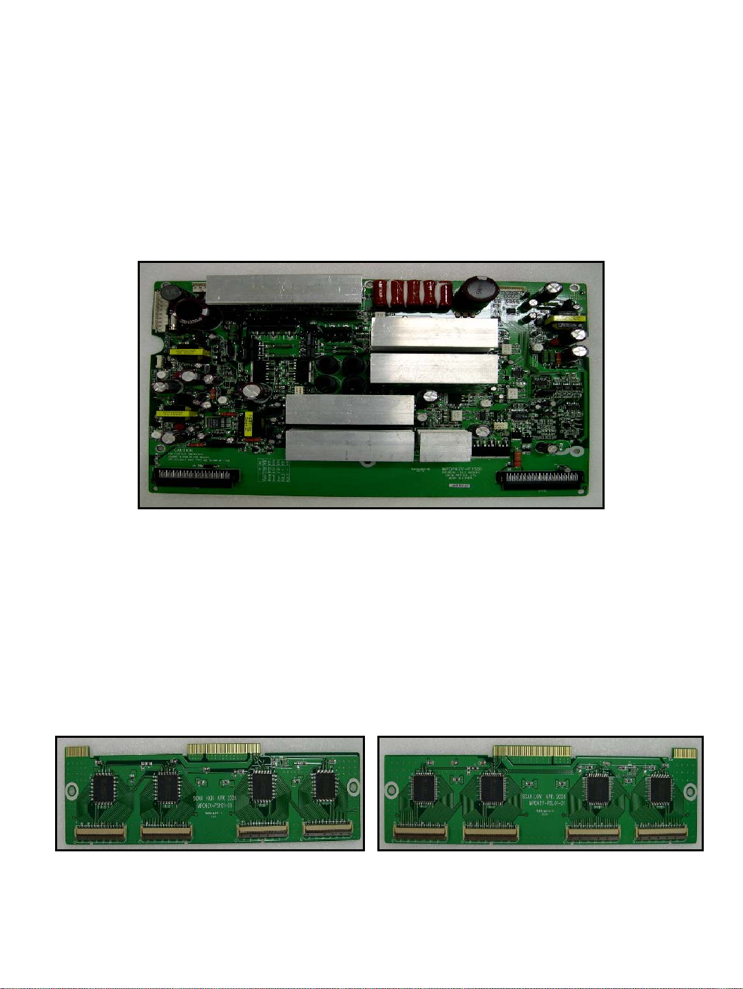
5-6. SCAN HIGH / LOW PCB
The SCAN HIGH and LOW PCB consist of 4 PDP Scan Driver IC.
Driver IC controls 65 of high current and high voltage of output by using the
65 bit cascadable 8MHz shift register. Additionally, 64 or 65 bit of output
may be used depending on input values into the SEL port. Driver IC is
supplied with the 150V power output and the 5V logic power separately.
Command inputs are compatible with CMOS.
16
ORION PDP CO.,LTD
Page 17
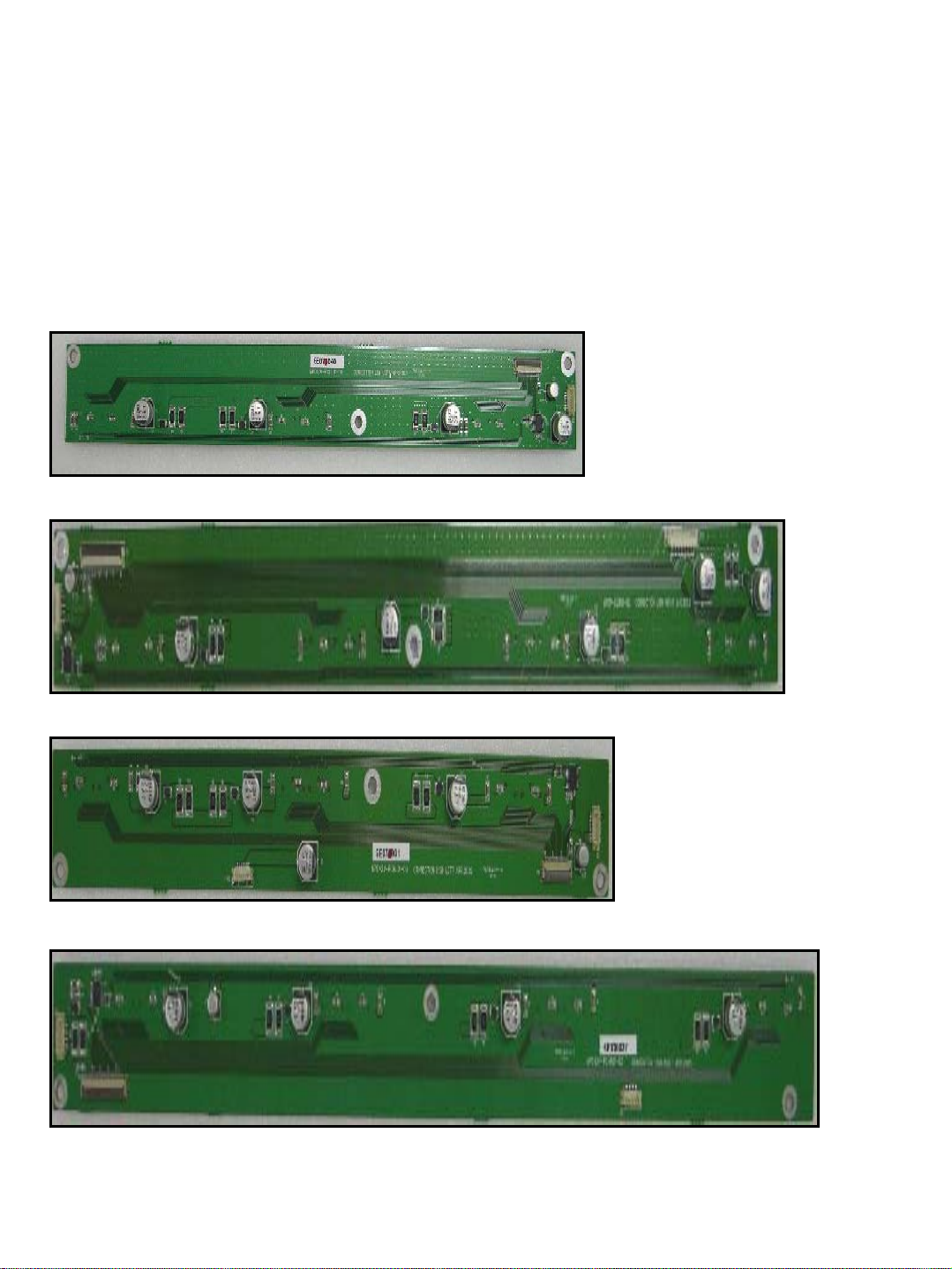
5-7. CON HIGH LEFT & RIGHT / CON LOW LEFT & RIGHT PCB
The CON HIGH LEFT & RIGHT / CON LOW LEFT & RIGHT PCB are
connecting the data signal from SUS Y PCB with Z(data) Driver IC which is
attached to the Panel.
The CON HIGH LEFT & RIGHT / CON LOW LEFT & RIGHT PCB are
connected to totally 7 COF(Chip On Film).
COF consists of the DATA Driver IC.
Those 7 COF having 2559 lines are connected with Panel.
CON LOW LEFT(LL) PCB
CON LOW RIGHT(LR) PCB
CON HIGH LEFT(HL) PCB
CON HIGH RIGHT(HR) PCB
17
ORION PDP CO.,LTD
Page 18
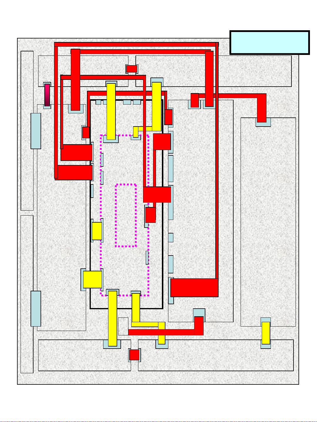
6. Wiring Diagram [Signal Line & Power Line]
*Yellow : signal line
*Red : power line
CON HIGH LEFT
CON HIGH RIGHT
④
P201A
P6
SCAN HIGH
①
P2
⑤
P1
P6
⑧
⑨
⑥
P4
J6
J3
JJ2
JL1
JN1
P5 P6
⑫
IP
BOAR
D
H1
52
ID
7
ID2
7
①
JC1JC
2
P302
P7
⑪
⑦
⑥
④
CN808
CN805
CN807
CN804
⑤
CN806
POWER
SUS Y
P1O2A
SCAN LOW
CON LOW LEFT CON LOW RIGHT
⑩
JP1
③
DIGITAL
U2
H141
H151 P304
⑫
AC
P4
P5
①
PA301A
U4
⑪
P6
⑦
⑧
P7
SUS X
CN803
CN809
CN802
CN80
1
⑨
CN101
P2021A
⑬
②
P5
18
ORION PDP CO.,LTD
Page 19
*A]The specification of connection
No.
①
②
③
④
⑤
⑥
MATERIAL
NUMBER
M7506149
M7506150
M7506151
M7506148
M7506146
M7506147
MATERIAL NAME SPECIFICATION
CONNECTOR CABLE 6P12505HS-
06+12505TS+ULW=50
CONNECTOR CABLE
12P
CONNECTOR CABLE
15P
CONNECTOR CABLE
8P
CONNECTOR CABLE
10P
CONNECTOR CABLE
4P
12505HS-
12+12505TS+ULW=90
12505HS-
15+12505TS+ULW=90
YH396-08V+YT396J+ULW=400 1 EA X_SUS
YH396-10V+YT396J+ULW=400 1 EA Y_SUS
YH396-04V+YT396J+ULW=300 1 EA Y_5V
Q’
TY
UNIT
3EA
1EAX~CON
1EAY~DIG.
REMAR
K
CON~
CON,Y
M7506155
⑦
M7506143
⑧
M7506154
⑨
M7506145
⑩
M7519752 FFC 50P 100L 0.5pt SINGLE SIDE 2 EA
⑪
M7519753 FFC 30P 80L 0.5pt SINGLE SIDE 2 EA
⑫
M7519247 NOISE FILTER 02P-210M(TDK)-INLET(D)
⑬
CONNECTOR CABLE
4P
CONNECTOR CABLE
10P
CONNECTOR CABLE
6P
CONNECTOR CABLE
31P
171822-08+170262-1=100 1 EA DIG._5V
SMH250-10+LH01-250-12=460 1 EA AV-POW
SMH250-06+LH01-250-07=590 1 EA AV-POW
GT121-31S-CD+GT121-C-
15000=120
19
1EAAV-DIG
1EA
ORION PDP CO.,LTD
Page 20
7.Dismantling Procedure
7-1. Dismantling of Back Cover
GREEN CIRCLE
M4×8 : 4EA
Handle
RED CIRCLE
M4×5 : 32EA
1) Materials Used
M7543053 SCREW MACHINE M4×8 BIND MFZN 4EA
M7543073 SCREW MACHINE M4×5 BIND MFZN 23EA
2) Dismantling Procedure
① Remove 4 screws to fasten handle.
② Remove edge screws first, then continue on
to remove other screws.
③ Lift up back cover as
shown in the picture to
the left. Then, remove
J3 and J6 connectors.
④ After removing the cable
tie, remove fan cable.
Back
Cover
20
ORION PDP CO.,LTD
Page 21

7-2. Dismantling of I/P Plate Assembly
ⓐConnector
Dismantling Position
CN01
FIG22]Before I/P PCB
Dismantling
IP
Assembly
Screw
CN01
GN
D
GND
FIG23] I/P ASSEMBLY
FIG24] After I/P PCB Dismantling
FIG24]I/P Plate+Noise
1) Materials Used
M7543061 SCREW MACHINE PSW M3×8 MFZN 9 EA
2) Dismantling Procedure
① Dismantle connector in magenta circle of ⓐ in Fig. 22].
② Remove 4 screws in yellow circle of ⓑ in Fig. 22].
③ Dismantle CN01 connector of ⓒ in Fig. 22].
④ Remove 2 screws of GND of ⓓ in Fig. 22].
⑤ Remove I/P PCB from the dismantled IP assembly[Fig. 23].
Remove 5 screws in red circle.
⑥ Dismantled up to the status indicated in Fig. 24].
21
Filter Ass’y
ORION PDP CO.,LTD
Page 22

7-3. Dismantling of Support Bracket
Support Bracket
1) Materials Used
M7543053 SCREW MACHINE BIND M4×8 MFZN(BLACK) 8 EA
2) Dismantling Procedure
① Remove 4 fixing screws on the right.
② Remove 4 fixing screws on the left.
22
ORION PDP CO.,LTD
Page 23

7-4. Dismantling of Master Frame
1) Materials Used:
M7543053 SCREW MACHINE BIND M4×8 MFZN(BLACK) 10 EA
2) Dismantling Procedure (Refer to the above picture indicating the screws to
be removed.)
There is no particular order of dismantling. However, make sure to remove
all 10 screws. The below picture indicates the pure module status after
dismantling master frame.
23
ORION PDP CO.,LTD
Page 24

7-5. Dismantling of Wires
1) Dismantling Procedure:
When dismantling wires, make sure to dismantle all of the 13 varieties
without any specific order.
During assembly, take caution not to cause damage to connectors. Refer
to 6. Wiring Diagram (Signal & Power line) for wire connection.
2) The below picture shows wires dismantled from the above picture.
24
ORION PDP CO.,LTD
Page 25

7-6. Dismantling of SCAN PCB
1) Materials Used:
M7543061 SCREW MACHINE PSW M3×8 MFZN 4 EA
2) Dismantling Procedure (Refer to above picture for screwed to be removed.)
Remove all 4 screws without any specific order. The picture below shows
the process of FPC dismantling after removing screws.
25
ORION PDP CO.,LTD
Page 26

7-6-1. Tips for disassembling
1) SCAN LOW & HIGH PCB
FPC
Picture 1. Not recommended
2) CON LOW/LEFT & RIGHT PCB
Picture 2. Recommended
COF
Picture 1. Not recommended Picture 2. Recommended
<Attention> As Picture 1, it is not recommended taking out FPC and COF from PCB
Connector horizontally. As Picture 2, hold Scan PCB Connector as pictured and pull
down the PCB and take out FPC and COF.
3) CON_HIGH/LEFT & RIGHT PCB
: The same is recommended as CON LOW/LEFT & RIGHT PCB
26
ORION PDP CO.,LTD
Page 27

7-7. Dismantling of SUS Y PCB
1) Materials Used:
M7543051 SCREW MACHINE PSW M3×8 MFZN 7EA
2) Dismantling Procedure(Refer to above picture for screws to be removed.)
Remove all 7 screws without any specific order.
27
ORION PDP CO.,LTD
Page 28

7-8. Dismantling of SUS X PCB
1) Materials Used:
M7543061 SCREW MACHINE PSW M3×8 MFZN 6EA
2) Dismantling Procedure (Refer to above picture for screws to be removed.)
Remove all 6 screws without any specific order.
The below picture shows the process of FPC dismantling after removing
screws.
28
ORION PDP CO.,LTD
Page 29

7-9. Dismantling of DIGITAL / POWER PCB
1) Materials Used:
M7543061 SCREW MACHINE PSW M3×8 MFZN 12EA
2) Dismantling Procedure (Refer to above picture for screws to be removed.)
Remove all 12 screws without any specific order.
29
ORION PDP CO.,LTD
Page 30

7-10. Dismantling of CON PCB
1) Materials Used:
M7543061 SCREW MACHINE PSW M3×8 MFZN 20EA
2) Dismantling Procedure (Refer to above picture for screws to be removed.)
Remove all 12 screws without any specific order.
The below picture shows the process of COF dismantling. The process is
the same as of SUS Y PCB FPC dismantling.
30
ORION PDP CO.,LTD
Page 31

8. Adjustment Method
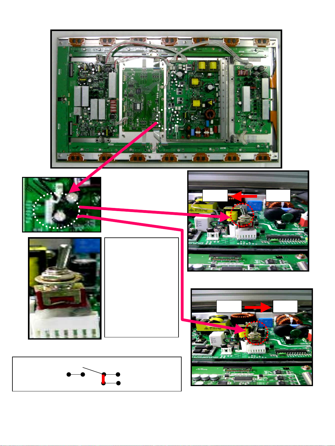
8-1. Voltage Adjustment
1) Measurement instruments
① Multi test signal such as BSG-360A and BSG-265L or equivalent
② Color Analyzer such as CA-100 or equivalent
③ Millimeter (acceptable tolerance is 0.5%)
④ Computer: The following is recommended.
SXGA(Resolution: 1024 * 768,60Hz) True color 16 Bit
2) Power Board Adjustment
1) Factors for adjustment
TP
CN 808/CN806
VR301
For Vsus Adjustment
VR :Variable Resistor
TP : Test Point
For Vadd Adjustment
2) Voltage adjustment
-Turn on the SET by MSCS Control.
-Select the Input of Your Using Signal
-Set the voltage as written on the
back-plate, refer to Fig1].
Min Type Max Preset TP
Vsus 180V 190V
Vadd 65V 70V
195V 190V
VR401
70V75V
Fig1]The voltage label
On the back plate
CN808 #1 PIN
CN806 #1 PIN
31
ORION PDP CO.,LTD
Page 32

3. Y Board Adjustment
1) Factors of Adjustment
ΔRamp-Down : To be indicated as ΔRamp-Dn
2) Voltage adjustment
After Power board voltage adjustment, Y Board voltage is to be
adjusted.Adjust the voltage as written on the back plate refer to fig1].
Ramp Up & Ramp Down should not be adjusted because it is possible
with Oscilloscope .But You Set a Center of Each VR’s Variable Range.
RY9
Adj-Vramp
RY33
TP_Vramp
LY28
TP_Vscan
RY16
Adj-Vshelf
LY31
TP_Vyer
LY10
TP_Vshelf
RY8
Adj-Vscan
32
RY18
Adj-Vyer
RY2
Adj-ramp_up_T
RY10
Adj-ramp_down_T
ORION PDP CO.,LTD
Page 33

Vyer Vy_shelf Vy_scan Vramp_up
ΔRamp-
Up
ΔRamp-Dn
Min 170V 80V 210V 40usec
Type 175V 85V 215V 145usec
115V
Max 180V 90V 230V 230usec
Preset 175V 85V CENTER
VR RY18 RY8 RY9 RY2 RY10
TP LY31 LY28 -
~
120V
Fixed
Voltage
215V
RY33
70usec
80usec
CENTER
-
110usec
4. X Board adjustment
1) Factors of adjustment.
RCU70
Adj_Vxshelf
LCU 1
TP_Vxshelf
2) Voltage adjustment
After Y board voltage adjustment, X Board voltage is to
be adjusted.Adjust the voltage as written on the back plate’s
label
33
ORION PDP CO.,LTD
Page 34

8-2. White Balance Adjustment
1. Preparation
1) Connect all signal lines and power cables required for set adjustment.
2) Set and check the set ID.
3) Run MSCS.EXE program to prepare for adjustment on the basis of details
specified in operation manual.
A] Setting and Connection of Com Port
B] Setting Multi Screen for the Installed Set
C] Setting Select Input
4) Check all M-PDP columns in PDP Control and click ‘power on’ button to
turn on multi screen.
* Set values in overall mode as of the set values indicated in Appendix 1].
5) Signal Device and Measuring Instruments Used
A] Luminance and Chromaticity Meter
------ CA-100 or other devices of equivalent or higher capacities
B] Signal Device [All Input Display]
---- BSG-360A or other devices of equivalent or higher capacities
C] Digital Voltage Meter [DVM,A-level Device]
6) Prior to adjusting white balance, let multi screen age for 20minutes or
more in full white 70% level.
7) Change to individual mode to administer adjustment.
*Take caution to prevent image retention caused by long-term fixed pattern
during adjustment.
[Refrain from using of the same pattern for 2 minutes or longer.]
34
ORION PDP CO.,LTD
Page 35

2. White Balance Adjustment
1) Adjustment Procedure [as of Input Mode]
*DVI ⇒ PC ⇒ DTV-YUV ⇒ DVD ⇒ VIDEO ⇒ S-VIDEO ⇒END
2) Adjustment of DVI Mode
A] Authorization Pattern: Vertical 8
gray pattern in Fig. 3]
B] Timing: 1024 × 768 ,60Hz
C] Adjustment Procedure
① Attach measuring probe of luminance meter in position 2) of Fig. 3].
Refer to Fig. 3].
② In MSCS, Click “Picture Control” of “Control” menu bar in order to run
“Picture Control” window
③ Input the password [ password : jglee ] .
Then will be displayed the below picture (Fig. 2).
if the values of active window are ‘0’, click the PDP SET Image to load
Fig 1] Full White
Luminance
Meter
Probe
the saved values.
*Set values as indicated in Appendix 1].
Fig 2] White Balance Adjustment Screen
35
ORION PDP CO.,LTD
Page 36

④ Adjust gain values (R.G.B.) in white balance of Fig 2] to adjust color
coordinates and luminance.
*Color Coordinates :
x : 0.285±0.001, y : 0.300±0.001, Y : 98 cd/㎡±1 cd/㎡
A] Set B as 100 and adjust G to adjust luminance. Then, adjust R to adjust
coordinates.
B] In case the conditions of luminance are satisfied, but coordinates are not
suitable, adjust R and G after adjusting B.
C] When adjustment is not satisfactory, reduce luminance by 3 cd/㎡ and
administer adjustment as in clause 1] and 2].
⇒Luminance is classified into 3 levels: 98,95,92 cd/㎡
D] When adjustment is completed, click ‘exit’ button in Fig. 2].
3) Adjustment of PC Mode
A] Authorization Pattern: Cross match
B] Timing: 1024 × 768 ,60Hz
C] Adjustment Procedure
① Click ‘auto tracking’ button. (all M-PDPs must be checked.)
② Authorize vertical 8 gray pattern as in Fig. 3].
③ In MSCS, Click “Picture Control” of “Control” menu bar in order to run
“Picture Control” window
④ Input the password [ password : jglee ]. Then will be displayed the below
picture (Fig. 2). if the values of active window are ‘0’, click the PDP SET
Image to load the saved values.
⑤ Administer setting so the values are as indicated in Appendix 1]. Then,
administer adjustment.
⑥ Attach probe of luminance meter in position A) of Fig. 3] to adjust graphic
data values of Fig. 4] so that W/B coordinates can be adjusted as of A) in
the following page.
⑦ Attach probe of luminance meter in position B) of Fig. 3] and administer
adjustment as of B) in the following page.
⑧ After completing adjustment, attach probe in position A) of Fig. 3] again to
check coordinates. If the coordinates do not correspond, repeat the above
processes of 6) and 7).
⑨ After authorizing pattern as indicated in Fig. 1], check if conditions of
luminance and coordinates are satisfied.
x : 0.285±0.005, y : 0.300
⑩ When adjustment is completed, click ‘exit’ button in Fig. 2].
±0.005, Y : 140cd/㎡ or more
36
ORION PDP CO.,LTD
Page 37

*Adjustment Values
*Adjustment Values
A) B)
x : 0.285±0.001
y : 0.300±0.001
Y : 15 cd/㎡±1 cd/㎡
Fig. 6] Low Gradation
Adjustment Coordinates
[Caution] Adjust No. 1 with offset R/G/B.
Adjust No. 2 with gain R/G/B.
Readjustment required if differences are found between
No. 1 and 2 after adjustment
A)
B)
x : 0.285±0.001
y : 0.300±0.001
Y : 98 cd/㎡±1cd/㎡
Adjust DVI with luminance.
Fig. 7] High Gradation
Adjustment Coordinates
Fig. 3] Vertical 8 Gray Pattern
Fig. 4] PC/DTV-YUV Adjustment Screen
37
ORION PDP CO.,LTD
Page 38

4) Adjustment of DTV-YUV Mode
A] Authorization Pattern: Fig. 3] Vertical 8 Gray Pattern
B] Timing: PAL region ⇒ 576P
NTSC region ⇒ 720P[60Hz]
C] Adjustment Procedure
① In MSCS, Click “Picture Control” of “Control” menu bar in order to run
“Picture Control” window
② Input the password [ password : jglee ]. Then will be displayed the below
picture (Fig. 2). if the values of active window are ‘0’, click the PDP SET
Image to load the saved values.
③ Set values as indicated in Appendix 1] and administer adjustment.
④ Attach probe of luminance meter in position 1) of Fig. 3).
Then, use offset R/G/B to administer adjustment so that to achieve the
status as indicated in Fig. 6].
⑤ Attach probe of luminance meter in position 2) of Fig 3].
Then, use gain R/G/B to administer adjustment so that to achieve the
statue as indicated in Fig. 7].
⑥ Attach probe of luminance meter in position 2) of Fig 3] to adjust gain G
so that the luminance requirements of Fig. 7] are satisfied. Then, adjust
gain R&B to adjust coordinated.
⑦ After authorizing pattern as in Fig 1], check if the conditions of luminance
and coordinates are satisfied.
x : 0.285±0.005
y : 0.300±0.005
Y : 140 cd/㎡ or more
⑧ When adjustment is completed, click ‘exit’ button in Fig. 2).
38
ORION PDP CO.,LTD
Page 39

5) Adjustment of DVD Mode
A] Authorization Pattern: Authorizing Fig.1] Full White Pattern/ Vertical 8
Gray
B] Timing: PAL region ⇒ 576i
NTSC region ⇒ 480i
C] Set values as indicated in Appendix 1].
D] Check for abnormalities in screen when changing mode. Also, set
probe as
indicated in Fig. 1] and check if the following conditions are satisfied.
x : 0.285±0.005
y : 0.295±0.005
Y : 140 cd/㎡ or more
6) Adjustment of Video Mode
A] Authorization Pattern: Authorizing Fig. 1] Full White Pattern/ Vertical
8 Gray
B] Timing: PAL region ⇒ PAL-B
NTSC region ⇒ NTSC
Set values as indicated in Appendix 1].
hen changing mode. Also, set probe as
en changing mode. Also, set probe as
set probe as
ndicated in Fig. 1] and check if the following condition are satisfied.
if the following condition are satisfied.
if the following condition are satisfied.
ed.
) Adjustment of S-Video Mode
A] Authorization Pattern: Authorizing Fig. 1] Full White Pattern/ Vertical 8 Gray
ull White Pattern/ Vertical 8 Gray
NG : PAL region ⇒ PAL-B
SECAM region ⇒ SECAM
n changing mode. Also, set probe as
changing mode. Also, set probe as
et probe as
dicated in Fig. 1] and check if the following conditions are satisfied.
the following conditions are satisfied.
llowing conditions are satisfied.
ing conditions are satisfied.
39
ORION PDP CO.,LTD
Page 40

Appendix1]”White Balance” Default Values
*White Balance Default Values per Initial Input Mode [DVI,PC,DTV]
ITEM DEFAULT[DVI] ITEM DEFAULT[PC]DEFAULT[DTV]
Gain R 49 Gain R 63 79
Gain G 83 Gain G 67 69
Gain R 100 Gain R 59 77
Gamma
R
Gamma
G
Gamma
B
CSC R 98 *RED letters changed when adjusting white
CSC G 98
CSC B 98
Bias 50
*User Mode Set Values[Only brightness differing per graphic/ video mode]
Value
50 Offset R 61 90
50 Offset G 68 77
50 Offset B 63 91
balance
*Black letters fixed
BRIGHTNESSITEM
EO]
CONTRA
ST
SHARPN
ESS
TINTCOLO
R
1515152015[20:DVD.VIDEO,SVID
*Video Data[Component: Fixed]
BRIGHT
NESS
E
M
lue
CrIT
C
40
TI
NT
b
CONTR
AST
30200204040Va
*Video Data[Composite: Fixed]
ITE
M
ue
BRIGHT
NESS
ORION PDP CO.,LTD
CON
TRAS
T
COL
OR
12545145Val
Page 41

9.How To Upgrade
9-1.PC System Requirements
Use the following PC-system to run the Flash Loader efficiently
- Standard PC.
- operating system : Windows 9x, Windows ME, Windows 2000,
Windows NT or Windows XP
- Serial port.
9-2. Program Down_Load
1.Connect the serial port of the PC to the RS-232C port of MPDP.
2.Invoke the Flash Loader, click Star and select Programs /
Oplus/ FLASH Loader. And Then The Flash Loader main window
is displayed such as FIG1]
Title Bar
Fig 1) Flash Loader Main Window (No Communication)
41
Status Bar
ORION PDP CO.,LTD
Page 42

*Explain to buttons on the FIG1]
1) Title Bar Commands
The title bar command icons are used to invoke on-line help ?),
minimize the dialog box (-) or to close the Flash Loader application (x)
2) Status Bar Information
The status bar provide important information about the status of the
Flash Loader as described below.
The Connected icon is shown when the Flash Loader has allocated the
Com port " of the PC during search for a target,
programming or verification of the Flash.When the Flash Loader has
finished the search for a target, programming or“ verification it will
release the Com port and display the Disconnected icon.
The Search Target icon is shown when the Flash Loader is trying to
start the communication with the MPDP.
The icon will vanish after the communication has been successfully
established.
3. Click the “COM” button to configure and
initiate the serial communication between the PC and MPDP.
42
ORION PDP CO.,LTD
Page 43

The COM Settings dialog box is displayed.
Select the "COM Port" on the PC that is connected to the MPDP and
choose the "Baud Rate" 115200.“
Fig 2) COM Port Setting
Click the “OK” button to close the dialog box and to return to the Flash
Loader main window. It will now display the current information about
the Flash.
*Note: If the selected Com port is already allocated by some other
application (e.g. HyperTerminal) the error message will be displayed
such as FIG3].
You should close the application that has allocated the port
Fig 3) Error Message
43
ORION PDP CO.,LTD
Page 44

4. Connect the POWER Cord to invoke the Boot Loader.
*Note: The Boot Loader will during 2 seconds check if the Flash
Loader is running. If this is the case, the Boot Loader
will initiate the communication with the Flash Loader.
Fig 4) Flash Loader Main Window
Click the “Init” button to initiate the communication with the board.
*Explain to character on Fig 4)
1) Flash Manufacturer
The manufacturer of the Flash.
2) Flash Product ID
The product Id of the Flash.
44
ORION PDP CO.,LTD
Page 45

5.Click the “Browse” button to select the files to program
6. Click the “Start” button to start the selected action program.
The status bar at the bottom of the dialog box will show the programming.
A message will show the result of the programming.
Tip: The Start button will change function to Stop during the action.
Fig 5) Flash Loader Main Window (Programming)
45
ORION PDP CO.,LTD
Page 46

Fig 6) Flash Loader Message Program OK
7. Click the “OK” Button
8. Disconnect the POWER Cord.
46
ORION PDP CO.,LTD
Page 47

10. Trouble Shooting (Measures per Symptom)
10-1. Power Not Turned On
Check AC Inlet Power
Yes
POWER Cord connected?
Yes
RS-232 cable
correctly
connected?
No
No
No
Take a step so that the
power can be supplied
normally.
Reconnect
POWER Cord.
Reconnect
RS-232 cable.
Yes
Check the input
signal source.
Yes
47
No
Take a step so that
the signal is
displayed correctly.
ORION PDP CO.,LTD
Page 48

MSCS connection correct?
Yes
Click ‘power on’
button
repeatedly.
Does it operate
correctly?
Yes
No
No
Re-click ‘Connect’
button of MSCS.
Dismantle POWER
Cord and reconnect
it after 1 minute.
Connect MSCS and
turn the power on.
Replace
I/P PCB.
Complete
No
Power
turned
on ?
Yes
48
ORION PDP CO.,LTD
Page 49

10-2. Power turned On But color Defected or the set is not worked.
Check signal
output of
selected signal
source.
Yes
LVDS cable
connected
correctly?
Yes
Replace
I/P PCB.
No
Change signal
device or fix.
No
Reconnect
LVDS cable.
49
Yes
Operate
normally?
Yes
Complete
No
Replace
DIGITAL PCB.
ORION PDP CO.,LTD
Page 50

10-3. Power Turned Off After Few Seconds of Being Turned On
Dismantle power
cord for 1 minute
and reconnect it.
Operate
correctly?
No
Dismantle I/P PCB
and operate plank
state.
Operate
normally?
Yes
Replace
I/P PCB.
Yes
No
Complete
Dismantle wires
connected to SUS Y
and POWR PCB.
Operate
normally?
Yes
Replace
SUS Y PCB.
50
Complete
No
Dismantle wires
connected SUS X and
POWER PCB.
Complete
ORION PDP CO.,LTD
Page 51

Operate
normally?
No
Dismantle wires
connected to DIGITAL
and POWER PCB.
Operate
normally?
No
Yes
Replace
SUS X PCB.
Complete
Yes
Replace
DIGITAL PCB.
Replace
POWER PCB.
Complete
Complete
51
ORION PDP CO.,LTD
Page 52

10-4. Vertical Blankness on Screen (Block Type)
CON PCB and
FFC connected
correctly?
Yes
CON PCB and
COF
Connected
correctly?
Yes
No
No
No
Reconnect
FFC.
Operate
correctly?
Reconnect COF.
Yes
Complete
Replace
CON PCB.
Operate
normally?
Yes
Complete
52
No
No
Operate
normally?
Replace
DIGITAL PCB.
Yes
Complete
ORION PDP CO.,LTD
Page 53

10-5. Vertical Blankness on Screen (Irregular Lines Missing)
Replace
DIGITAL PCB.
Operate
normally?
Yes
No
Replace
PANEL.
Complete
53
ORION PDP CO.,LTD
Page 54

10-6. Dark Screen or Flickering
Check output voltage
of SUS X, SUS Y and
POWER PCB.
Output
voltage
normal?
Yes
Dismantle
SCAN HIGH PCB.
Yes
Display in the
lower section
normal?
Yes
Replace
SCAN HIGH PCB.
Yes
No
No
Readjust output
voltage.
Voltage
successfully
adjusted?
Dismantle SCAN
LOW PCB and
connect SCAN
HIGH PCB.
Operate
normally?
No
Yes
Replace the PCB,
If The Voltage. is
not adjusted.
Complete
Replace
SCAN LOW PCB.
54
Yes
Operate
normally?
Yes
Complete
No
No
Replace
SUS Y PCB.
Complete
ORION PDP CO.,LTD
Page 55

Operate
normally?
No
Replace
SUS X PCB.
Complete
Yes
Complete
55
ORION PDP CO.,LTD
Page 56

10-7. Horizontal Noise Formed on Screen
Check connection
between I/P PCB
and display device.
GND
correctly
connected?
Yes
Replace
I/P PCB.
No
Reconnect or
replace signal line.
No
Operate
normally?
Yes
56
Complete
ORION PDP CO.,LTD
Page 57

10-8. Black or White Horizontal Lines Formed on Screen
Reconnect FPC
connected to SCAN
PCB corresponding
to the part of line
formation.
No
Operate
normally?
Replace
SCAN PCB.
Yes
Complete
Yes
Operate
normally?
Replace PANEL.
Complete
57
ORION PDP CO.,LTD
Page 58

11. Part Replacement and Related Details
※ When reparing set, make sure to locate set on a smooth and thick
material placed on flat surface.
11-1. Replacement of I/P PCB
1. Save the white balance value of the defected IP PCB.
2. Dismantle back cover.
3. Dismantle 3 wires connected.
4. Replace defected I/P PCB.
5. Set white balance with the existing value by through control program.
6. Adjust PC and DTV-YUV mode in accordance with the white balance
adjustment method in Chapter 5.
7. When adjustment is completed, compare set with other sets so that the
colors can be adjusted to be similar to the colors of other sets.
11-2. Replacement of SUS Y PCB
1. Dismantle back cover.
2. In order to conveniently dismantle SUS Y PCB, loosen bolts
fastening SCAN PCB so that the depth of fastening is about half the
original.
3. Dismantle 3 wires connected.
4. Replace defected SUS Y PCB.
5. Set Vyer, Vscan and Vramp-up by referring to the adjustment voltages of
voltage label attached to back plate.
11-3. Replacement of SUS X PCB
1. Dismantle back cover.
2. Dismantle FPC connected to SUS X PCB.
3. Dismantle 2 wires connected.
4. Replace defected SUS X PCB.
5. Set Vx-shelf as the adjustment voltage of voltage label attached to back
plate.
58
ORION PDP CO.,LTD
Page 59

11-4. Replacement of Power Board
1. Dismantle back cover.
2. Dismantle 7 wires connected.
3. Replace defected POWER PCB.
4. Set Vsys and Vadd by referring to the adjustment voltages of voltage
label attached to back plate.
11-5. Replacement of DIGITAL PCB
1. Dismantle back cover.
2. Dismantle I/P PCB and I/P plate.
3. Dismantle 1 wire and 4 FFCs connected.
4. Replace defected DIGITAL PCB.
11-6. Replacement of SCAN PCB
1. Dismantle back cover.
2. Dismantle master frame.
※ In order to prevent damages on COF in the course of dismantling,
make sure dismantling should be done by a team two persons.
3. Replace defected SCAN PCB.
11-7. Replacement of CON PCB
1. Dismantle back cover.
2. Dismantle master frame.
※ In order to prevent damages on COF in the course of dismantling, make
sure dismantling should be done by a team two persons.
3. Replace defected CON PCB.
59
ORION PDP CO.,LTD
Page 60

12.Spare Parts List
No
1 P70100A00C CARTON BOX MPDP 1 set BOX Ass’y
2 P70300A003 PACKING PAD MPDP-EPP 1 set
3 G7740145 ASSEMBLED MOD WSBAMIS4201 1 EA PLANK
4 G7714004 B/P ASSEMBLED PNL MSPA4201 1 EA BACK+PANEL
5 G7814020
6 M7570556 GUIDE PIN PM42M-GUI00-00 4 EA
7 M7570549 SUPPORT BRACKET PM42V-SUB00-00 2 EA
8 G7814021 COVER BACK ASS'Y MPDP(3P) 1 EA
9 M7570586 COVER BACK PM42M-CBA000-00 1 EA Back Cover
10 M7543066 SCREW TAPTITE
Material
Number
MASTER FRAME
Material
Name
ASS'Y
Material Specification
MPDP-01 1 EA
TT2 PAN 5*12
MFZN(BLACK)
Q’
ty
8EA
Un
it
Remark
EPP PAD
Ass’y
ATTACHED
FAN
FOR FAN
ASSEMBLY
11 M7543070 SCREW MACHINE
12 M7543053 SCREW MACHINE
13 M7572082 DC-FAN AD0812DB-A72GL-550 1 EA
14 M7572083 DC-FAN AD0812DB-A72GL-250 1 EA
15 M7570557 HANDLE PM42M-HAN00-00 2 EA
16 M7572950
17 M7572931 BACK LABEL(EU) MPDP-4201-00 1 EA
BACK LABEL
(CHINA)
BIND M4*5
MFZN(BLACK)
M4×8 BIND
MFZN(BLACK)
MPDP-4201-01 1 EA
32 EA
22 EA
COVER
BACK+
I/P COVER+
NOISEFILTER
COVER
SUPPORT
BRACKET+
HANDLE+
MASTER
FRAMR ASS'Y
CHINA CCC
LABEL
Others
Country
60
ORION PDP CO.,LTD
Page 61

No
Material
Number
Material
Name
Material Specification
Q’tyUn
it
Remark
18 M7572932 AV BACK LABEL MPDP-4201-POWER
19 M7570587 NOISE FILTER COVER PM42M-NFC00-00
20 M7519247 NOISE FILTER 02P-210M(TDK)-INLET(D)
21 M7543069 SCREW MACHINE
22 M7543061 SCREW MACHINE PSW M3*8 MFZN 74 EA
23 G7800004 SCAN-H ASS'Y MPA42V-PSH01 1 EA
24 G7802003 SCAN-L ASS'Y MPA42V-PSL01 1 EA
25
G7806005 CONN-HR-ASS'Y MPA42V-PCHR01 1 EA
26 G7804005 CONN-HL-ASS'Y MPA42V-PCHL01 1 EA
BIND M3*8 PW
MFZN(BLACK)
EA
EA
EA
EA
Board
ASS'Y
+BACKPLATE
27 G7806006 CONN-LR-ASS'Y MPA42V-PCLR01 1 EA
28 G7804006 CONN-LL-ASS'Y MPA42V-PCLL01 1 EA
29
G7808004 SUS-X-ASS'Y MPA42V-PXS01 1 EA
30 G7810002 SUS-Y-ASS'Y MPA42V-PYS01 1 EA
31
G7812005 DIGITAL ASS 'Y MPA42V-PDI01 1 EA
32 M7512011 POWER DGO-120S1 1 EA
33 G7840000 IP ASS'Y MIS4201-IP-00 1 EA
34 M7570552 I/P COVER PM42M-IPC00-00 1 EA
35 M7570551 I/P PLATE PM42M-IPP00-00 1 EA
36 M7506149
61
CONNECTOR CABLE
6P
12505HS06+12505TS+ULW=50
3EA
ORION PDP CO.,LTD
CON~C
ON,Y
Page 62

No
Material
Number
Material
Name
Material Specification
Q’tyUn
it
Remark
37 M7506150
38 M7506151
39 M7506148 CONNECTOR CABLE 8P YH396-08V+YT396J+ULW=400 1 EA X_SUS
40 M7506146
41 M7506147 CONNECTOR CABLE 4P YH396-04V+YT396J+ULW=300 1 EA Y_5V
42 M7506155 CONNECTOR CABLE 4P 171822-08+170262-1=100 1 EA DIG._5V
43 M7506143
44 M7506154 CONNECTOR CABLE 6P
CONNECTOR CABLE
12P
CONNECTOR CABLE
15P
CONNECTOR CABLE
10P
CONNECTOR CABLE
10P
12505HS12+12505TS+ULW=90
12505HS15+12505TS+ULW=90
YH396-10V+YT396J+ULW=400 1 EA Y_SUS
SMH250-10+LH01-25012=460
SMH250-06+LH01-25007=590
1EAX~CON
1EAY~DIG.
1 EA AV-POW
1 EA AV-POW
45 M7506145
46 M7519752 FFC
47 M7519753 FFC
CONNECTOR CABLE
62
31P
GT121-31S-CD+GT121-C15000=120
50P 100L 0.5pt SINGLE
SIDE
30P 80L 0.5pt SINGLE
SIDE
1EAAV-DIG
2EA
2EA
ORION PDP CO.,LTD
Page 63

13.Option List[Cables]
No
1 M7565704 PC CABLE D-SUB 15M/M 1M 7.5 1EA
2 M7565706 DVI-D CABLE SY-150M 1M 1EA
3 M7565708 VIDEO CABLE BNC 1P 1M 1EA
4 M7565710 DVD CABLE BNC 3P 1M 1EA
5 M7565751 RS-232C CABLE D-SUB 9M/F 1M 1EA
6 M7565712 S-VIDEO CABLE MINI DIN 4P 1M 1EA
7 M7565705 PC CABLE D-SUB 15M/M 5M 7.5 1EA
8 M7565707 DVI-D CABLE SY-150M 5M 1EA
9 M7565709 VIDEO CABLE BNC 1P 5M 1EA
10 M7565711 DVD CABLE BNC 3P 5M 1EA
Material
Number
Material
Name
Material specification Q’ty Unit Remark
11 M7565752 RS-232C CABLE D-SUB 9M/F 5M 1EA
12 M7565713 S-VIDEO CABLE MINI DIN 4P 5M 1EA
63
ORION PDP CO.,LTD
Page 64

14.Exploded View For MIS-4201
64
ORION PDP CO.,LTD
 Loading...