

Service Manual
COLOR TELEVISION RECEIVER
ORION COLOR 5188 RC

MAJOR COMPONENTS LOCATION GUIDE

SHUT DOWN CIRCUIT
When the high voltage rises, a simultaneous voltage increase will develop at terminal 9 of the Horizontal Output Transformer(FB401), and be applied to pin 26 of IC401. If excessive high voltage is produced, the increased voltage developed exceeds the rating of zener diode D404 causing the Horizontal Oscillator to stop functioning and the high voltage system is then shut down
VERTICAL SIZE ADHISTMENT
Adjust the control (VR401) so that the picture fills the picture opening from top to bottom and is proportionate to the width
RE AGC ADJUSTMENT
The RF AGC control is adjusted at the factory and rarely requires re-adjustment unless the received picture exhibits too much snow or the receiver lacks sensitivity. Home adjustment can be made by tuning in a weak snowy station and adjusting RF AGC for the least amount of snow. For a more accurate adjustment use the following
- 1. Receive the signal of test pattern (65dB). 2. Adjust AGC pin of TV tuner (IP11) to 6.0V with VR201
SUB BRIGHT ADJUSTMENT
- Receive the signal of Monochrom pattern. Set the Contrast (VRIO1-2) control to maximum position. Set the Brightness (VRIO1-1) control to minimum
- Adjust the Sub Bright (VR605) control to obtain a dim white pattern on 75% of gray scale.
FOCUS ADJUSTMENT
Adjust focus control, on the flyback transformer, for fine
HUE DELAY ADJUSTMENT
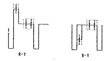
- Receive the signal of DEM pattern. Connect dual oscilloscope to Base of Q8O1 and Q8O3. Set the Color (VRIO1-3) control to maximum position. Adjust waveform to straight line with VR603, VR604 and L604.
COLOR PURITY ADJUSTMENT
The receiver must have been operating 10 minutes prior to this procedure and the face plate of the CRT must be at room temperature. The following procedure is ecommended while using a Dot/Bar Generator. 1. Check for correct location of all neck components. (Refer to Figure 1) 2. Roughtin the static components of the static
- (Refer to Figure 1) Rough-in the static convergence at the center of the CRT, as explained in the static convergence. Rotate the contrast control to maximum CCV position and rotate brightness control as far CV as possible without causing the picture to "bloom". Rotate the Red (VR801) and Blue (VR804) Cut off controls to maximum CCV position. Rotate the Green (VR803) Cut off control sufficiently in a CW direction to produce a green ractor to produce a green raster.
-
Loosen the deflection yoke clamp screw and pull the deflection yoke toward the rear of the CRI.
Begin the following adjustment with the tabs on the round purity magnet rings set together, slowly separate the two tabs while at the same time rotating them to plant for a purity for a state of the same time rotating the together. adjust for a uniform green stripe at the center of the Screen
-
- CRI screen. Carefully slide the deflection yoke forward to achieve green (uniform green screen). NOTE; Center purity is obtained by adjusting the tabs on the round purity magnet rings, outer edge purity is obtained by sliding the deflection yoke forward. Check for red and blue field purity by reducing the output of the Green (VR803) Cut off control and alternately increasing output of Red (VR801) and Blue (VR804) Cut off controls and touch up adjustments, if required. 9. Tighten deflection yoke clamp screw

Figure 1 Picture Tube Neck Component Location
BLACK AND WHITE TRACKING
The purpose of this procedure is to adjust the bias applied to the picture tube to obtain good black and white picture production at all brightness levels while, at the same time achieving maximum useable brightness. Proper RF AGC control adjustment should have been verified prior to performing this procedure.
- With antenna connected to the receiver, go to a channel with strong received. Hisadjust the fine tuning control so that the receiver will not produce a color picture while the following adjustment are being
- performed. 2. Rotate the Red (VR802) and Blue (VR805) Drive control fully CM and then back CCW to the center of their rotation ranges.
- 3. Rotate the Green (VR803), Red (VR801) and Blue (VR804) Cut off controls to the fully CCW end of their rotation
- ranges. 4. Set normal-service switch to service position. Adjust the voltage of test point (collector of green output transistor on CRI PCB) to DC140V with brightness control. Voltage measurement should be measured with an oscilloscope
- oscilloscope. 5. Rotate the screen control to the fully CCW end of its rotation range. Then, rotate it CW until a dim line of one pronounced color (green, red or blue) is obtained. 6. The other two color Cut off controls must be rotated CW until a dim white line is obtained. 7. Set normal-service switch to normal position. 8. If required, touch-up adjustment of the Red (VR802) and Blue (VR805) Drive controls to produce a uniform monochrome picture.
- 9. Rotate the brightness and contrast controls fully CCW. 10. Rotate the brightness control CW until a dim raster is
-
obtained.
11. If the screen does not display with uniformity, steps 2 through 10 of this procedure must be repeated.
-
- * (S) CRI Only --- VR803.
-
STATIC CONVERGENCE ADJUSTMENT
- 1. Switch the Receiver ON and allow it to warm up for 15 minutes. 2 Connect the output of a Crosshatch Generator to the
- minutes. Connect the output of a Crosshatch Generator to the receiver and, concentrating on the center of the CRI screen, proceed as follows: a. Locate a pair of 4 pole magnets rings. Rotate individual rings (change spacing between tabs) to converge the vertical red and blue lines. Rotate a pair of rings (maintaining spacing between tabs) to converge the horizontal red and blue lines. b. After completing red and blue center convergence, locate the pair of 6 pole magnets rings. Rotate individual rings (change spacing between tabs) to converge the vertical red and blue (magenta) and green lines. Rotate a pair of rings (maintaining spacing between tabs) to converge the vertical red and blue (magenta) and green lines.
DYNAMIC CONVERGENCE ADJUSTMENT
Dynamic convergence (convergence of the three color fields at the edges of the CRT screen) is accomplished by proper insertion and positioning of three rubber wedges between the edge of the deflection yoke and the tunnel of the CRT. This is accomplished in the following manner
- 1. Switch the Receiver ON and allow it to warm up for 15
- minutes.Apply crosshatch pattern from Dot/Bar Generator to receiver. Observe spacing between lines around edges of CRT screen.
- CKI Screen. 3. Tilt the deflection yoke up or down, and insert tilt adjustment wedges (1) and (2) between the deflection yoke and the CRT until the mis-convergence illustrated
- yoke and the CRI until the mis-convergence illustrate in Figure 2 (A) has been corrected. Tilt the deflection yoke right and left, and insert tilt adjustment wedge (3) between the deflection yoke and the CRI until the mis-convergence illustrated in Figure 2 (B) has been corrected. 4.
- rigure 2 (D) has been corrected. Alternately change spacing between, and depth of insertion of the three wedges proper dynamic
- convergence is obtained. 6. Use a strong adhesive tape to firmly secure each of the three wedges to the funnel of the CRT. 7. Check purity and adjust, if necessary.


Figure 2 Dynamic Convergence Adjustment
VIDEO LE ALIGNMENT
VIDEO IF ALTER (Refer. to Figure 3) TEST EQUIPHENT CONNECTION OSCILLOSCOPE .... Set AC-DC switch to AC position. SWEEP-MARKER GENERATOR .... Connect H SCOPE and V SCOPE output cable from SWEEP-MARKER GENERATOR to H and V input connectors on the OSCILLOSCOPE, connect hot lead of SWEEP-MARKER TOPUT cable to test point TP1 cound lead connect hot lead of SWEEP-HARKEI OUTPUT cable to test point TP1 on PCBOO1; connect ground lead to chassis ground. Connect pick up SWEEP-HARKER INPUT cable to TP7; ground lead to chassis ground.
-
Connect 10K ohm variable resistor between TP4, B+(12Y) to ground. Install AGC VR to prevent saturation in waveform, then adjust AGC VR for proper size of waveform. On the other hand, in case IF AGC voltage is supplied externally, adjust for proper size of waveform on condition that IF AGC voltage is within 10V and is gradually decreased.
Adjust L204 to obtain maximum amplitude of response curve at 38.9 HHz. (Refer to Response Curve "A")
Connect a 100 ohm resistor between TP9 and TP10. Re-connect hot lead of SWEEP-MARKER GENERATOR OUTPUT cable from TP1 to TV tuner TP.
Adjust L206 to obtain maximum amplitude of response curve.
- AUJUST L200 TO ODTAIN maximum amplitude of response curve. (Refer to Response Curve "B") Disconnect the 10K ohm variable resistor and 100 ohm resistor from the circuit.
- resistor from the circuit. Disconnect COOG. (solder bridge) Connect SWEEP-MARKER GENERATOR INPUT cable from TP7
- Connect Swill indicate oblighter in or capit from in to TPG. Adjust L203 to place 38.9 MHz marker at reference line on response curve.
- line on response curve. (Refer to Response Curve "C") Re-connect COO6. (solder bridge)

ALIGNMENT INSTRUCTIONS
SECAM CHROMA BANDPASS ALIGNMENT
SECAM CHRUMA .... (Refer to Figure 4) IEST EQUIPHENI CONNECTION GENERAL .... PAL-SECAM switch to SECAM position. SWEEP-MARKER GENERATOR ... Connect H. SCOPE and V. SCOPE output cable from SWEEP-MARKER GENERATOR to H. and V. input connectors on the OSCILLOSCOPE, connect hot lead of SWEEP-MARKER OUTPUT cable to IP on TV tuner; connect ground lead MARKER OUTPUT cable to IP on IV tuner: connect ground lead to chassis ground. Connect pick up lead SWEEP-MARKER INPUT cable to TP15; connect ground lead to TP17.
Adjust L901 to obtain best overall response curve. (Refer to Response Curve "D")
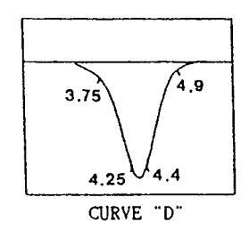


FIGURE 4
SECAM IDENT ADJUSTMENT
1.11
٥
- Receive the signal of secam color pattern. Connect the oscilloscope to TP22 and ground. Adjust the voltage to maximum with L902.
SECAM PHASE ADJUSTMENT
- Receive the signal of secam color pattern. Adjust L903 and L904 not to change the color of gound on the pattern while tuning the Color (VR101-3) control from minimum to maximum position.

DIAGRAM

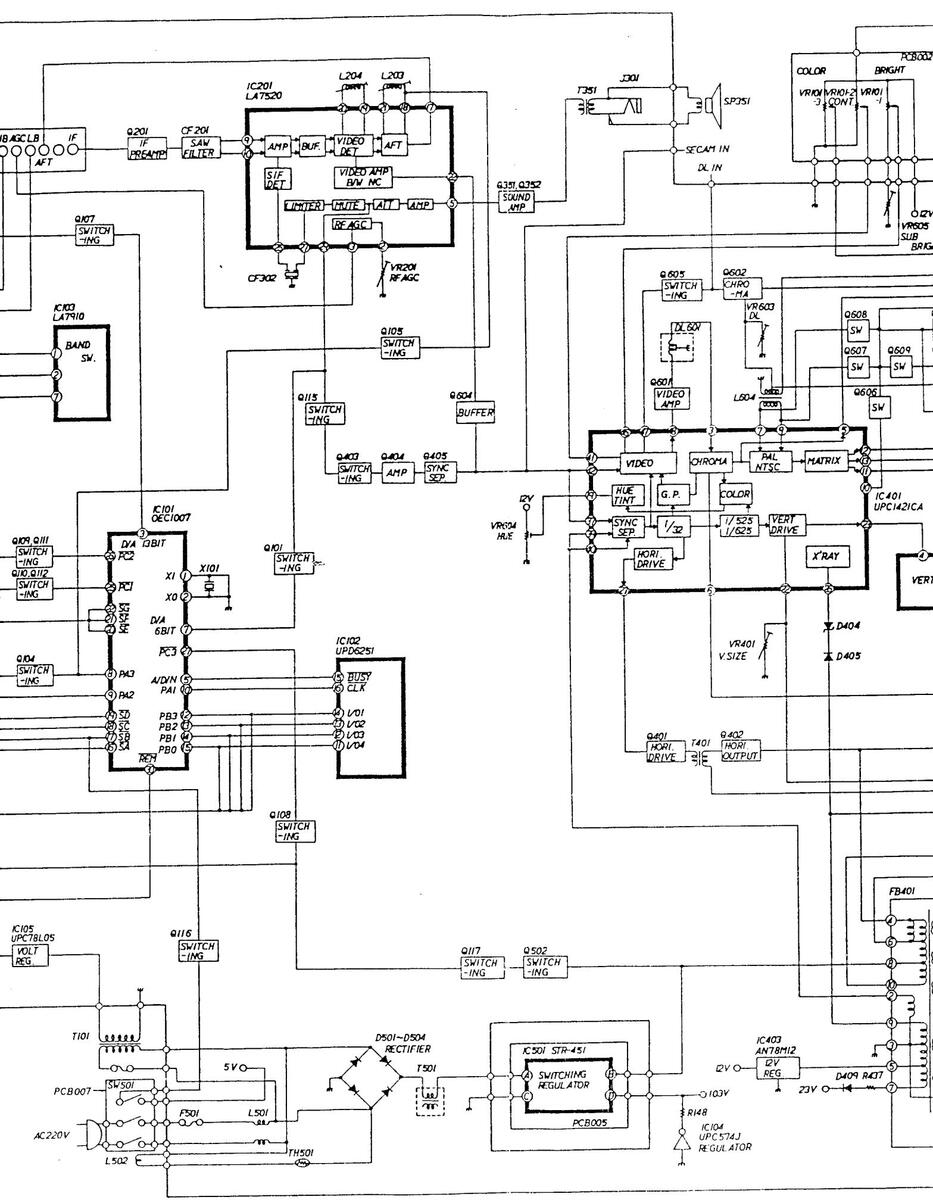
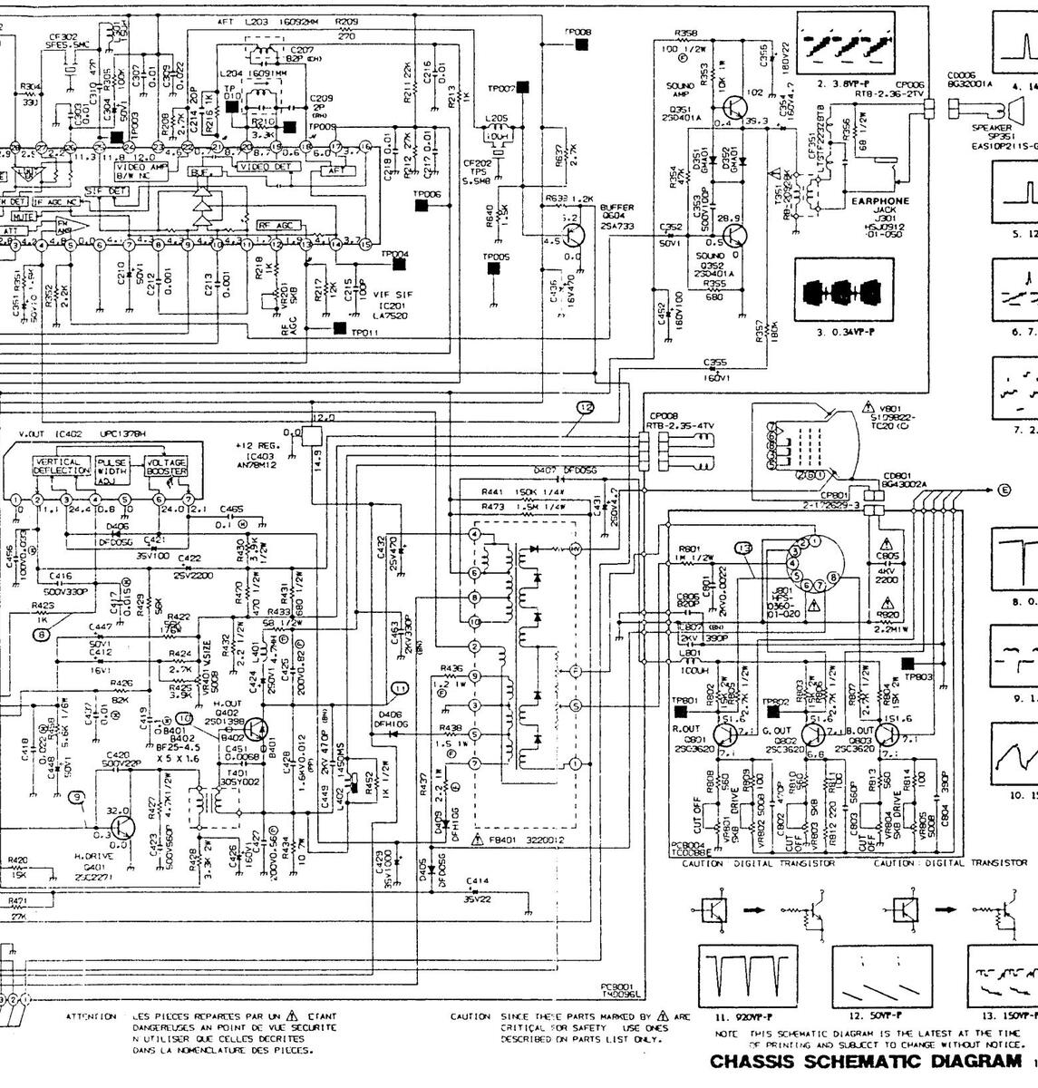
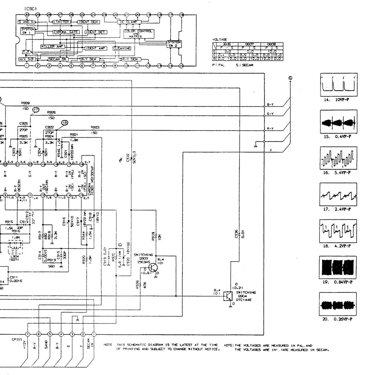
CHASSIS SCHEMATIC DIAGRAM
---------------------------------------

ASSIS SCHEMATIC DIAGRAM


CHASSIS SCHEMATIC DIAGRAM
143


143/


CHASSIS SCHEMATIC DIAGRAM

CHASSIS SCHEMAT
SCHEMATIC DIAGRAM
CHASSIS SCHEMATIC DIAGRAM
143/4


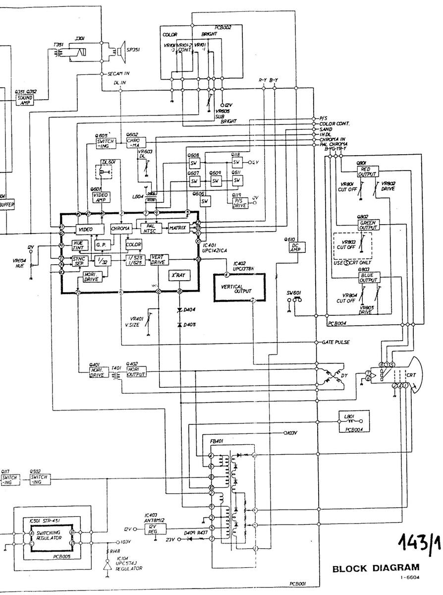
BLOCK DIAGRAM
3-2325

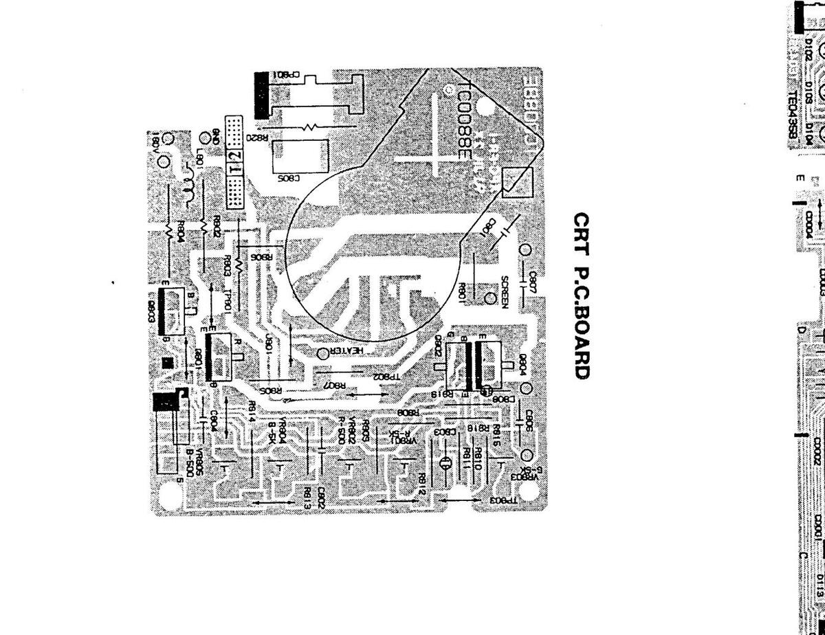
MAIN P.C.BOARD

MAIN P.C.BOARD


SECAM P.C.BOARD

CONTROL P.C.BOARD

SECAM P.C.BOARD

ĩ

РОМЕВ Р.С.ВОАВD

M P.C.BOARD


MECHANICAL REPLACEMENT PARTS LIST
REE NO PART NO DESCRIPTION ADEAETATOD CARINET FRONT ASS'Y 43343/4/23 CABIN 7138900016 0000 TISKPUOUIS DOOR (3/KPA0013 BUTTON, CAP 735KPA0027 BUTTON, CHANN 00+20#T13 ISONFAULUS BUILUNIE BUUKFUUUAI FU SHEET CABINET , BAC. SHEET PATING SHEET, RAIING 751 JNA0004 PLATE FARTH WLRF 751 JNA0004 PLATE EARTH WIRE TAIKUANNOS SPRING FARTH TELEBADOSS EDANE OF 761KSA0062 FRAME, CRI 800KR00002 SHEET, CRT SUPPORT 749KUA0002 SPRING, ANTENNA 8407630604 TAP TITE(S) BRAZIER 3*6 CH 4#20 01 BAUISSUBUS IAP IIICSI ANTEADARD TAPPING (D) TOUS 4419 00 4*18 BK 6.3*22*T1.6 SOALISHUMOL TAREER 46 ADDEEDODA SI NU 204 8300560004 SL NUT 9015080000 EARTH LUG(E8) JIAKTGADZA GUARANTEE CARD JIANIGAUZA GUARANTEE CARD JIAKINFULE INSTRUCTION JIAKIKFUOF FID SHEET JIAKTKI03G SCHEMATI 791KHA0011 POLT BAG 791KHA0014 POLY BAG 791KHA0033 SHEET,LIGHTRON TSIKHADOSA PACKAGE.TOP 192KHAUUS4 PACKAGE, 107 792KHA0055 PACKAGE, BOTTON 793KCD0763 GIFT BOX
THIS ELECTRICAL PARTS LIST IS A STANDARD PART LIST, BUT INTERCHANGEABLE PARTS MAY BE USED IN THE UNIT. SEE THE INTERCHANGEABLE PARTS LIST AFTER THE STANDARD PARTS LIST.
ELECTRICAL REPLACEMENT PARTS LIST
| REF.NO | PART . NO | DESCRIPTI | ON | REF.NO | PART . NO | DESCRIPTIO | ON | |
|---|---|---|---|---|---|---|---|---|
| -RESISTORS- | * | -SEMICONDUCTORS | (CONT)- | |||||
|
R002
R148 R158 R353 R358 R413 R428 R433 R434 R434 R436 |
R615846R8J
R31181123J R61584181J R31181103J R61582101J R31181123J R3118A332J R51582680J R55M2CE100J R614811R2J |
R.FUSE
R.METAL OXIDE R.FUSE R.METAL OXIDE R.FUSE R.METAL OXIDE R.METAL OXIDE R.FUSE R.CEMENT R.FUSE |
6.8 OHM 1/4W
12K OHM 1 W 180 OHM 1/4W 10K OHM 1 W 100 OHM 1/2W 12K OHM 1 W 3.3K OHM 2 W 68 OHM 1/2W 10 OHM 7 W 1.2 OHM 1 W |
D127
D128 D129 D130 D136 D139 D140 D351 D352 D401 |
D25T5566B0
D13TDS442X D25T5566B0 D13TDS442X D13TDS442X D13TDS442X D13TDS442X D13TGMA010 D13TGMA010 D13TGMA010 |
DIODE, RECTIFIER
DIODE, SILICON DIODE, RECTIFIER DIODE, RECTIFIER DIODE, SILICON DIODE, SILICON DIODE, SILICON DIODE, SILICON DIODE, SILICON DIODE, SILICON |
S5566B
DS442X-BT S5566B S5566B DS442X-BT DS442X-BT DS442X-BT GMA-01-BT GMA-01-BT GMA-01-BT |
|
|
R437
R438 R501 R506 R509 R661 R665 R665 R666 R671 R802 |
R615812R2J
R615811R5J R5M2CD5R6K R3118A220J R31181103J R0D104102J R0D104822J R0D108392J R0D104473J R3118A153J |
R,FUSE
R,FUSE R,CEMENT R.METAL OXIDE R,METAL OXIDE RC RC RC RC R,METAL OXIDE |
2.2 OHM 1 W
1.5 OHM 1 W 5.6 OHM 5 W 22 OHM 2 W 1.0K OHM 1 W 1.0K OHM 1/4W 3.9K OHM 1/4W 47K OHM 1/4W 15K OHM 2 W |
D402
D403 D404 D405 D406 D407 D408 D409 D409 D411 D416 |
D13TGMA010
D13TGMA010 D93T01100Y D23TFD05TG D23TFD05TG D23TFD05TG D23FFH10TG D13TGMA010 D13TGMA010 |
DIODE, SILICON
DIODE, SILICON DIODE, ZENER DIODE, RECTIFIER DIODE, RECTIFIER DIODE, RECTIFIER DIODE, RECTIFIER DIODE, RECTIFIER DIODE, SILICON |
GMA-01-BT
GMA-01-BT GZA11 Y BT DFD05TG-BT DFD05TG-BT DFD05TG-BT DFH10TG-KB4 OFH10TG-KB4 GMA-01-BT GMA-01 |
|
| ₫ |
R803
R804 R820 R922 |
R3118A153J
R3118A153J R03101225J R615846R8J |
R.METAL OXIDE
R.METAL OXIDE RC R.FUSE |
15K OHM 2 W A
15K OHM 2 W A 2.2M OHM 1 W A 6.8 OHM 1/4W A |
D501
D502 D503 D504 D505 |
D28020E100
D28020E100 D28020E100 D28020E100 D28020E100 D28F00RU20 |
DIODE, SILICON
DIODE, SILICON DIODE, SILICON DIODE, SILICON DIODE, SILICON |
20E10
20E10 20E10 20E10 20E10 |
|
C008
C214 C356 C403 |
C0B0F04H4Z
C0B0SL421K E025FB220M C0B0B0514K |
-CAPACITORS-
CC CC CC CC CC |
0.022 UF 50V ZF
20 PF 50V UK 22 UF 160V 10000 PF 50V B |
D506
D507 D508 D602 D603 |
D2B000RH10
D2B000RH10 D2B000R2M0 D13TGMA010 D13TGMA010 |
DIODE, RECTIFIER
DIODE, RECTIFIER DIODE, AVARANCHE DIODE, SILICON DIODE, SILICON |
RH-1
RH-1 R2M GMA-01-BT GMA-01-BT |
|
|
C422
C425 C427 C428 C429 C429 C431 |
E087F3222M
P441F2824J P441F2564J P442F9123J E08704102M E085FD4R7M |
CE
CMPP CMPP CMPP CE CE CE |
2200 UF 25V
0.82 UF 200V 0.56 UF 200V 0.012 UF1600V 1000 UF 35V 4.7 UF 250V |
D604
D605 D606 D607 D613 |
D13TGMA010
D13TDS442X D13TGMA010 D13TGMA010 D13TGMA010 |
DIODE, SILICON
DIODE, SILICON DIODE, SILICON DIODE, SILICON DIODE, SILICON |
GMA-01~BT
DS442X-BT GMA-01-BT GMA-01-BT GMA-01-BT GMA-01-BT |
|
| ▲ |
C449
C452 C463 C502 C503 C508 C509 C511 C513 C515 |
C01BBN7G2K
E025FB101M C03BBN7L2K E0260H101T P442F9332J C02FB07H3K C02FB07H3K C02FB07H3K P4440B474M C03BBN7W2K |
CC
CE CC CC CC CC CC CC CC CC CC CC CC C |
0.00047UF 2KV B
100 UF 160V 330 PF 2KV 100 UF 400V 0.0033UF 1600V 0.0022UF 2KV B 0.0022UF 2KV B 0.0022UF 2KV B 0.47 UF 250V Δ 820 PF 2KV BN |
| C101
| C102 | C103 | C104 | C105 | C201 | C401 | C402 | C403 | C501 |
I 52D010070
I 320062510 I 03S079100 I 02190574J I 02A98L050 I 03DE75200 I 02DE1421A I 02SD13780 I 01A98M120 I 2B3904510 |
OEC1007
UPD6251C LA7910 UPC574J-T UPC78L05 LA7520 UPC1421CA UPC1378H AN78M12 STR-451 |
|
| C516 | CO3BBN7N2K | cc | 390 PF 2KV BN | 10901 | 106DC13970 | IC | M51397AP | |
| ۵ |
C518
C519 C611 C801 C805 C807 |
C01BBN713K
C03BBN7W2K C0B0F0414Z C02FB07H3K C030E09H3M C03BBN7N2K |
CC
CC CC CC CC CC CC CC CC CC CC CC CC |
0.001 UF 2KV BN
820 P 2KV BN 0.01 UF 50V ZF 0.0022UF 2KV B 2200 PF 4KV E 390 PF 2KV BN SL-1263H |
Q101
Q104 Q105 Q106 Q107 Q108 Q109 Q110 Q111 Q112 |
TP7TB03001
TN7TG03001 TC2T009450 TN7TG03001 TC2T009450 TN7TB03001 TA2T009520 TA2T009520 TN7TF03001 TN7TF03001 |
COMPOUND TRANSISTOR
COMPOUND TRANSISTOR TRANSISTOR.SILICON COMPOUND TRANSISTOR TRANSISTOR.SILICON COMPOUND TRANSISTOR TRANSISTOR.SILICON TRANSISTOR.SILICON COMPOUND TRANSISTOR COMPOUND TRANSISTOR |
DTA114E S-T
DTC124X S-T 2SC945-T DTC124X S-T 2SC945-T DTC114E S-T 2SA952-T 2SA952-T DTC114Y S-T DTC114Y S-T |
|
D102
D103 D104 D105 D106 D107 D108 D109 D110 D111 |
0021321020
0021321020 0021321020 0021321070 0021321070 0021321070 0021321070 0131DS442X D13TDS442X |
LED
LED LED LED LED LED DIODE,SILICON DIODE,SILICON |
SLP-136B
SLP-136B SLP-136B-50 SLP-136B-50 SLP-136B-50 SLP-136B-50 DS442X-BT DS442X-BT |
Q115
Q116 Q117 Q118 Q119 Q201 Q351 Q351 Q352 Q401 Q402 |
TC2T009450
TC2T009450 TC3T029095 TC2T009450 TC3T030000 TC3T030000 TD200401A0 TC3T022710 TC3T022710 TC3T022710 |
TRANSISTOR.SILICON
TRANSISTOR.SILICON TRANSISTOR.SILICON TRANSISTOR.SILICON TRANSISTOR.SILICON TRANSISTOR.SILICON TRANSISTOR.SILICON TRANSISTOR.SILICON TRANSISTOR.SILICON TRANSISTOR.SILICON |
2SC945-T
2SC945-T 2SC2909S 2SC945-T 2SC3000-AA 2SD401A 2SD401A 2SC2271-AE |
|
|
D112
D113 D114 D115 D116 D116 D118 D119 D120 D121 D122 |
D13TGMA010
D13TGMA010 D13TGMA010 D13TGMA010 D13TDS442X D13TDS442X D13TDS442X D13TDS442X D13TDS442X D13TDS442X D13TGMA010 |
DIODE, SILICON
DIODE, SILICON DIODE, SILICON DIODE, SILICON DIODE, SILICON DIODE, SILICON DIODE, SILICON DIODE, SILICON DIODE, SILICON DIODE, SILICON |
GMA-01-BT
GMA-01-BT GMA-01-BT DS442X-BT DS442X-BT DS442X-BT DS442X-BT DS442X-BT GMA-01-BT DS442X-BT |
0403
0404 0405 0502 0601 0602 0604 0605 0606 0607 |
TC2T009450
TC2T009450 TA2T007330 TB3T00698E TA2T007330 TA2T007330 TA2T007330 TC2T009450 TC2T009450 |
TRANSISTOR, SILICON
TRANSISTOR, SILICON TRANSISTOR, SILICON TRANSISTOR, SILICON TRANSISTOR, SILICON TRANSISTOR, SILICON TRANSISTOR, SILICON TRANSISTOR, SILICON TRANSISTOR, SILICON |
2SC1398-Y80
2SC945QT 2SC945QT 2SB698E-AA 2SA733QT 2SA733QT 2SA733QT 2SC945-T 2SC945-T 2SC945QT |
|
|
D123
D125 D126 |
D13TGMA010
D13TGMA010 D13TDS442X |
DIODE, SILICON
DIODE, SILICON DIODE, SILICON |
GMA-01-BT
GMA-01-BT DS442X-BT |
Q608
Q609 Q610 Q611 Q801 Q802 Q803 Q903 |
TN7TD03001
TC2T009450 TC2T009450 TN7TD03001 TC5F03620S TC5F03620S TC5F03620S TC5F03620S TC5F03620S |
COMPOUND TRANSISTOR
TRANSISTOR.SILICON TRANSISTOR.SILICON COMPOUND TRANSISTOR TRANSISTOR.SILICON TRANSISTOR.SILICON TRANSISTOR.SILICON TRANSISTOR.SILICON |
DTC144E S-1
DTC144E S-1 2SC9450T 2SC945-T DTC144E S-1 2SC3620(LB) 2SC3620(LB) 2SC3620(LB) 2SC3620(LB) 2SC3620(LB) |
| REF.N | PART.NO | DESCRIPT | ION | REE M | ||||||
|---|---|---|---|---|---|---|---|---|---|---|
| -SEMICONDUCTORS (CONT)- | NEF.NC | PART.NO | DESCRIPTION | |||||||
| Q904 INTTD03001 COMPOUND TRANSISTOR DIGINAL C | -MISCELLANEOUS ( | -MISCELLANEOUS (CONT)- | ||||||||
|
Q905
L202 L203 L204 |
TN7TD03001
021673R82N 033602002F 033500005F |
COMPOUND TRANSISTO
-COILS & TRANSF COIL ELOGOGRA-R82M COIL VIDEO IFT COIL VIDEO IFT |
R DTC144E S-T
R DTC144E S-T DTC144E S-T DRMERS- 0.82 UH 16092MM 16091MM 10 UH 16084SU 15 UH 4.7 MH 1450MS 91000002 8X200008 |
۸ |
CD005
CD006 CD007 CD008 CD010 CD101 CD102 |
1224041402
0686320014 1224051501 1224031501 1224031501 0694290030 0694260040 120L451003 068612183A 068601173A |
CORD.JUMPER
CORD.EIS CONNECTOR CORD.JUMPER CORD.JUMPER CORD.JUMPER CONNECTOR PCB SIDE CONNECTOR PCB SIDE CORD.AC CORD.JUMPER CORD.CONNECTOR |
24041402
8G32001A 24061501 24031501 24031101 174074-9 8FEET 8G12183A 8G01173A |
||
|
L205
L206 L301 L401 |
021673100K
033500001G 021673150K 021679472K |
COIL ELOGOGRA-100K
COIL,VIDEO IFT COIL ELOGOGRA-150K COIL ELOGOGRA-150K |
CD501
CD502 CD503 CD504 |
|||||||
| £ |
L501
L502 L602 |
0221000004
0291000002 028Y200008 021673470K |
COIL,LINEARITY
COIL,LINE FILTER COIL,DEGAUSS |
CD801
CD802 CF001 CF002 |
068G43002A
122N055305 116F3TH4Z1 116F3TH4Z1 |
CORD.CONNECTOR
CORD.JUX CONNECTOR FILTER.EMI FILTER.EMI FILTER.EMI FILTER.EMI FILTER.SAW FILTER.SAW FILTER.CERAMIC TRAP FILTER.CERAMIC |
8G01174A
8G43002A 2N055305 LTSTF2232BTB LTSTF2232BTB LTSTF2232BTB LTSTF2232BTB F1034 TPS5.5MB CDA5.5MC24B |
|||
|
L603
L604 L606 L801 L901 L902 |
021673586K
0335000096 021673470K 021JA2101K 03302R0016 03352R0106 |
COIL ELOGOGRA-5R6K
COIL,MATCHING COIL ELOGOGRA-470K COIL LALO3TA101K COIL,CHROMA COIL,CHROMA |
47 UH
5.6 UH 3500009 47 UH 100 UH 16032SU 3532010 |
CF003
CF004 CF201 CF202 CF301 |
116F3TH4Z1
116F3TH4Z1 1027038R91 1012105R51 101225R501 |
|||||
|
L903
L904 L905 |
03352R006G
03352R006G 021JA6470K |
COIL, CHROMA
COIL, CHROMA COIL, LAL02TA470K |
16071
16071 47 UH |
CF 302
CF 351 CP006 CP008 |
1012005R52
116F3TH4Z1 069Z320018 069Z420039 0694FC0010 0694290040 0694260050 069RFA0040 069RF70040 |
FILTER, CERAMIC
FILTER, EMI CONNECTOR PCB SIDE CONNECTOR PCB SIDE CONNECTOR PCB SIDE F-CHIP CONNECTOR PCB SIDE CONNECTOR PCB SIDE CONNECTOR PIN CONNECTOR PIN |
SFE5.5MC
LTSTF223ZBTB RTB-2.36-2TV RTB-2.36-4TV 069Z420039 1-163740-1 174161-9 174161-6 5530-108 5530-078 |
|||
| L907 | 0216738R2K | COIL EL0606RA-8R2K | 8.2 UH |
CP009
CP012 |
||||||
| * |
T101
T351 T401 T501 |
040511008E
045284001K 03305Y002G 0481330015 |
TRANSFORMER POWER /
TRANSFORMER,SOUND ( TRANS,HORIZONTAL DE TRANSFORMER,SWITCH |
C 0511008
NUTPUT RB-20928K NVE 305Y002 NG RB-20855 |
CP102
CP110 CP111 |
|||||
| -JACKS- |
CP505
CP801 |
0695010049
0694430100 |
CONNECTOR PCB SIDE CONNECTOR |
WP22-1(W)
2-172629-3 |
||||||
| ۵ |
J301
J801 |
0602101004
0662130007 |
JACK, RCA 3.5
SOCKET, CRT -SWITCHES- |
HSJ0912-01-050
HPS0360-01-020 |
CP802
CP803 DL601 DL901 EAB351 |
0675105019
0675105019 103100601 104114R43G 074J130001 0808T2R502 0432200121 067H000003 |
WIRE HOLDER
WIRE HOLDER DELAY DELAY LINE GLASS EARPHONE FUSE TRANSFORMER,FLYBACK HOLDER,FUSE |
WH5D-1
WH5D-1 ELT-102246N EFDEN645A31F 3.5FA1.3M.16 OHM EAK2.5 A(T) 250 3220012 773JEE0004 |
||
|
SW101
SW102 SW103 SW104 SW105 |
0504211004
0504211004 0504211004 0504211004 0504211004 |
SWITCH, PUSH
SWITCH, TACT SWITCH, TACT SWITCH, TACT SWITCH, TACT |
SPPH11280A
SKHHAN012A SKHHAN012A SKHHAN012A |
F501
FB401 FH501 |
||||||
|
SW106
SW107 SW108 SW109 SW110 |
0504211004
0504211004 0504211004 0504211004 0504211004 |
SWITCH, TACT
SWITCH, TACT SWITCH, TACT SWITCH, TACT SWITCH, TACT SWITCH, TACT |
SKHHANO12A
SKHHANO12A SKHHANO12A SKHHANO12A SKHHANO12A SKHHANO12A |
FH502
MS001 MS002 NR101 NR102 OS101 |
067H000003
128F000003 128B000016 110E447301 110E747301 077M006004 |
HOLDER,FUSE
MICA,SHEET MICA,SHEET R.NETWORK R.NETWORK REMOTE RECEIVER SPACER SPACER SPEAKER DEGAUSS ELEMENT |
773JEE0004
1S-3MPC TO-3(5) RN3H5A473J01A RN3H8A473J01A KEY-C00SV2 BUSH-T EAS-10P211SG ERP-F5B0M180H |
|||
| ♪ |
SW111
SW112 SW501 SW601 |
0504211004
0504211004 0530102008 0510422001 |
SWITCH,TACT
SWITCH,TACT SWITCH,PUSH SWITCH,SLIDE |
SKHHANO12A
SKHHANO12A ESB-76937A SS-009-7H |
S002
SP351 TH501 |
128F100005
128F100005 070G043001 D810M180H0 |
||||
| -VARIABLE RESISTORS- | 4 | TM101 C | 0766092009 |
TRANSMITTER
TUNER, UHE-VHE |
EUR-53724 | |||||
|
VR101
VR201 VR401 VR603 VR604 VR605 VR801 VR802 VR803 VR803 VR804 |
V029300007
V115353802 V115352802 V126302801 V126304801 V126304801 V175C53801 V175C52801 V175C53802 V175C53803 |
VR.ROTARY RK09
VR.SEMIFIXED EVN- VR.SEMIFIXED RHEO VR.SEMIFIXED RHEO VR.SEMIFIXED RHEO VR.SEMIFIXED RHEO VR.SEMIFIXED RVAO VR.SEMIFIXED RVAO VR.SEMIFIXED RVAO VR.SEMIFIXED RVAO |
Z3330012
52JA00853 52JA00852 AS20FB(H0615C105) A140FB(H0615C113) AS40CA(H0615C117) 911H304-1-502M 911H304-1-502M 911H304-2-502M 911H304-3-502M |
V801
X101 X401 X601 |
098F200410
10024R5002 1002R50002 100H4R4306 |
TUBE/CATHODE RAY
CERAMIC/OSCILLATOR CERAMIC/OSCILLATOR CRYSTAL HC49 |
EC-CB-0309
5109B22-TC20(C) CSA4.50MG CSB500F2 //U 4.433619MHZ |
|||
| VR805 | V175C52B03 | VR.SEMIFIXED RVAD | 911H304-3-501M | |||||||
| -P.C. BOARDS ASS'Y- | ||||||||||
|
PCB001
PCB002 PCB003 PCB004 PCB005 PCB006 PCB007 |
A35457A010S
A35457A030 A35457A200 A35457A110 A35457A020 A35457A140 A35457A380 |
PCB ASS'Y
PCB ASS'Y PCB ASS'Y PCB ASS'Y PCB ASS'Y PCB ASS'Y PCB ASS'Y |
TM0096L-S
TE0435B TE0435B TC0088E TE0156A TE0299H TE0299H TE03574 |
RESIST
RC |
RESISTOR
RCCARBON RESISTOR CAPACITORS |
|||||
| -MISCELLANEOUS- | CE | CERAMI |
C CAPACITOR
ELECTROLYTIC CAPACIT |
OR | ||||||
| ▲ |
ANT001
B401 B402 BT101 BT102 CD001 CD002 CD003 CD004 |
0637300001
0246451652 0246451652 141T004003 141T004003 1224051201 1224051202 1224041202 |
ATC UNIT
CORE, BEADS CORE, BEADS BATTERY, MANGAN BATTERY, MANGAN CORD, JUMPER CORD, JUMPER CORD, JUMPER CORD, JUMPER |
ATCU-PS-K
BF25-4.5*5*1.6 BF25-4.5*5*1.6 UM-4 UM-4 24051201 24051201 24051202 24041204 24041202 |
CPPOLYESTER CAPACITOR
CPPPOLYESTER CAPACITOR CPDPLASTIC CAPACITOR CMPMETAL POLYESTER CAPACITOR CMPLMETAL PLASTIC CAPACITOR CMPPMETAL POLYPROPYLENE CAPACITOR CMPPMETAL POLYPROPYLENE CAPACITOR CSTSTYROL CAPACITOR |
TOR | ||||
S-T LB)OR
ÀA
АЕ УВС
AA
17
INTERCHANGEABLE PARTS LIST
NOTE: THE FOLLOWING PART(S) MAY BE SUBSTITUTED FOR PARTS INDICATED IN THE BASIC PART(S) LIST (WITH THE SAME REF.NO.). THESE PARTS SHARE THE SAME ELECTRICAL CHARACTERISTICS AND OTHER ELEMENTS FOR COMMON USAGE. EITHER PART NUMBER MAY BE USED IN THIS UNIT.
| REF.NO. |
DESCRIPTION
(PART NO.) |
DESCRIPTION
(PART NO.) |
|---|---|---|
| T501 | RB-20855 | 8133010T |
| SW601 | SS-009-7H |
(048133010T)
SS-22F1607 |
| CD501 |
(0510422001)
8FEET |
(0510B22001)
120S451003 |
| X601 |
(120L451003)
HC49/U 4.433619MHZ |
(1205451003)
HC-49/U 4433.619KH |
|
(100H4R4306)
# |
(10064R4306) |
•


 Loading...