

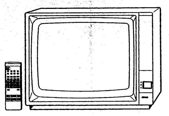
ORION COLOR TELEVISION RECEIVER

COLOR 514 Hanseatic C 1555 VT
Bei technischen Änderungen können Ergänzungsblätter angefordert werden.
Specifications are subject to change without notice.
CHASSIS CODE D

PAL/SECAM
SPECIFICATIONS
| PICTURE SIZE |
20 inch
PAL/SECAM |
|---|---|
| FREQUENCY RANGE VHF(L) | 2 - 4, X - S2 ch |
| S3 - S10, 5 - 12, S11 - S20 ch | |
| MAXIMUM SENSITIVITY VHF | 20 dB |
| UHF | 25 dB |
| Picture IF Carrier Frequency | 38.9 MHz |
| Color Sub Carrier Frequency | 34.47 MHz |
| SOUND INTERMEDIATE FREQUENCY |
33.4 mHz
5.5 MHz |
| MAXIMUM OUTPUT POWER | 2.0 W |
| POWER SOURCE | AC 220V |
- IMPORTANT
*FOR SERVICE WORK ALWAYS USE MAINS ISOLATING TRANSFORMER, CHASSIS IS LIVE. (IRRESPECTIVE OF POLARITY OF MAINS PLUG.)
*IN CASE OF REMOVING PCB OR SOMETHING, AFTER UNFASTENING THE WIRE OR CHANGING THE WIRE POSITION, IT IS IMPORTANT TO PUT THE FASTENING OF WIRE AND THE POSITION OF WIRE AS IT WAS. BECAUSE, PICTURE DISTORTION OR SOMETHING MAY APPEAR ON THE DISPLAY. SO, BE SURE TO CONFIRM THE FASTENING AND POSITION OF WIRE BEFOREHAND. THEN START TO THE OPERATION.
*INFERIOR SILICON GREASE CAN DAMAGE IC'S AND TRANSISTORS. WHEN REPLACING AN IC OR TRANSISTOR, USE ONLY SPECIFIED SILICON GREASE (YG6260). REMOVE ALL THE OLD SILICON BEFORE APPLYING NEW SILICON.
CONTENTS
| FAGE | |
|---|---|
| SPECIFICATIONS | 1 |
| ALIGNMENT INSTRUCTIONS | 2~4 |
| MAJOR COMPONENTS LOCATION GUIDE | 5 |
| BLOCK DIAGRAMS | 6 |
| MAIN P.C.BOARDS | 7 |
| CONTROL/LED/CRT/T TEXT/POWER SWITCH P.C.BORDS | 8 |
| MAIN/CONTROL SCHEMATIC DIAGRAMS | 9 |
| MAIN SCHEMATIC DIAGRAMS | 10 |
| MAIN/POWER/CRT SCHEMATIC DIAGRAMS | 11 |
| T'TEXT SCHEMATIC DIAGRAMS | 12 |
| MECHANICAL EXPLODED VIEW | 13 |
| MECHANICAL REPLACEMENT PARTS LIST | 14 |
| ELECTRICAL REPLACEMENT PARTS LIST | 15~16 |
| INTERCHANGEABLE PARTS LIST | 17 |
SHUT DOWN CIRCUIT
When the high voltage rises, a simultaneous voltage increase will develop at terminal 9 of the Horizontal Output Iransformer(FB401), and be applied to pin 52 of IC401. If excessive high voltage is produced, the increased voltage developed exceeds the rating of zener diode D405 causing the Horizontal Oscillator to stop functioning and the high voltage system to shut down.
HORIZONTAL AND VERTICAL SIZE ADJUSTMENT
Adjust the control (VR501) and (VR401) so that the picture fills the picture from top to bottom and is proportionate to the width.
RF AGC ADJUSTMENT
The RF AGC control is adjusted at the factory and rarely requires re-adjustment unless the received picture exhibits too much snow or the receiver lacks sensitivity. Home adjustment can be made by tuning in a weak snowy station and adjusting RF AGC for the least amount of snow. For a more accurate adjustment, use the following procedure
Receive the test pattern signal (80dB). Adjust AGC pin of IV tuner (IP011) to 4.75V with VR201 control
SUB BRIGHT ADJUSTMENT
- Receive the Monochrome Pattern. Press the NORMAL button on the remote control unit Adjust VR603 until 0% of gray scale will be black.
FOCUS ADJUSTMENT
Adjust focus control on the flyback transformer for a defined picture.
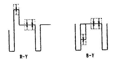
HUE DELAY ADJUSTMENT
- . Receive the DEM Pattern.
- A. Adjust waveform to straight line with VR601 and L603.
VERTICAL POSITION ADJUSTMENT
- Receive the Color Bar Pattern.
- Adjust $W401 until the horizontal line of the color bar will come to around center of the CRI.
HORIZONTAL POSITION ADJUSTMENT
- . Receive the Color Bar Pattern.
- Receive the color bar rattern. Adjust VR402 until the color width of both ro screen edges will be equal. Receive broadcasting signal, than confirm picture
- is normal.
SUB COLOR ADJUSTMENT
- . Receive the Color Bar Pattern. . Press the NORMAL button on the re . Connect the oscilloscope to IP801 emote control unit.
- J. Connect the oscilloscope to IP801. Adjust VR602 until red color level will be 75%
T'TEXT FREQUENCY ADJUSTMENT
- Receive the noise signal. Connect the frequency counter to IP851. Adjust TC851 until the counter will be 6.001 MHz.
COLOR PURITY ADJUSTMENT
CW 7. Set 8. If (VR
uni Rot Rot 9. 10.
obt 11
STATI
. Sw: mi: 2. Co:
re
ço pa Af 1c
DYNA Dynam at the
inser the e
Thie
. Su 2. Ap re CR Ii ad
yc 11
81 ir 5. Al
₿6. Ŭ 1 7. Ci
2.
-
COLUR PURITY ADJUSIMENT
The receiver must be operated 10 minutes prior to this procedure and the face plate of the CRI must be at room temperature. The following procedure is recommended while using a Dot/Bar Generator.
1. Check for correct location of all neck components. (Refer to Fig. 1)
2. Rough-in the static convergence at the center of the CRI, as explained in the static convergence.
3. Rotate the contrast control to maximum CCW position and rotate brightness control as far CW as possible without causing the picture to "bloom".
4. Rotate the Red (VR801) and Blue (VR804) Cut off controls to maximum CCW position. Rotate the Green (VR803) Cut off control sufficiently in a CM direction
5. Loosen the deflection yoke clamp screw and pull the deflection yoke toward the rear of the CRI.
6. Begin the following adjustment with the tabs on the round purity magnet rings set together, slowly separate the two tabs while at the same time rotating them to adjust for a uniform green stripe at the center of the adjust for a uniform green stripe at the center of the CRI screen.
- CRT screen. 7. Carefully slide the deflection yoke forward to achieve green (uniform green screen). NOIE: Center purity is obtained by adjusting the tabs on the round purity magnet rings, outer edge purity is obtained by sliding the deflection yoke forward.
- yoke forward. 8. Check for red and blue field purity by reducing the output of the Green (VR803) Cut off control and alternately increasing output of Red (VR801) and Blue (VR804) Cut off controls and touch-up adjustments, if required. 9. Lighten deflection yoke with clamp screw.
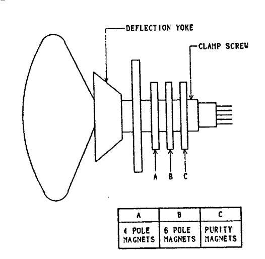
Fig. 1 Picture Tube Neck Component Location
BLACK AND WHITE TRACKING
The purpose of this procedure is to adjust the bias applied to the picture tube to obtain good black and white picture production at all brightness levels while, at the same time achieving maximum useable brightness. Proper RF AGC control adjustment should have been verified prior to performing this procedure.
- rorming this procedure. With antenna connected to the receiver, go to a channel with strong reception. Adjust the fine tuning control so that the receiver will not produce a color picture while the following adjustment are being
- Rotate the Red (VR802) and Blue (VR805) Drive control fully CW and then back CCW to the center of their
- rotation ranges. 3. Rotate the Green (VR803), Red (VR801) and Blue (VR804) Cut off controls to the fully CCW end of their rotation ranges. 4 Set nor
- ranges. Set normal-service switch to service position. Adjust the voltage of test point (collector of green output transistor on CRI PCB) to DCI50V with sub brightness control. Voltage measurement should be measured with an
- oscilloscope. 5. Rotate the screen control to the fully CCW end of its rotation range. Then, rotate it CW until a dim line of one pronounced color (green, red or blue) is obtained.
- The other two color Cut off controls must be rotated CW until a dim white line is obtained. Set normal-service switch to normal position. If required, perform touch-up adjustment of the Red (VR802) and Blue (VR805) Drive controls to produce a uniform monochrome picture. Rotate the brightness and contrast controls fully CCW. Rotate the brightness control CW until a dim raster is obtained
- obtained.
- If the screen does not display with uniformity, steps 2 through 10 of this procedure must be repeated.
STATIC CONVERGENCE ADJUSTMENT
at Ided
n and thout
.1 Stion ne
he parate to E the
ieve tabs
ze on
ine of
ained
- 1. Switch the Receiver ON and allow it to warm up for 15
- minutes. Connect the output of a Crosshatch Generator to the receiver and concentrating on the center of the CRI screen, proceed as follows:
- screen, proceed as follows: Locate a pair of 4 pole magnet rings. Rotate individual rings (change spacing between tabs) to converge the vertical red and blue lines. Rotate a pair of rings (maintaining spacing between tabs) to converge the horizontal red and blue lines. After completing red and blue center convergence, locate a pair of 6 pole magnet rings. Rotate individual rings (change spacing between tabs) to converge the vertical red and blue (magenta) and green lines. Rotate a pair of rings (maintaining spacing between tabs) to converge the horizontal red and blue (magenta) and green lines.
DYNAMIC CONVERGENCE ADJUSTMENT
Dynamic convergence (convergence of the three color fields at the edges of the CRI screen) is accomplished by proper insertion and positioning of three rubber wedges between the edge of the deflection yoke and the tunnel of the CRI. This is accomplished in the following manner.
- 1. Switch the Receiver ON and allow it to warm up for 15 minutes.
- manutes. Apply crosshatch pattern from Dot/Bar Generator to receiver. Observe spacing between lines around edges of CRI screen.
-
CRI screen.
3. Tilt the deflection yoke up or down, and insert tilt adjustment wedges (1) and (2) between the deflection yoke and the CRI until the improper convergence illustrated in Fig. 2 (A) has been corrected.
4. Tilt the deflection yoke right and left, and insert tilt adjustment wedge (3) between the deflection yoke and the CRI until the improper convergence illustrated in Fig. 2 (B) has been corrected.
5. Alternately change spacing between, and depth of insertion of the three wedges proper dynamic convergence is obtained.
- convergence is obtained.
-
6. Use a strong adhesive tape to firmly secure each of the three wedges to the funnel of the CRI.
7. Check purity and adjust, if necessary.
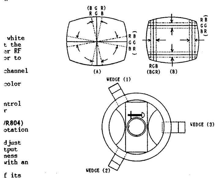
Fig. 2 Dynamic Convergence Adjustment
VIDEO IF AND TRAP ALIGNMENT
- VIDEV IF ON OSCILLOSCOPE .... Set AC-DC switch to AC position. SWEEP-HARKER GENERATOR .... Connect H SCOPE and V SCOPE output cable from SWEEP-MARKER GENERATOR to H and V input connectors on the OSCILLOSCOPE bot lead of SWEEP-MARK connect hot lead of SWEEP-MARKER OUTPUT cable to test point IPOOI on PCBOOI; connect ground lead to chassis ground. Connect lead to chassis ground. Conn pick up SWEEP-MARKER INPUT cable to IPOO7; ground lead to chassis ground. (PROBE B)
- 1. Connect 10K ohm variable resistor between IP004, B+ (12V) to ground. Install AGC VR to prevent saturation in waveform, the
- Install ACC VR to prevent saturation in waveform, then adjust AGC VR for proper size of waveform. On the other hand, in case IF AGC voltage is supplied externally, adjust for proper size of waveform on condition that IF AGC voltage is within 10V and is gradually decreased. 2. Adjust L204 to obtain maximum amplitude of response curve at 38.9 MHz.
- 6
- ....................................
- 7.
- resistor from the circuit. Disconnect COOS, C217 and C218. (solder bridge) Re-Connect SWEEP-MARKER GENERATOR INPUT cable from TPOO7 9.
- Re-Connect SWEEP-MARKER GENERATOR INPUT cable from TPOO to TPOO6. (PROBE B) Set the AFT SW to ON position Adjust L203 to place 38.9 MHz marker at reference line on response curve. (Refer to Response Curve "D") Re-connect COO6, C217 and C218. (solder bridge) Connect the oscillator (38.9 MHz) to the tuner pack TP. A just L203 to keep constant DC voltage at TPOO6 with AFT ON and AFT OFF.

(PROBE B) 2.28 SWEEP-MARKER
ALIGNMENT INSTRUCTIONS
SECAM CHROMA BANDPASS ALIGNMENT
SECAM CHROMA BANUTAGE TEST EQUIPMENT CONNECTION GENERAL .... PAL-SECAM switch to SECAM position. SWEEP-MARKER GENERATOR ... Connect H. SCOPE and V. SCOPE output cable from SWEEP-MARKER GENERATOR to H. and V. input connectors on the OSCILLOSCOPE, connect hot lead of SWEEP-MARKER OUIPUT cable to TP on TV tuner; connect ground lead to chassis ground. Connect pick up lead SWEEP-MARKER INPUT cable to TP604; ground lead to chassis ground.
Adjust L605 to obtain best overall response curve. (Refer to Response Curve "E")
SECAM IDENT ADJUSTMENT
Receive the signal of secam color pattern. Connect the DC voltmeter to TP603 and ground. Adjust the voltage to maximum with L606.
SECAM PHASE ADJUSTMENT
- Receive the signal of secam color pattern. Adjust L601 and L602 not to change the color of the pattern while tuning the Color control from minimum to maximum position.


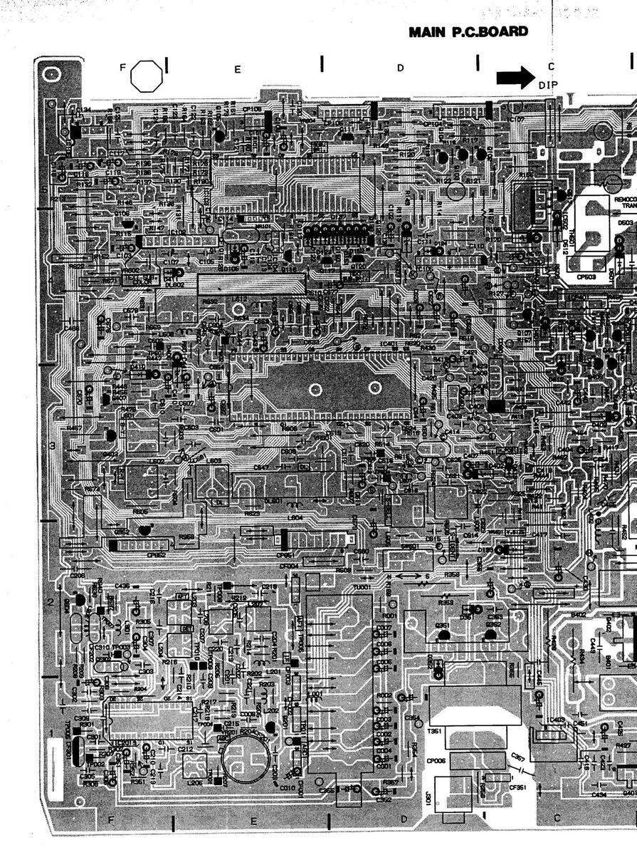
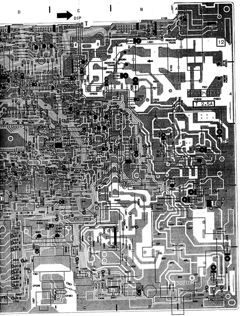
MAIN P.C.BOARD
MAIN P.C.BOARD
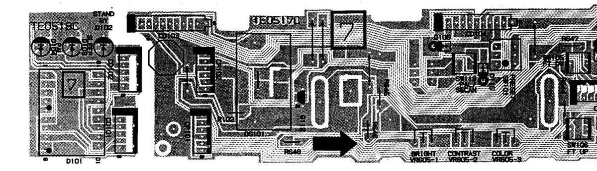
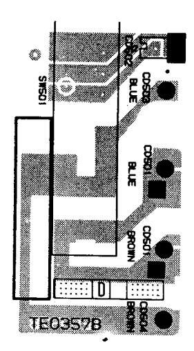
CONTROL/LED P.C.BOARD
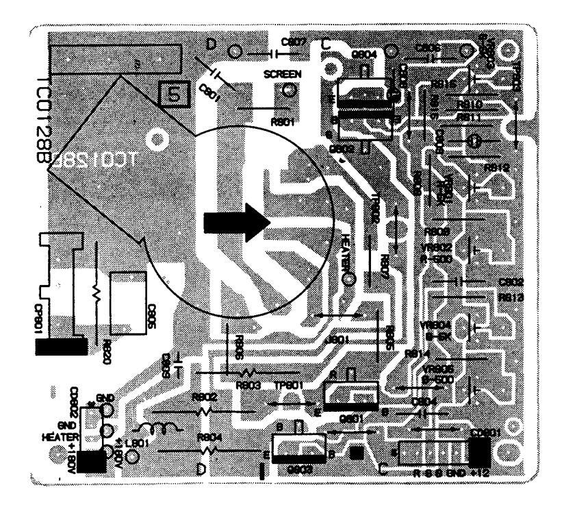
CRT P.C.BOARD
T'TEXT P.C.

/LED P.C.BOARD
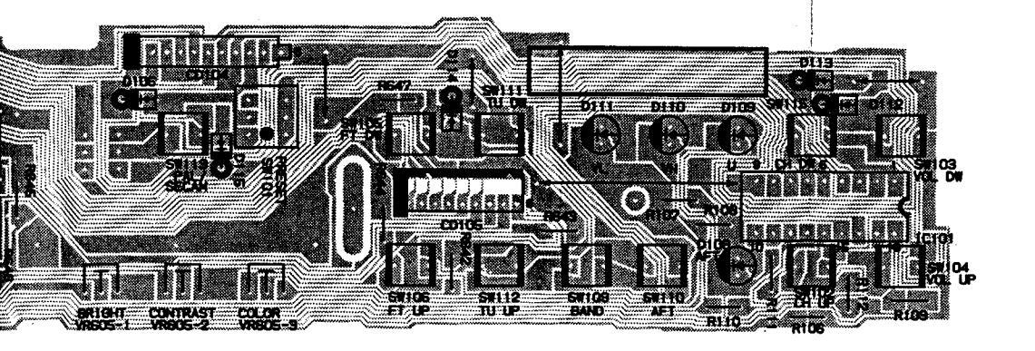
T'TEXT P.C.BOARD

POWER SWITCH P.C.BOAR
RTV servis Horvat
Kešinci, 31402 Semeljci 031-856-139 031-856-637 098-788-319
rtv-servis-horvat@os.tel.hr
Croatia
HEMATIC DIAGRAM
IRGRAM IS THE LATEST AT THE TIME SUBJECT TO CHANGE WITHOUT NOTICE.
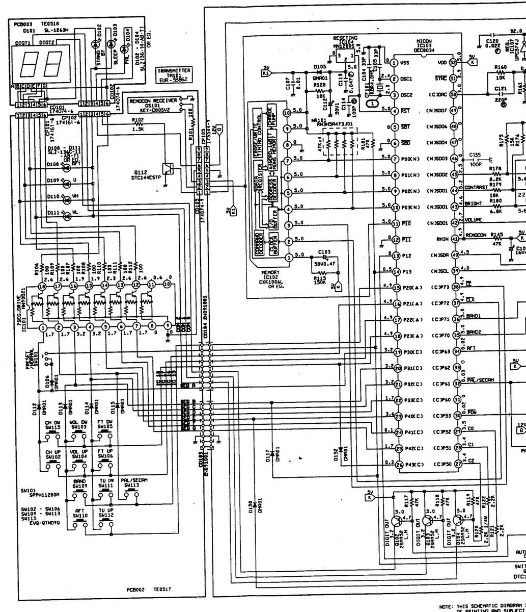
MAIN/CONTROL SCHEMATIC DIAGRAM
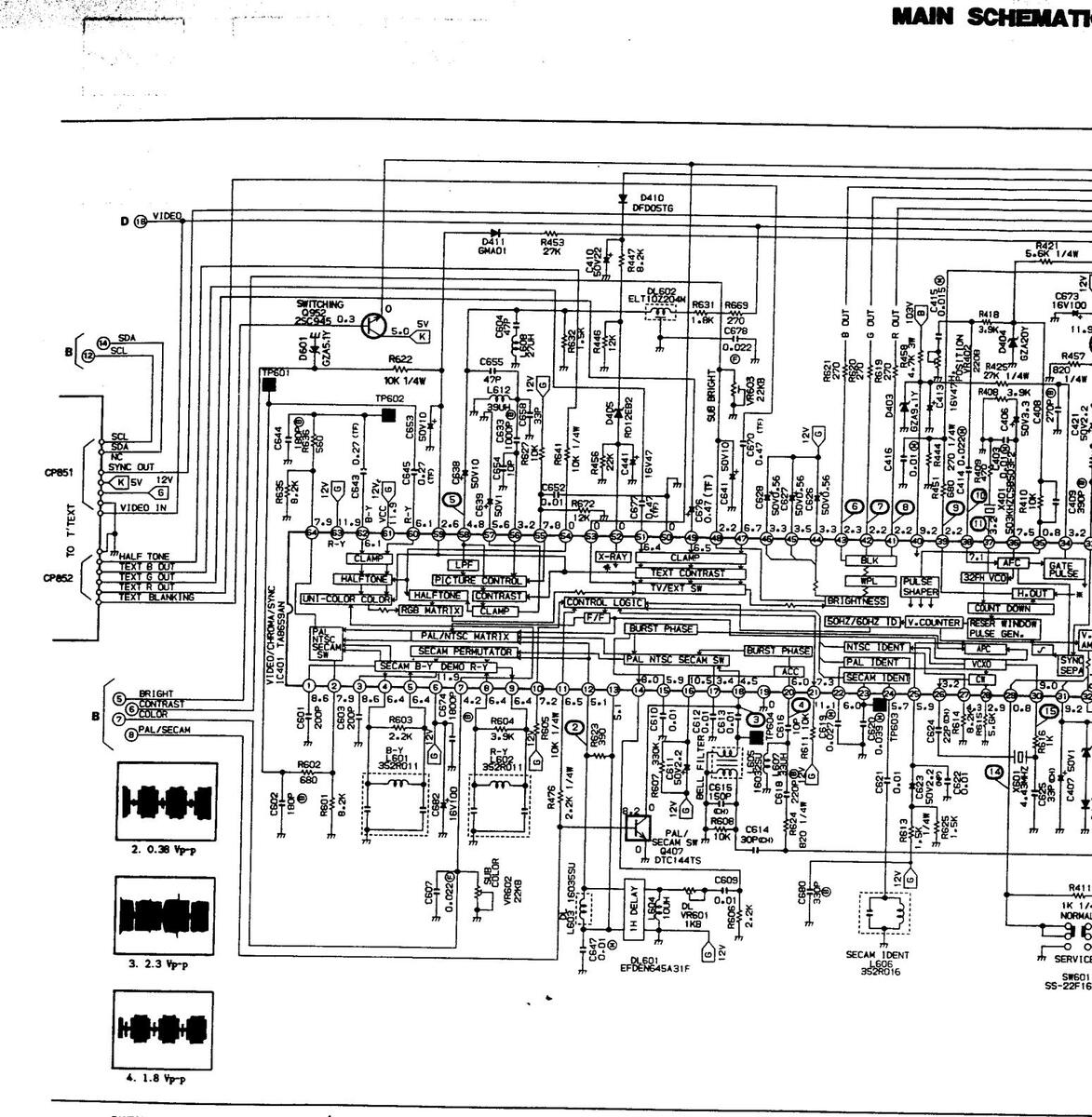
CAUTION: SINCE THESE PARTS MARKED B CRITICAL FOR SAFETY, USE DESCRIBED ON PARTS LIST ON ON
LES PIELES REPAREES PAR UN AL DANGEREUSES AN POINT DE VUE S N'UTILISER QUE CELLES DECRITE DANS LA NOMENCLATURE DES PIEC
THIS SCHEMATIC DIAGRAM IS THE LATEST AT THE TIME OF PRINTING AND SUBJECT TO CHANGE WITHOUT NOTICE
SCHEMATIC DIAGRAM

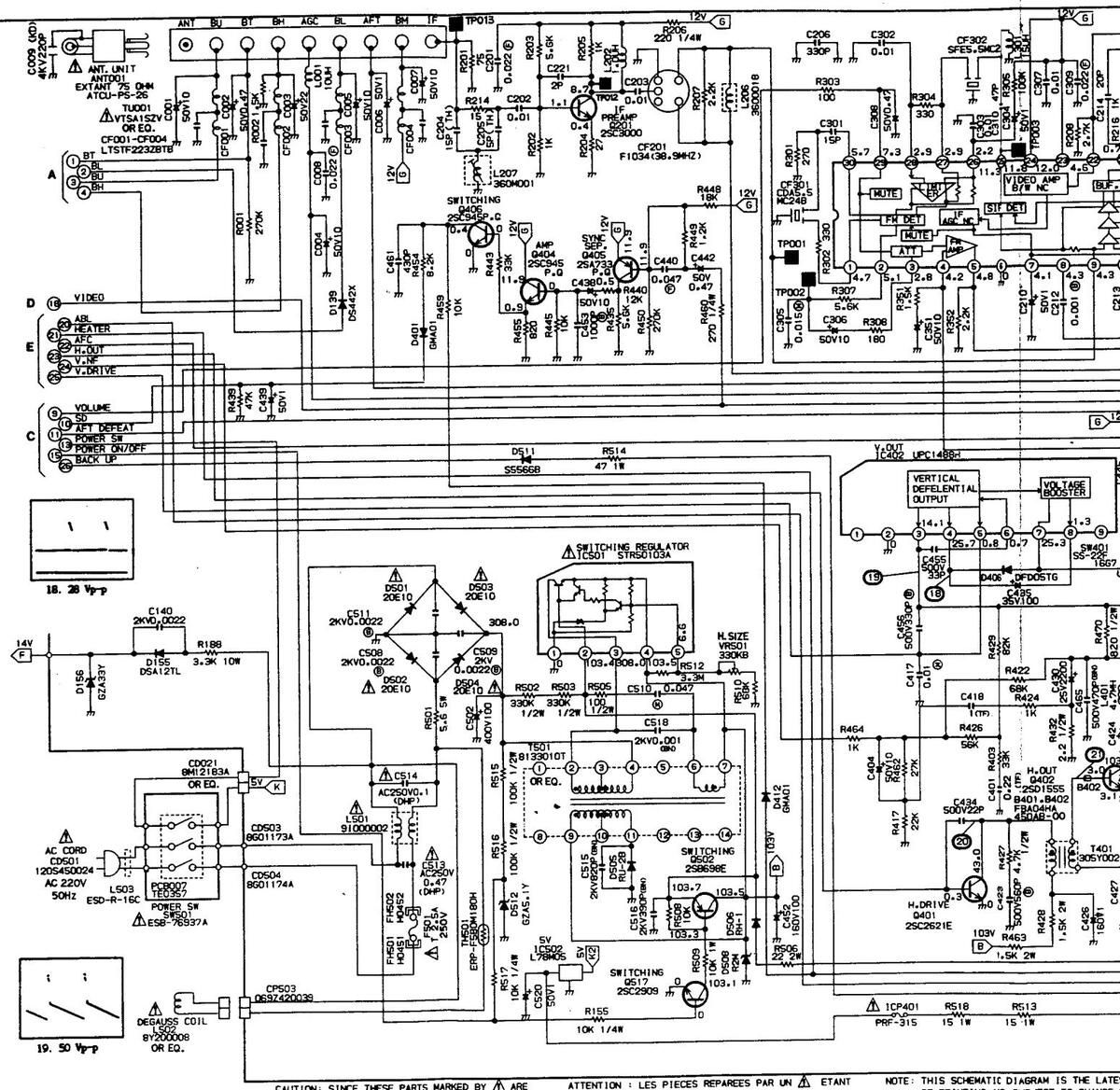
MAIN SCHEMATIC DIAGRAM
1-8630
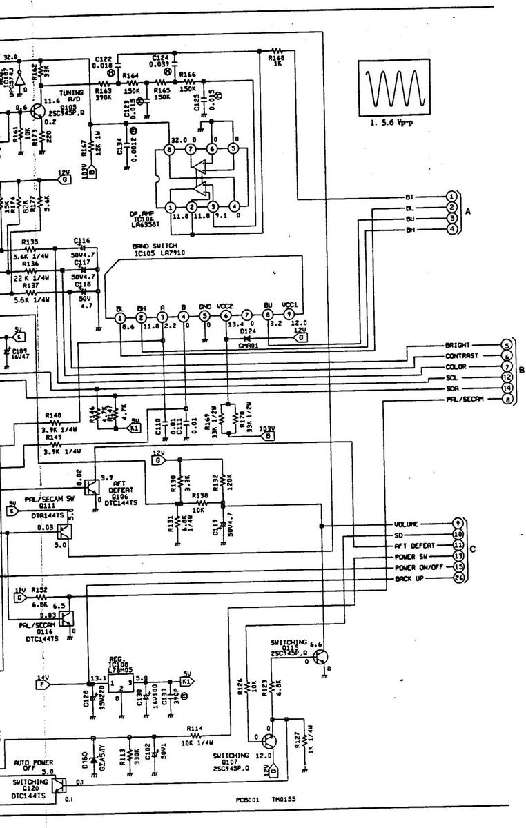
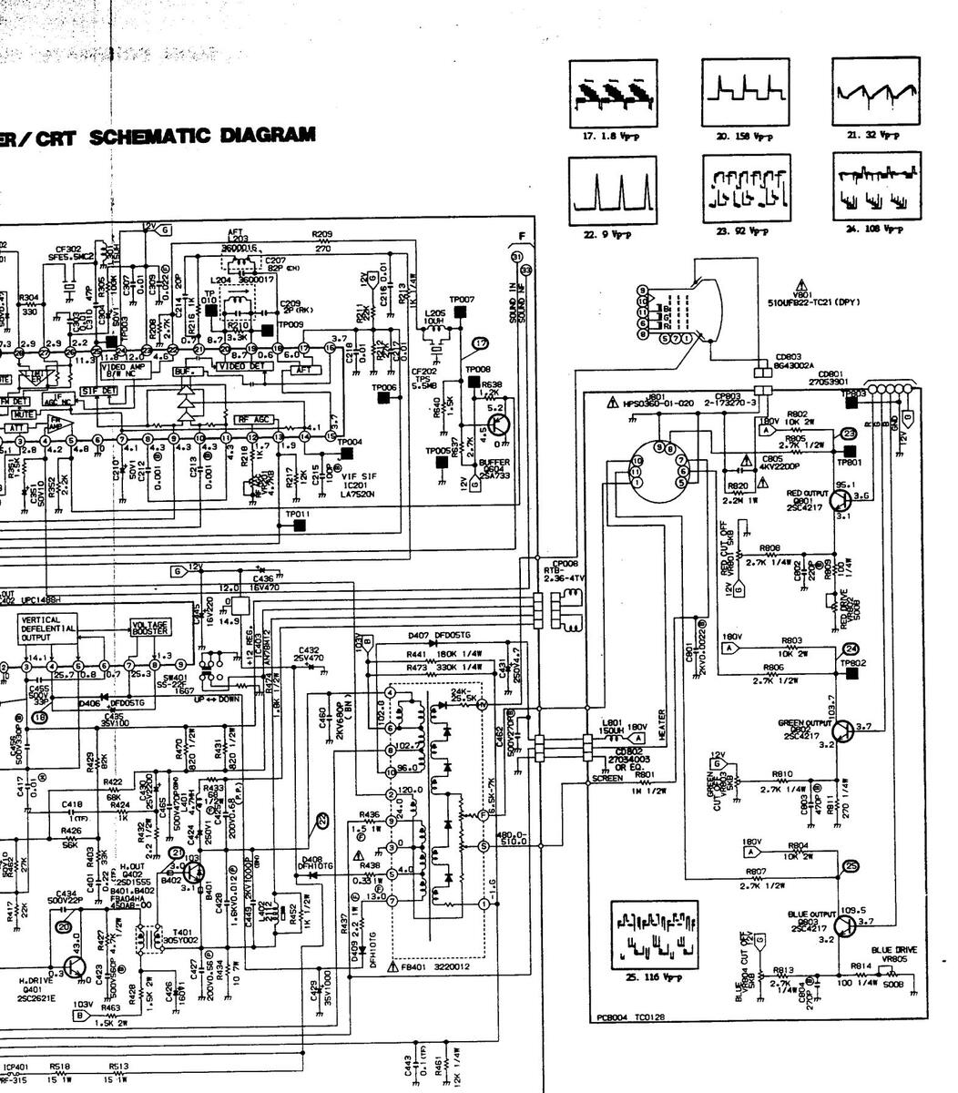
AIN/POWER/CRT SCHEMAT
PIECES REPAREES PAR UN REUSES AN POINT DE VUE
PCB TM0
MAIN/POWER/CRT SCHEMATIC DIAGRAI
TE: THIS SCHEMATIC DIAGRAM IS THE LATEST AT THE TIME OF PRINTING AND SUBJECT TO CHANGE WITHOUT NOTICE.
1-8631
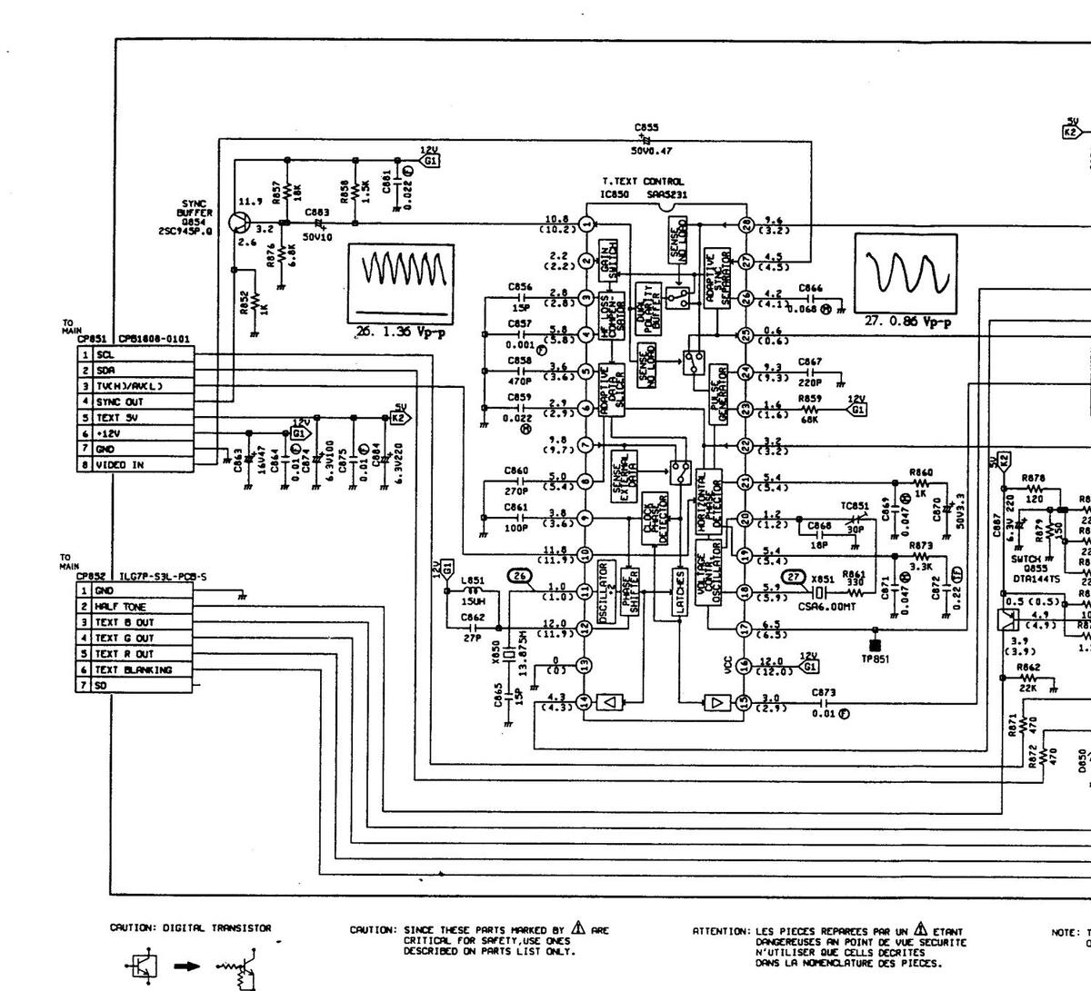
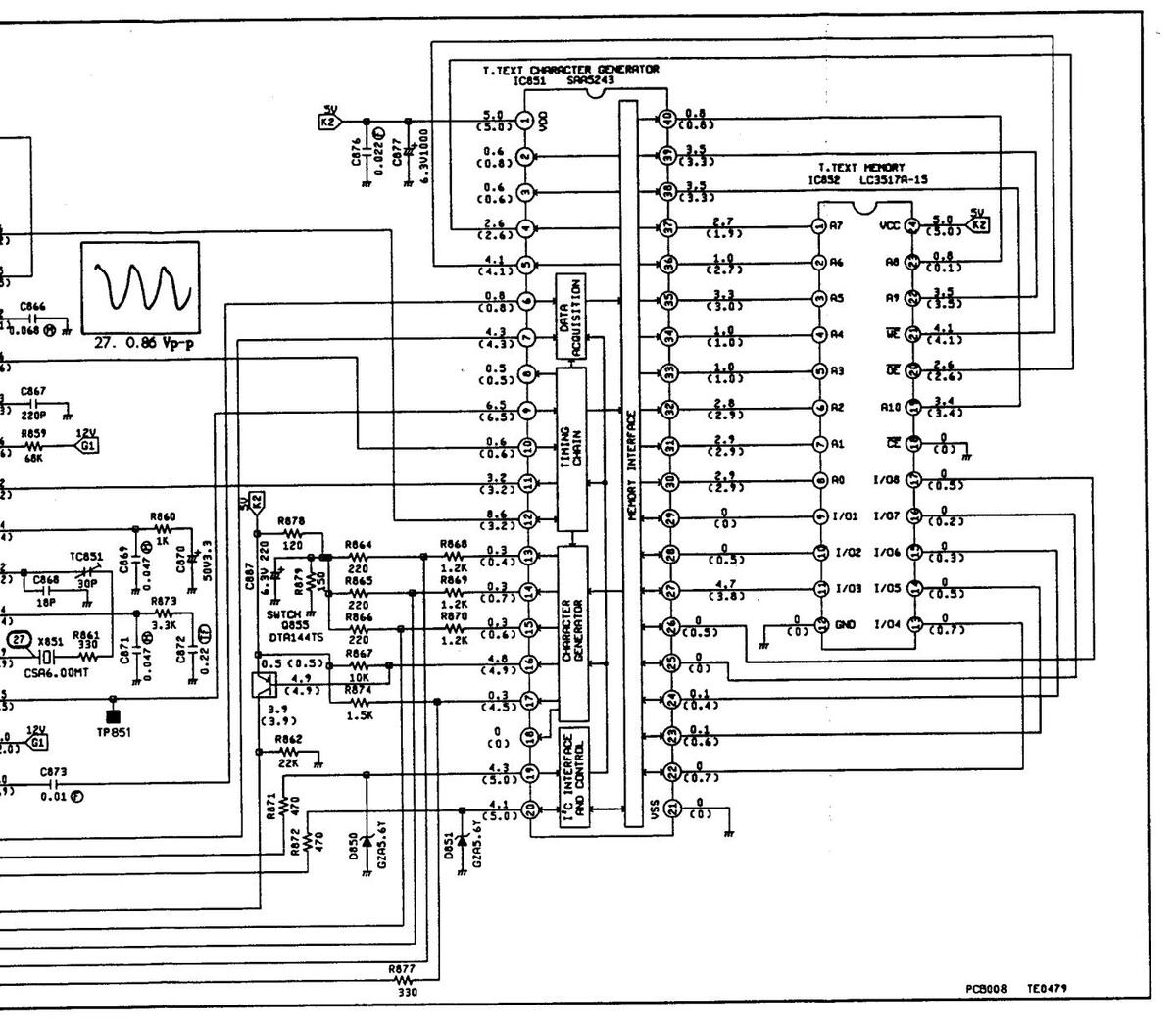
TTEXT SCHEMATIC DIAG
к.,...................................
TEXT SCHEMATIC DIAGRAM
SPIECES REPARCES PAR UN AL ETANT NOEREUSES AN POINT DE VUE SECURITE UTILISER QUE CELLS DECRITES NS LA NOMENCLATURE DES PIECES.
NOTE: THIS SCHEMATIC DIAGRAM IS THE LATEST AT THE TIME OF PRINTING AND SUBJECT TO CHANGE WITHOUT NOTICE.
NOTE: THE FIGURE WITH ( ) IS THE VOLTAGE IN NORMAL TV OPERATION. THE FIGURE WITHOUT ( ) IS THE VOLTAGE IN TELETEXT OPERETION.
T'TEXT SCHEMATIC DIA
MECHANICAL REPLACEMENT PARTS LIST
ากการการการการการการการการการการการการกา
| REF.NO | PART NO | DESCRIPTION | |
|---|---|---|---|
|
101
102 103 104 105 106 107 108 107 108 109 110 |
A35490A720
713SPD007 737SPA0002 736SPA0002 736SPA0003 A35490A740 761KSA0062 751SNA0002 751SNA0002 751SNA0001 800SR00002 |
CABINET, FRONT ASS'Y
DOOR BUTTON, CAP BUTTON, CHANNEL BUTTON, POWER CABINET, BACK ASS'Y SHEET, RATING FRAME, CRT PLATE, EARTH WIRE(3) PLATE, EARTH WIRE(2) SPRING, EARTH SHEET, CRT SUPPORT |
|
|
112
113 201 202 203 204 |
753KSA0018
749SUA0001 8117540A62 8110540B04 82A60B2161 8300560004 |
TAPPING(BO) TRUSS 4*16 BK
TAPTITE(P) TRUSS 4*20 CH WASHER 6.3*22*T1.6 SL NUT M6 |
|
|
JIAITGA02A
J3530128A J3549001A J3549003A 792SHA0009 792SHA0010 793SCD0366 |
GUARANTEE CARD
WARNING SHEET INSTRUCTION BOOK SCHEMATIC DIAGRAM PACKAGE.TOP PACKAGE.BOTTOM GIFT BOX |
||
THIS ELECTRICAL PARTS LIST IS STANDARD PART LIST, BUT INTERCHANGEABLE PARTS MAY BE USED IN THE UNIT. SEE THE INTERCHANGEABLE PARTS LIST AFTER THE STANDARD PARTS LIST. ELECTRICAL REPLACEMENT PARTS LIST
| REF.NO | PART NO DESCRIPTION | REF.NO PART NO DESCRIPTION | ||||||
|---|---|---|---|---|---|---|---|---|
| RE | SISTORS | SEMIC | ONDUCTORS (CONT) | ` | ||||
|
R167
R188 R353 R428 R428 R433 R434 R436 |
R31181123J
R5M2CF332J R31181103J R61562101J R3118A152J R61582680J R5M2CE100J R614811R5J |
R, METAL OXIDE
R.CEMENT R, METAL OXIDE R, FUSE R, METAL OXIDE R, FUSE R, CEMENT R, FUSE |
12K OHM 1W
3.3K OHM 1W 10K OHM 1W 100 OHM 1/2W 1.5K OHM 2W 68 OHM 1/2W 10 OHM 7W 1.5 OHM 1W |
D408
D409 D410 D411 D412 D413 A D501 A D502 |
D23FFH10TG
D23FFH10TG D23TFD05TG D13TGMA010 D13TGMA010 D13TGMA010 D28020E100 D28020E100 |
DIODE, RECTIFIER
DIODE, RECTIFIER DIODE, RECTIFIER DIODE, SILICON DIODE, SILICON DIODE, SILICON DIODE, SILICON DIODE, SILICON |
DFH10TG-KB4
DFH10TG-KB4 DFD05TG-BT GMA-01-BT GMA-01-BT GMA-01-BT 20E10 20E10 |
|
|
R437
R438 R458 R463 R501 R506 R509 R513 R518 R518 R802 R803 |
R615812R2J
R61481R33K R3128B472J R3118A152J R5M2CD5R6K R3118A220J R31181103J R3K181150J R3K181150J R3K181150J R3118A103J R3118A103J |
R,FUSE
R,FUSE R,METAL OXIDE R,METAL OXIDE R,METAL OXIDE R,METAL OXIDE R,METAL R,METAL R,METAL R,METAL OXIDE R,METAL OXIDE |
2.2 OHM IW
0.33 OHM IW 4.7K OHM 3W 1.5K OHM 2W 5.6 OHM 2W 22 OHM 2W 10K OHM 1W 15 OHM 1W 15 OHM 1W 10K OHM 2W |
▲ D503
▲ D504 D505 D506 D508 D511 D512 D601 D850 D851 |
D28020E100
D28020E100 D2B00RU280 D2BF00RH10 D2B000R2M0 D25T556680 D93T05R10Y D93T05R10Y D93005R60Y D93005R60Y |
DIODE, SILICON
DIODE, SILICON DIODE, SILICON DIODE, RECTIFIER DIODE, AVALANCE DIODE, RECTIFIER DIODE, ZENER DIODE, ZENER DIODE, ZENER DIODE, ZENER |
20E10
20E10 RU-2B RH-1 R2M S55668(TPE3) GZA5.1 Y BT- GZA5.6 Y GZA5.6 Y |
|
|
R804
A R820 |
R3118A103J
R03101225J C |
R, METAL OXIDE
RC APACITORS |
10K OHM 2W
2.2M OHM 1W |
1C101
1C102 1C103 1C104 |
101D10B210
130$1006L0 151D080340 1019012805 |
AN90B21
CXK1006L OEC8034 MN1280S |
||
|
C009
C134 C140 C356 C425 C427 |
C030309H2K
C0F0B04B3K C02FB07H3K E025FB07H3K P441F2684J P441F2564J |
CC
CC CC CC CE CMPP CMPP |
220 PF 4KV B
1200 PF 8 0.0022UF 2KV B 22 UF 160V 0.68 UF 200V 0.56 UF 200V |
1 C105
1 C106 1 C107 1 C108 1 C201 1 C401 |
1035079100
103D06358T 102190574J 103B98M050 103DE7520N 105DE86590 |
LA7910
LA6358T UPC574J-T Ł78M05-SA LA7520N TA8659AN |
||
|
C428
C429 C430 C431 C449 C452 |
P442F9123J
E0E7F4102M E0E7F3222M E025FD4R7M C018BN713K |
CMPP
CE CE CE CE CC |
0.012 UF 1600V
1000 UF 35V 2200 UF 25V 4.7 UF 250V 1000 PF 2KV B |
1 C402
1 C403 ▲ 1 C501 1 C502 1 C850 1 C851 1 C852 |
102SD14880
101A98M120 128490103A 103898M050 19KDF52310 14KDF52430 153D03517C |
UPC1488H
AN78M12 STR50103A L78M05-SA SAA5231 SAA5243 LC3517A-15 |
||
|
C502
C508 C509 C511 C513 C514 C515 C516 |
E0260H101T
C02FB07H3K C02FB07H3K C02FB07H3K P4440B104M P4440B104M C03BBN7W2K C01BB07N2K |
CE
CC CC CC CC CMPP CMPP CC CC CC |
100 UF 400V
0.0022UF 2KV 8 0.0022UF 2KV 8 0.0022UF 2KV 8 0.47 UF 250V 0.1 UF 250V 820 PF 2KV 390 PF 2KV 8 |
G102
Q103 Q104 Q105 Q106 Q107 Q111 Q112 |
TAST009520
TAST009520 TAST009520 TCST009450 TN7TD03002 TCST009450 TP7TD03002 TN7TD03001 |
TRANSISTOR, SILICON
TRANSISTOR, SILICON TRANSISTOR, SILICON TRANSISTOR, SILICON COMPOUND, TRANSISTOR TRANSISTOR, SILICON COMPOUND, TRANSISTOR COMPOUND, TRANSISTOR |
2SA952(C) -T
2SA952(C) -T 2SA952(C) -T 2SC945(C) -T DTC144T S 2SC945(C) -T DTA144T S DTC144ESTP |
|
|
C518
C674 C801 ▲ C805 C869 C877 C887 |
C018BN713K
C0F0804G3K C02F807H3K C03FE09H3M P1E4F0473K E0A1F0102M E08700221M |
CC
CC CC CC CP CE CE |
0.001 UF 2KV 8
1800 PF 8 0.0022UF 2KV 8 2200 PF 4KV E 0.047 UF 50V 1000 UF 6.3V 220 UF 6.3V |
Q115
Q116 Q120 Q201 Q351 Q352 Q401 |
TCST00945Q
TN7TD03002 TN7TD03002 TC3T030000 TC30041590 TC30041590 TC30026215 |
TRANSISTOR.SILICON
COMPOUND.TRANSISTOR COMPOUND.TRANSISTOR TRANSISTOR.SILICON TRANSISTOR.SILICON TRANSISTOR.SILICON TRANSISTOR.SILICON |
2SC945(C) - T
DTC144T S DTC144T S 2SC3000-AA 2SC4159 2SC2621E-PAC |
|
| SE | MICONDUCTORS | - · |
Q402
Q403 |
TD5F015550
TCST009450 |
TRANSISTOR, SILICON
TRANSISTOR, SILICON |
2SD1555
2SC945(C) - T |
||
|
D101
D102 D103 D104 D105 D106 D108 D108 |
0040322001
0021320030 0021320030 0021320030 D13TGMA010 D13TGMA010 0021320020 0021320020 |
LED DISPLAY IC
LED LED DIODE.SILICON DIODE.SILICON LED LED |
SL-1263H
SLZ136-14-AB-T1 SLZ136-14-AB-T1 SLZ136-14-AB-T1 GMA-01-BT GMA-01-BT SLZ-136C-11-AB-T1 SLZ-136C-11-AB-T1 |
Q404
Q405 Q406 Q407 Q502 Q517 Q604 |
TCST009450
TAST007330 TCST009450 TN7TD03002 TB3T00698E TC3T029090 TAST007330 |
TRANSISTOR, SILICON
TRANSISTOR, SILICON TRANSISTOR, SILICON COMPOUND, TRANSISTOR TRANSISTOR, SILICON TRANSISTOR, SILICON TRANSISTOR, SILICON |
2SC945(C)-T
2SA733(C)-T 2SC945(C)-T DTC144T S 2SB698E-AA 2SC2909 2SA733(C) |
|
|
D110
D111 D112 D113 D114 D115 |
0021320020
0021320020 D13TGMA010 D13TGMA010 D13TGMA010 D13TGMA010 |
LED
LED DIODE,SILICON DIODE,SILICON DIODE,SILICON DIODE,SILICON |
SL Z-136C-11-AB-T1
SL Z-136C-11-AB-T1 GMA-01-BT GMA-01-BT GMA-01-BT GMA-01-BT |
Q802
Q803 Q854 Q855 Q952 |
TC3F042170
TC3F042170 TC3F042170 TC5T009450 TP7TD03002 TCST009450 |
TRANSISTOR, SILICON
TRANSISTOR, SILICON TRANSISTOR, SILICON TRANSISTOR, SILICON COMPOUND, TRANSISTOR TRANSISTOR, SILICON |
2504217-HAC
2504217-RAC 2504217-RAC 25045(0)-T DTA144T 250945(0)-T |
|
|
D117
D124 D139 D150 D152 D155 |
D131GMA010
D13TGMA010 D13TGMA010 D13TGMA010 D13TGMA010 D23HDSA12T |
DIODE, SILICON
DIODE, SILICON DIODE, SILICON DIODE, SILICON DIODE, RECTFIER |
GMA-01-B1
GMA-01-BT DS442X-BT GMA-01-BT GMA-01-BT DSA12TL-FB2 |
L001
L202 L203 L204 L205 |
021JA6100K
0216731R0M 033600016N 033600017N 021JA6100K |
COIL
COIL, VIDEO IFT COIL, VIDEO IFT COIL, VIDEO IFT |
10 UH
1.0 UH 3600016 3600017 10 UH |
|
|
D156
D160 D351 D352 D401 D402 D403 D403 |
D93003300Y
D93T05R10Y D13TGMA010 D13TGMA010 D13TGMA010 D93T07R50Y D93T09R10Y |
DIODE.ZENER
DIODE.SILICON DIODE.SILICON DIODE.SILICON DIODE.SILICON DIODE.ZENER DIODE.ZENER DIODE.ZENER |
GZA33 Y
GZA5.1 Y GMA-01-BT GMA-01-BT GZA7.5 Y BT GZA9.1 Y BT GZA9.1 Y BT |
L206
L207 L301 L401 L402 A L501 A L502 |
033600018C
03360M001N 021JA6150K 021679472K 0221000012 0291000002 028Y200008 |
COIL, VIDEO IFT
COIL, TRAP COIL COIL COIL, LINEARITY COIL, LINE FILTER COIL, DEGAUSS |
3600018
360M001 15 UH 4.7 MH 2112 91000002 8Y200008 |
|
|
D405
D406 D407 |
D92T012082
D23TFD05TG D23TFD05TG |
DIODE, ZENER
DIODE, RECTIFIER DIODE, RECTIFIER |
RD12EB 2 TA11R
DFD05TG-BT DFD05TG-BT |
L 503
L 601 L 602 |
02AXA509C1
03352R011S 03352R011S |
FILTER LINE
COIL, CHROMA COIL, CHROMA |
ESD-A-16C
352R011 352R011 |
|
16
ALC: NEW AVE

| NIS LISI | ||||||||||
|---|---|---|---|---|---|---|---|---|---|---|
| 1 | REF.NO | PART NO | DESCRIPTION | REF.NO | EF.NO PART NO DESCRIPTION | |||||
| COILS & | TRANSFORMER | S (CONT) | MISC | ELLANEOUS (CONT) | ||||||
|
ON
>FH10T0-KB4 >FH10TG-KB4 FD05TG-BT MA-01-BT MA-01-BT 0E10 0E10 0E10 0E10 0E10 |
L603
L604 L605 L606 L607 L608 L612 L801 L851 L851 T351 T351 T501 |
03352R007S
021JA6100K 03302R001S 03352R016S 021JA6330K 021JA6370K 021JA6370K 021JA6270K 021JA6390K 021JA2151K 021Z73150K 045128007U 03305Y002S 048133010T |
COIL. CHROMA
COIL COIL. CHROMA COIL. CHROMA COIL COIL COIL COIL COIL TR. SOUND OUTI TRANS. HORIZOI TRANSFORMER. SU |
160355U
10 UH 160325U 352R016 33 UH 27 UH 39 UH 150 UH 15 UH G PUT 5128007 NTAL DRIVE 3057002 WITCHING $133010 |
50
r |
CF202
CF301 CF302 CF351 CP006 CP008 CP101 CP102 CP105 CP503 CP803 CP851 CP852 D1601 |
202 1012105R51 301 101225R501 302 1012005R52 351 116F3TH4Z1 006 069Z340018 101 0694260090 102 0694260090 105 0694290260 303 0694420039 303 0694430100 501 0690180179 551 0690180179 552 069H170209 |
FILTER.CERAMIC TRAP
FILTER.CERAMIC FILTER.CERAMIC FILTER.ERMI CONNECTOR PCB SIDE CONNECTOR PCB SIDE CONNECTOR PCB SIDE CONNECTOR PCB SIDE CONNECTOR PCB SIDE CONNECTOR PCB SIDE CONNECTOR PCB SIDE CONNECTOR PCB SIDE |
TPS5.5MB
CDA5.5MC24B SFE5.5MC2 LTSTF232BTB RTB-2.36-2TV RTB-2.36-4TV 174161-6 175544-9 0692420039 2-173270-3 CPB1808-0101 1LG7P-S3L-PCB-S |
|
|
U-28
H-1 |
J301 | 0602101004 | JACK. RCA 3.5 | HSJ0912-01-05 |
DL 602
EAR351 |
1035000402
074U130009 |
DELAY LINE GLASS |
EFDEN645A31F
ELT10Z204M 4U130009 |
||
|
2M
55668(TPE3) ZA5.1 Y BT- |
7 7901 | 0662130007 | SWITCHES | HPS0360-01-02 | 2 |
F501
F8401 FH501 |
0808T2R502
0432200121 067M0T0004 |
FUSE
TRANSFORMER, FLYBACK HOLDER, FUSE |
T 2.5A 250V
3220012 H0451 |
|
|
ZA5.6 Y
ZA5.6 Y V90821 412805 A7910 A6356T 26574J-T '8M05-SA (7520) 4855 |
SW101
SW102 SW103 SW104 SW105 SW105 SW105 SW106 SW109 SW110 SW111 SW112 SW113 SW115 |
0501201007
0504101T13 0504101T13 0504101T13 0504101T13 0504101T13 0504101T13 0504101T13 0504101T13 0504101T13 0504101T13 0504101T13 |
SWITCH, PUSH
SWITCH, TACT SWITCH, TACT SWITCH, TACT SWITCH, TACT SWITCH, TACT SWITCH, TACT SWITCH, TACT SWITCH, TACT SWITCH, TACT SWITCH, TACT |
SPPH11280A
EVG-GTNO9G EVG-GTNO9G EVG-GTNO9G EVG-GTNO9G EVG-GTNO9G EVG-GTNO9G EVG-GTNO9G EVG-GTNO9G EVG-GTNO9G EVG-GTNO9G EVG-GTNO9G |
4 |
FH502
A 1CP401 MS002 NR101 OS101 S001 SP351 TC851 TH501 TH501 TH101 A 1U001 V801 |
067M0T0005
084E00R301 128B000017 110E447301 077M006004 128F100003 070B043001 0100514001 0810M180H0 076100Q006 0145P11004 |
HOLDER, FUSE
IC PROTECTOR MICA, SHEET R, NETWORK REMOTE RECEIVER SPACER SPEAKER C, CERAMIC TRIMMER DEGAUSS ELEMENT TRANSMITTER TUNER, UHF-VHF |
H0452
PRF-315 STR-50103M1CA RN3H5A473J01 KEY-C00SV2 BUSH-M C100A21K2453 TZ03R300E ERP-F580M180H EUR-53862 VTSA1SZV |
|
| C1488H | 4 |
SW401
SW501 SW601 |
0510B22001
0530102008 0510B22001 |
SWITCH.SLIDE
SWITCH.PUSH SWITCH.SLIDE |
SS-22F16G7
ESB-76937A SS-22F16G7 |
X401
X601 X850 |
1002R50301
10064R4382 100613R801 |
CERAMIC.OSCILLATOR
CRYSTAL HC-49/U CRYSTAL HC-49/U |
5100F822-TC21
CS8503F2 4.43361875MHZ |
|
|
850103A
8005-5A 45231 |
VARIA | BLE RESISTOR | IS | X851 | 10026R0004 | SERALOCK | CSAS. COMT | |||
|
A5243
3517A-15 A952(C)-T A952(C)-T C945(C)-T C144T S C945(C)-T C944T S A144T S |
VR201
VR401 VR402 VR501 VR602 VR603 VR603 VR801 VR802 |
V1163Q3B02
V1163Q4B03 V1163H2B02 V1263L5B01 V116313B02 V1163H4B02 V1163H4B02 V1163H4B02 V1163H4B02 V175C53B01 V175C53B03 |
VR, SEMIFIXED
VR, SEMIFIXED VR, SEMIFIXED VR, SEMIFIXED VR, SEMIFIXED VR, SEMIFIXED VR, SEMIFIXED VR, SEMIFIXED VR, SEMIFIXED |
EVN-D4AA00BQ3
EVM4LGA00BQ4 EVN-D4AA00BE2 RH0615CN5J0F EVN-D4AA00B13 EVN-D4AA00BE4 EVN-D4AA00BE4 RVA0911H304-1-50 RVA0911H304-1-50 |
M | |||||
|
C144ESTP
C945(C)-T Q C144T S |
VR804
VR805 |
V175C53803
V175C52803 |
VR. SEMIFIXED |
RVA0911H304-2-50
RVA0911H304-3-50 RVA0911H304-3-50 |
M
M M |
|||||
| C144T S | • P.C. | BOARDS ASS'Y | ||||||||
|
C3000-AA
C4159 C4159 2621E-RAC D1555 C945(C)-T C945(C)-T Q45(C)-T Q33(C)-T Q |
PCB001
PCB002 PCB003 PCB004 PCB007 PCB008 |
A35490A01AC
A35490A03A A35490A20A A35490A11A A35490A15A A35490A15A MI |
PCB ASS'Y
PCB ASS'Y PCB ASS'Y PCB ASS'Y PCB ASS'Y PCB ASS'Y SCELL ANFOLIS |
TM0155-C
TE0517 TE0518 TC0128 TE0357 TE0479 |
||||||
|
2144T S
1698E-4A 12909 733 4217-RAC 4217-RAC 4217-RAC 4217-RAC 945(C)-T 144T S 945(C)-T UH UH 2016 |
ANT001
8401 8402 8T101 8T102 CD006 CD021 CD102 CD102 CD103 CD104 CD105 CD501 CD503 CD504 CD504 |
0637300013
024JT03551 024JT03551 141T003004 141T003004 068G32001A 068M12183A 0694260080 0694260080 122N091001 122N091001 122N091001 0694290080 1205450024 068G01173A 068G01173A |
ANT. UNIT
CORE, BEADS CORE, BEADS CORE, BEADS BATTERY, MANGAN BATTERY, MANGAN CORD LIS CONNECTOR CONNECTOR PCB CONNECTOR PCB CONNECTOR PCB CONNECTOR PCB CONNECTOR PCB CORD, JUMPER CONNECTOR PCB CORD, AC CORD CONNECTOR |
ATCU-PS-26
FBA04HA450AB-( UM-3 1.5V UM-3 1.5V UM-3 1.5V CTOR 8032001A 8M12183A SIDE 174074-6 2N091001 SIDE 174074-6 2N091001 SIDE 174074-9 1205450024 8G01173A |
00 |
RI
F |
ESISTOR
RCCA APACITORS CCCE |
RBON RESISTOR | ||
|
2017
UH 2018 WH001 UH MH 2 20002 20008 -R-16C R011 1011 |
CD801
CD802 CD803 CF001 CF002 CF003 CF004 CF101 CF201 |
1227053901
1227034003 068043002A 116F3TH4Z1 116F3TH4Z1 116F3TH4Z1 116F3TH4Z1 116F3TH4Z1 1003T4R001 1027038R91 |
CORD, JUMPER
CORD, JUMPER CORD UX CONNECT FILTER, EMI FILTER, EMI FILTER, EMI CERAMIC OSCILLA FILTER, SAW |
27053901
27034003 TOR 8G43002A LTSTF223ZBTB LTSTF223ZBTB LTSTF223ZBTB LTSTF223ZBTB LTSTF223ZBTB LTSTF223ZBTB STOR KBR-4.0MSTF F1034 |
CEAL
CPPO CPPPO CPLPL CMPME CMPLME CMPPME STST |
UMI ELECTROLYTIC CAP
LYESTER CAPACITOR LYPROPYLENE CAPACITOR ASTIC CAPACITOR TAL POLYESTER CAPACI TAL PLASTIC CAPACITO TAL POLYPROPYLENE CA YROL CAPACITOR |
ACITOR
R TOR R PACITOR |
|||
INTERCHANGEABLE PARTS LIST
NOTE: THE FOLLOWING PART(S) MAY BE SUBSTITUTED FOR PARTS INDICATED IN THE BASIC PART(S) LIST (WITH THE SAME REF.NO.). THESE PARTS SHARE THE SAME ELECTRICAL CHARACTERISTICS AND OTHER ELEMENTS FOR COMMON USAGE. EITHER PART NUMBER MAY BE USED IN THIS UNIT.
| REF.NO |
DESCRIPTION
(PART NO) |
DESCRIPTION
(PART NO) |
|
CD021
CD802 |
8M12183A
(068M12183A) 27034003 (1027034002) |
8G12183A
(068G12183A) 2Q034002 (122Q034002) |
| EAR351 |
(1227034003)
4U130009 (074U130009) |
SE100-335
(074N130007) CXK1008L |
| ▲ L502 |
(13051006L0)
8Y200008 (028Y200008) |
(13051008L0)
8J200008 (028J200008) 028J200008) |
|
5P351
T501 |
C100A21K2453
(070B043001) 8133010T (04133010T) |
(070R143004)
8133010 (0481330105) |
| ₫ тиоо1 |
VTSA1SZV
(0145P11004) |
VTSA1SZV
(0145J11004) |
THE LISTED PARTS ARE INTERCHANGEABLE WITH ONE COMPLETE BLOCK AS FOLLOWS.
| ONE COM | |||
|---|---|---|---|
| ſ | REF.NO |
DESCRIPTION
(PART NO) |
DESCRIPTION
(PART NO) |
|
D102
D103 D104 D108 D109 D110 D111 |
SLZ136-14-AB-T1
(002132Q030) SLZ136-14-AB-T1 (002132Q030) SLZ136-14-AB-T1 (002132Q030) SLZ-136C-11-AB-T1 (002132Q020) SLZ-136C-11-AB-T1 (002132Q020) SLZ-136C-11-AB-T1 (002132Q020) SLZ-136C-11-AB-T1 (002132Q020) |
LN&1RCPH-(C)
(0021121050) LN&1RCPH-(C) (0021121050) LN&1RCPH-(C) (0021121050) LN&1RCPH-(C) (0021121050) LN&1RCPH-(C) (0021121050) LN&1RCPH-(C) (0021121050) LN&1RCPH-(C) (0021121050) |
|


 Loading...