

COLOR TELEVISION RECEIVER

ORION Color 5188-2 RC Color 1550-2 RC
KENDO CTV 90-20
MFR'S Version: G

CONTENTS
| PAGE | |
|---|---|
| SPECIFICATIONS | 1 |
| MAJOR COMPONENTS LOCATION GUIDE | 2 |
| ALIGNMENT INSTRUCTIONS | 3~5 |
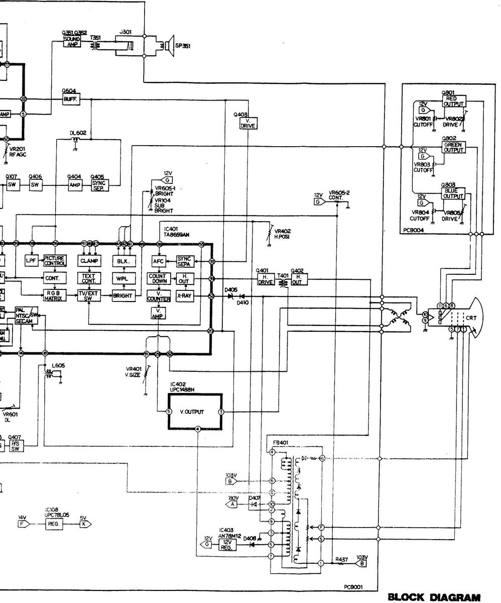
| BLOCK DIAGRAM | 6 |
| MAIN P.C.BOARD | 7 |
| CONTROL / LED / POWER SWITCH / CRT P.C. BOARDS | 8 |
| CHASSIS SCHEMATIC DIAGRAMS | 9~11 |
| MECHANICAL EXPLODED VIEW | 12 |
| MECHANICAL REPLACEMENT PARTS LIST | 13 |
| ELECTRICAL REPLACEMENT PARTS LIST | 14,15 |
| INTERCHANGEABLE PARTS LIST | 16 |
SPECIFICATIONS
| PICTURE SIZE | 20 inch |
|---|---|
| SYSTEM | PAL/SECAM |
| FREQUENCY RANGE VHF(L) | 2 - 4 X - 52 ch 47 - 118 MHz |
| VHF(H) | C2 C10 E 10 C11 - C20 ch |
| 53 - 510, 5 - 12, 511 - 520 cm | |
| 118 - 300 MHz | |
| UHF | 21 - 69 ch, 470 - 862 MHz |
| MAXIMUM SENSITIVITY VHF | 20 dB |
| UHF | 25 dB |
| INTERMEDIATE FREQUENCY: | |
| Picture IF Carrier Frequency | 38.9 MHz |
| Color Sub Carrier Frequency | 34.47 MHz |
| Sound IF Carrier Frequency | 33.4 MHz |
| SOUND INTERMEDIATE FREQUENCY | 5.5 MHz |
| MAXIMUM OUTPUT POWER | 2.0 W |
| 10% THD OUTPUT POWER | 1.8 W |
| POWER SOURCE | AC 220V |
- IMPORTANT
*FOR SERVICE WORK ALWAYS USE MAINS ISOLATING TRANSFORMER, CHASSIS IS LIVE. (IRRESPECTIVE OF POLARITY OF MAINS PLUG.)
*IN CASE OF REMOVING PCB OR SOMETHING, AFTER UNFASTENING THE WIRE OR CHANGING THE WIRE POSITION, IT IS IMPORTANT TO PUT THE FASTENING OF WIRE AND THE POSITION OF WIRE AS IT WAS. BECAUSE, PICTURE DISTORTION OR SOMETHING MAY APPEAR ON THE DISPLAY. SO, BE SURE TO CONFIRM THE FASTENING AND POSITION OF WIRE BEFOREHAND. THEN START TO THE OPERATION.
*INFERIOR SILICON GREASE CAN DAMAGE IC'S AND TRANSISTORS. WHEN REPLACING AN IC OR TRANSISTOR, USE ONLY SPECIFIED SILICON GREASE (YG6260). REMOVE ALL THE OLD SILICON BEFORE APPLYING NEW SILICON.
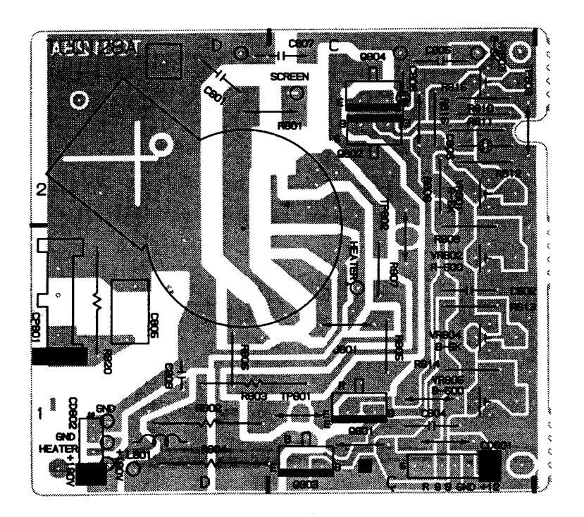
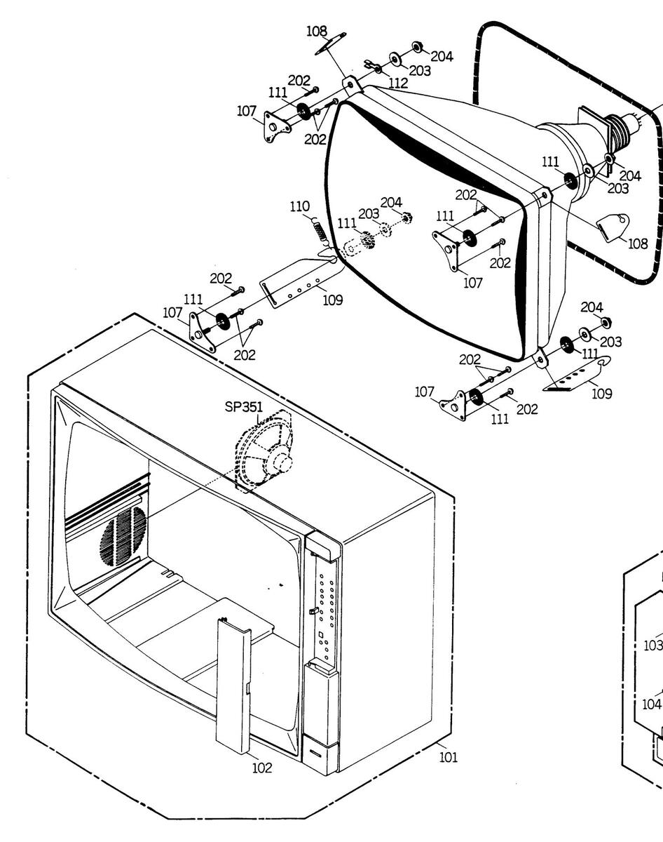
MAJOR COMPONENTS LOCATION GUIDE

2
SHUT DOWN CIRCUIT
When the high voltage rises, a simultaneous voltage increase will develop at terminal 9 of the Horizontal Output Transformer(FB401), and be applied to pin 52 of IC401. If excessive high voltage is produced, the increased voltage developed exceeds the rating of zener diode D405 causing the Horizontal Oscillator to stop functioning and the high voltage system to shut down.
HORIZONTAL AND VERTICAL SIZE ADJUSTMENT
Adjust the control (VR501) and (VR401) so that the picture fills the picture from top to bottom and is proportionate to the width.
RE AGC ADJUSTMENT
Contraction of the second
The RF AGC control is adjusted at the factory and rarely requires re-adjustment unless the received picture exhibits too much snow or the receiver lacks sensitivity. Home adjustment can be made by tuning in a weak snowy station and adjusting RF AGC for the least amount of snow. For a more accurate adjustment, use the following procedure
- Receive the test pattern signal (80dB). Adjust AGC pin of TV tuner (TPG11) to 4.75V with VR201 control.
CHR BRIGHT ADHISTMENT
- Receive the signal of Monochrome pattern. Set the Bright (VRC05-1) control to minimum position and Contrast (VRC05-2) control to maximum position. Adjust the Sub Bright (VR104) control to obtain a dim white pattern on 75% of gray scale.
FOCUS ADJUSTMENT
Adjust focus control on the flyback transformer for a defined picture.
HUE DELAY ADJUSTMENT
- Receive the signal of DEM pattern. Connect dual oscilloscope to IP601 and IP602. Adjust waveform to straight line with VR601 and L603.

AFT ADJUSTMENT
- 1. Connect the output of the oscillator to the tuner pack
- 2. Adjust L203 to keep constant DC voltage at TPCO6 with AFT ON and AFT OFF.
HORIZONTAL POSITION ADJUSTMENT
Receive the test pattern signal. (PAL Philips) Adjust horizontal picture position to center with VR402.
COLOR PURITY ADJUSTMENT
The receiver must be operated 10 minutes prior to this procedure and the face plate of the CRI must be at room temperature. The following procedure is ecommended while using a Dot/Bar Generator. Check for correct location of all neck components. (Refer to Fig. 1) Rough-in the static convergence at the center of the CRI, as explained in the static convergence.
- Rotate the contrast control to maximum CCW position and rotate brightness control as far CW as possible without causing the picture to "bloom". Rotate the Red (VR801) and Blue (VR804) Cut off controls to maximum CCW position. Rotate the Green (VR803) Cut off control sufficiently in a CW direction Loosen the deflection yoke clamp screw and pull the deflection yoke toward the rear of the CRI. Begin the following adjustment with the tabs on the round purity magnet rings set together, slowly separate the two tabs while at the same time rotating them to adjust for a uniform green stripe at the center of the CRI screen. Carefully slide the deflection yoke forward to achieve green (uniform green screen). NOTE: Center purity is obtained by adjusting the tabs on the round purity magnet rings, outer edge purity is obtained by sliding the deflection yoke forward. Check for red and blue field purity by reducing the output of the Green (VR803) Cut off control and alternately increasing output of Red (VR801) and Blue (VR804) Cut off controls and touch-up adjustments, if required.
-
- required. 9. Tighten deflection yoke clamp screw

Fig. 1 Picture Tube Neck Component Location
BLACK AND WHITE TRACKING
The purpose of this procedure is to adjust the bias applied to the picture tube to obtain good black and white picture production at all brightness levels while, at the same time achieving maximum useable brightness. Proper RF AGC control adjustment should have been verified prior to performing this procedure.
- With antenna connected to the receiver, go to a channel with strong reception. Adjust the fine tuning control so that the receiver will not produce a color picture while the following adjustment are being performed. Rotate the Red (VR802) and Blue (VR805) Drive control fulley CW and then back CCW to the center of their rotation ranges. Rotate the Green (VR803), Red (VR801) and Blue (VR804) Cut off controls to the fully CCW end of their rotation
- Gut off controls to the fully CCW end of their rotation ranges. 4. Set normal-service switch to service position. Adjust the voltage of test point (collector of green output transistor on CRI PCB) to DCI50V with brightness control. Voltage measurement should be measured with an oscilloscope. 5. Rotate the screen control to the fully CCW end of its rotation range. Then, rotate it CV until a dim line of one pronounced color (green, red or blue) is obtained.
-
6. The other two color Cut off controls must be rotated CW until a dim white line is obtained.
7. Set normal-service switch to normal position.
8. If required, perform touch-up adjustment of the Red (VR802) and Blue (VR805) Drive controls to produce a uniform monochrome picture.
9. Rotate the brightness and contrast controls fully CCW.
10. Rotate the brightness control CW until a dim raster is obtained.
11. If the second data set dimension of the rest.
- optained. 11. If the screen does not display with uniformity, steps 2 through 10 of this procedure must be repeated.
STATIC CONVERGENCE ADJUSTMENT
- 1. Switch the Receiver ON and allow it to warm up for 15
- 2.
- Switch the Receiver ON and allow it to warm up for 15 minutes. Connect the output of a Crosshatch Generator to the receiver and concentrating on the center of the CRI screen, proceed as follows: Locate a pair of 4 pole magnet rings. Rotate individual rings (change spacing between tabs) to converge the vertical red and blue lines. Rotate a pair of rings (maintaining spacing between tabs) to converge the horizontal red and blue lines. After completing red and blue center convergence, locate a pair of 6 pole magnet rings. Rotate individual rings (change spacing between tabs) to converge the vertical red and blue (magenta) and green lines. Rotate a pair of rings (maintaining spacing between tabs) to converge the horizontal red and blue (magenta) and green lines.
DYNAMIC CONVERGENCE ADJUSTMENT
Dynamic convergence (convergence of the three color fields at the edges of the CRI screen) is accomplished by proper insertion and positioning of three rubber wedges between the edge of the deflection yoke and the tunnel of the CRI. This is accomplished in the following manner.
- 1. Switch the Receiver ON and allow it to warm up for 15
-
Switch the Receiver ON and allow it to warm up for 15 minutes.
Apply crosshatch pattern from Dot/Bar Generator to receiver. Observe spacing between lines around edges of CRI screen.
Tilt the deflection yoke up or down, and insert tilt adjustment wedges (1) and (2) between the deflection yoke and the CRI until the improper convergence illustrated in Fig. 2 (A) has been corrected.
Tilt the deflection yoke right and left, and insert tilt adjustment wedge (3) between the deflection yoke and the CRI until the improper convergence illustrated in Fig. 2 (B) has been corrected.
Alternately change spacing between, and depth of insertion of the three wedges proper dynamic convergence is obtained.
Use a strong adhesive tape to firmly secure each of the three wedges to the funnel of the CRI.
Check purity and adjust, if necessary.

Fig. 2 Dynamic Convergence Adjustment
VIDEO IF AND TRAP ALIGNMENT
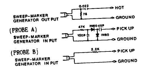
VIDEO IF AND TRAP ALIGNMENT TEST EQUIPMENT CONNECTION OSCILLOSCOPE .... Set AC-DC SWEEP-MARKER GENERATOR .... Connect H SCOPE and V SCOPE output cable from SWEEP-MARKER GENERATOR to H and V input connectors on the OSCILLOSCOPE, connect hot lead of SWEEP-MARKER OUTPUT cable to test point TPOOI on PCBOOI; connect ground lead to chassis ground. (Dromet B) between TPOO4, B+
- 1. Connect 10K ohm variable resistor between IP004. B+
-
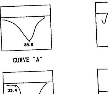
Connect 10K ohm variable resistor between TPOO4, B+ (12V) to ground. Install AGC VR to prevent saturation in waveform, then adjust AGC VR for proper size of waveform. On the other hand, in case IF AGC voltage is supplied externally, adjust for proper size of waveform on condition that IF AGC voltage is within 10V and is gradually decreased. Adjust L204 to obtain maximum amplitude of response curve at 38.9 MHz. (Refer to Response Curve "A") Re-connect hot lead of SWEEP-MARKER GENERAIOR OUIPUT cable from IPOOI to TV tuner TP. (With 2.7K ohm resistor) Re-Connect SWEEP-MARKER GENERAIOR INPUT cable from IPOO. to IPO12. (PROBE A) Adjust L207 to obtain maximum amplitude of response curve at 32.4 MHz. (Refer to Response Curve "B")
-
Re-Connect SWEEP-HARKER GENERATOR INPUT cable from TPOO7 to TPOI2. (PROBE A)
Adjust L207 to obtain maximum amplitude of response curve at 32.4 MHz. (Refer to Response Curve "B")
Connect a 100 ohm resistor between TPOO9 and TPOI0. Re-Connect SWEEP-HARKER GENERATOR INPUT cable from TPO12 to TPO07. (PROBE B)
Adjust L206 abtain maximum amplitude of response curve. (Refer to Response Curve "C")
Disconnect the 10K ohm variable resistor and 100 ohm resistor from the circuit. Disconnect SWEEP-MARKER GENERATOR INPUT cable from TPO07 to TPO06. (PROBE B)
Re-Connect SWEEP-MARKER GENERATOR INPUT cable from TPO07 to TPO06. (PROBE B)
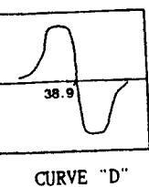
Set the AFT SW to ON position 11. Adjust L203 to place 38.9 MHz marker at reference line on response curve. (Refer to Response Curve "D")
Re-connect CO06, C217 and C218. (solder bridge)
CURVE "R
CURVE "C
ALTENMENT INSTRUCTIONS
SECAM CHROMA BANDPASS ALIGNMENT
TEST EQUIPMENT CONNECTION TEST EQUIPHENT CONNECTION GENERAL ..... PAL-SECAM switch to SECAM position. SWEEP-MARKER GENERATOR ... Connect H. SCOPE and V. SCOPE output cable from SWEEP-MARKEI GENERATOR to H. and V. input GENERATOR to H. and V. input connectors on the OSCILLOSCOPE. connect hot lead of SWEEP-MARKER OUTPUT cable to TP on TV tuner; connect ground lead to chassis ground. Connect pick up lead SWEEP-MARKER INPUT cable to IP604; ground lead to chassis ground.
Adjust L605 to obtain best overall response curve. (Refer to Response Curve "E")


SECAM IDENT ADJUSTMENT
- 1. Receive the signal of secam color pattern. 2. Connect the DC voltmeter to IP603 and ground 3. Adjust the voltage to maximum with L606.
SECAM PHASE ADJUSTMENT
- 1. Receive the signal of secam color pattern. 2. Adjust L601 and L602 not to change the color of the pattern while tuning the Color control from minimum to maximum position.
BLOCK DIAGR

BLOCK DIAGRAM
1-7762
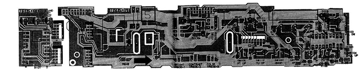
MAIN P.C.BOARD


CRT P.C.BOARD
POWER SW P.C.BOARD

CONTROL/LED P.C.BOARD

NOTE: THIS SCHEMATIC DIAGRAM IS THE I OF PRINTING AND SUBJECT TO CHAN
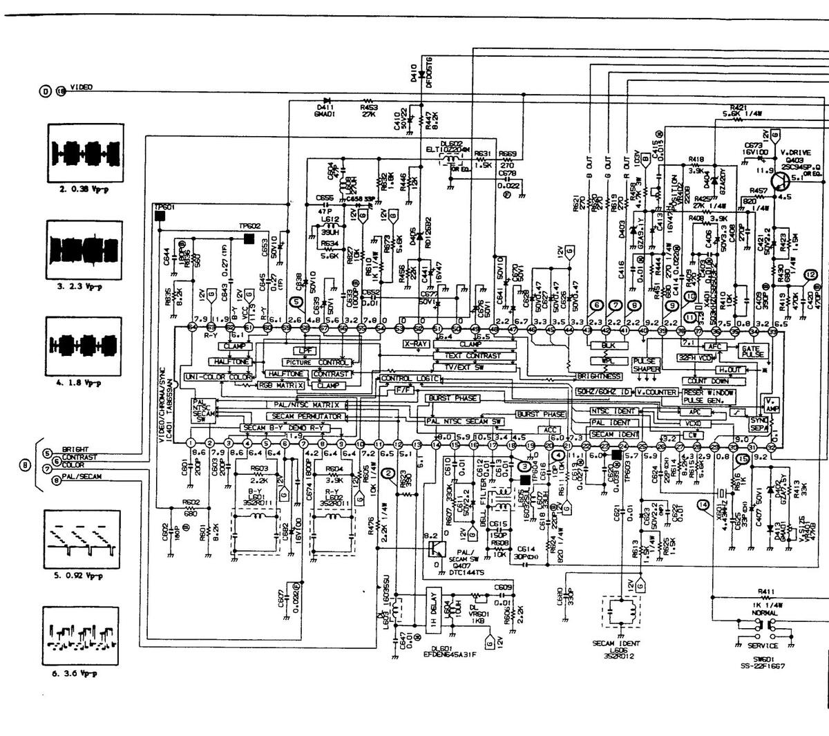
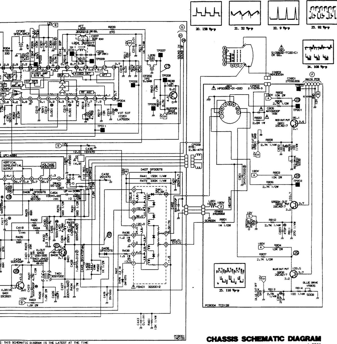
CHASSIS SCHEMATIC DIAGRAM

NOTE: THIS SCHEMATIC DIAGRAM IS THE LATEST AT THE TIME OF PRINTING AND SUBJECT TO CHANGE WITHOUT NOTICE.
CAUTION: DIGITAL TRANSISTOR
TION: DIGITAL TRANSISTOR CHASSIS SCHE
Ł
-₿
٠ĘÌ
CAUTION: SINCE THESE PARTS MARKED BY A ARE CRITICAL FOR SAFETY, USE ONES DESCRIBED ON PARTS LIST ONLY.
ON LES PIECES REPAREES PAR UN Å ETANT DANGEREUSES AN POINT DE VUE SECURITE N'UTILISER QUE CELLES DECRITES DANS LA NOMENCLATURE DES PIECES.
NOTE: THIS SCHEMATIC DIAGRAM IS THE LATEST AT THE TIME OF PRINTING AND SUBJECT TO CHANGE WITHOUT NOTICE,
CHASSIS SCHEMATIC DIAGRAM

1-7719

12
SIS SCHEMATIC DIAGRAM
1-7769

MECHANICAL REPLACEMENT PARTS LIST
| REF.NO | PART NO | DESCRIPTION | |
|---|---|---|---|
|
101
102 103 104 105 106 107 108 109 |
A35473A723
713KPD0016 737KPA0013 735JPA0112 736KPA0003 A35473A743 761JSA0184 751JNA0004 751JNA0008 741JUA0008 |
CABINET, FRONT ASS'Y
DOOR BUTTON, CAP BUTTON, CHANNEL BUTTON, POWER CABINET, BACK ASS'Y SHEET, RATING FRAME, CRT PLATE, EARTH WIRE PLATE, EARTH WIRE SPRING, EARTH |
|
|
111
112 113 |
800JR00003
753KSA0018 749JUA0002 |
SHEET, CRT SUPPORT
EARTH, LUG SPRING, ANTENNA |
|
|
201
202 203 204 |
8117540A82
8110540B04 82A60B2161 8300560004 |
TAPPING(BO) TRUSS
TAP TITE(P) TRUSS WASHER SL NUT |
4*18 BK
4*20 CH 6.3*22*T1.6 M6 |
|
JIAKTGA02A
J3546701A J3546703A J3590128A 792JHA0067 792JHA0068 793JCD1980 |
GUARANTEE CARD
INSTRUCTION BOOK SCHEMATIC DIAGRAM WARNING SHEET PACKAGE,TOP PACKAGE,BOTTOM GIFT BOX |
, |
THIS ELECTRICAL PARTS LIST IS A STANDARD PART LIST, BUT INTERCHANGEABLE PARTS MAY BE USED IN THE UNIT. SEE THE INTERCHANGEABLE PARTS LIST AFTER THE STANDARD PARTS LIST.
ELECTRICAL REPLACEMENT PARTS LIST
| REF.NO | PART NO | DESCRIPTIC | DN . | REF.NO | PART NO | DESCRIPTI | ON | ||
|---|---|---|---|---|---|---|---|---|---|
| -RESISTORS- | -SEMI CONDUCTORS | (CONT) - | |||||||
|
R002
R167 R353 R358 R428 R433 R434 R434 |
R00104152J
R31181123J R31181103J R61582101J R3118A152J R61582680J R5M2CE100J R61481182J |
RC
R.METAL OXIDE R.METAL OXIDE R.FUSE R.METAL OXIDE R.FUSE R.CEMENT R.FUSE |
1.5K OHM 1/4W
12 K OHM 1 W 10 K OHM 1 W 100 OHM 1/2W 1.5K OHM 2 W 68 OHM 1/2W 10 OHM 7 W 1.2 OHM 1 W |
D412
D413 D501 D502 D503 D504 D505 |
D13TGMA010
D13TGMA010 D28020E100 D28020E100 C28020E100 D28020E100 D2800RU2B0 |
DIODE, SILICON
DIODE, SILICON DIODE, SILICON DIODE, SILICON DIODE, SILICON DIODE, SILICON DIODE, SILICON DIODE, SILICON |
GMA-01-BT
GMA-01-BT 20E10 20E10 20E10 20E10 20E1C RU-2B |
||
|
R430
R437 R438 |
R615812R2J
R614811R5J R3128B472J |
R.FUSE
R.FUSE R.METAL OXIDE |
2.2 OHM 1 W
1.5 OHM 1 W 4.7K OHM 3 W |
D506
D508 D511 D512 |
D2BF00RH10
D2B000R2M0 D25T556680 D93T05R10 |
DIODE, RECTIFIER
DIODE, AVARANCHE DIODE, RECTIFIER DIODE, ZENER |
RH-1
R2M S5566B GZA5.1 Y BT |
||
| ▲ |
R463
R501 R506 R509 R514 R802 R803 R804 R804 R820 |
R3118A152J
R5M2CD5R6K R3118A220J R31181103J R31181103J R31181103J R3118A103J R3118A103J R3118A103J R3118A103J R3118A103J |
R.METAL OXIDE
R.CEMENT R.METAL OXIDE R.METAL OXIDE R.METAL OXIDE RC R.METAL OXIDE R.METAL OXIDE R.METAL OXIDE RC |
1.5K OHM 2 W
5.6 OHM 5 W 22 OHM 2 W 10K OHM 1 W 5.6K OHM 1 W 5.6K OHM 1/6W 10K OHM 2 W 10K OHM 2 W 10K OHM 2 W 2.2M OHM 1 W |
| C101
| C102 | C103 | C104 | C105 | C106 | C107 | C108 | C201 | C401 |
IC1D10B210
I30S1006LC I51D080246 I019012805 I03S079100 I03D063581 I02190574 I02190574 I02A98L050 I03DE75200 I03DE75200 |
AN90B21
CXK1006L QEC8024B MN1280S LA7910 LA6358T UPC574J-T UPC78L05 LA7520N TA8659AN |
||
| -CAPACITURS- | 1200 BE 50V | • | 10402 | 102SD14880 | UPC1488H | ||||
|
C134
C356 C425 C427 C428 C429 C429 C430 C431 C449 C452 |
COKOBO4B3K
E085FB220M P441F2824J P441F2864J P442F9123J E087F4102M E087F3222M E085FD4R7M C018B0702K E085FB101M |
СС
СЕ СМРР СМРР СМРР СЕ СЕ СЕ СЕ СС СС СС |
1200 PF 50v 22 UF 160v 0.82 UF 200v 0.56 UF 200v 0.012 UF160v 1000 1000 UF 35v 2200 UF 25v 4.7 UF 25v | ₿ |
Q102
Q103 Q104 Q105 Q104 Q105 Q106 Q107 Q111 Q112 |
12E4901034
TA2T009522 TA2T009522 TC2T00952 TC2T009450 TN7TD03002 TC2T009450 TP7TD03002 TN7TD03000 |
IC
IC TRANSISTOR,SILICON TRANSISTOR,SILICON TRANSISTOR,SILICON COMPOUND,TRANSISTOR COMPOUND,TRANSISTOR COMPOUND,TRANSISTOR COMPOUND,TRANSISTOR |
STRS0103A
2SA952-T 2SA952-T 2SA952-T 2SC945-T (IC) DTC144TS 2SC945-T (IC) DTC144TS (IC) DTC144ESTP |
|
| C502 | E0260H101T | CE |
100 UF 400V
0.0022UF 2KV |
в |
Q115
Q116 |
TC2T009450
TN7TD03002 |
TRANSISTOR, SILICON
COMPOUND, TRANSISTOR |
2SC945-T
R(IC) DTC144TS |
|
| ≵ |
C509
C511 C513 C514 C515 C516 C518 C518 C673 |
C02FB07H3K
C02FB07H3K P4440B474M P4440B104M C03BBN7W2K C01BB07N2K C01BBN713K E0B7T2101M |
CC
CC CMPP CMPP CC CC CC CC CC |
0.0022UF 2KV
0.0022UF 2KV 0.47 UF 250V 0.1 UF 250V 820 PF 2KV 390 PF 2KV 0.001 UF 2KV 100 UF 16V |
B
B B B |
Q117
Q201 Q351 Q352 Q401 Q402 Q403 Q404 |
TN7TD03002
TC3T030002 TC30041590 TC30041590 TC30041590 TC30026211 TD5F015550 TC2T009450 TC2T009450 |
COMPOUND, TRANSISTOR
TRANSISTOR, SILICON TRANSISTOR, SILICON TRANSISTOR, SILICON TRANSISTOR, SILICON TRANSISTOR, SILICON TRANSISTOR, SILICON TRANSISTOR, SILICON |
1(1C) DTC144TS
2SC3000-AA 2SC4159 2SC4159 2SC2621E-RAC 2SD1555 2SC945-T 2SC945-T 2SC945-T |
| ▲ |
C674
C678 C801 C805 |
COBOBO4G3K
COBOF04H4Z CO2FB07H3K CO3FE09H3M |
0.00180F 50V
0.022 UF 50V 0.0022UF 2KV 2200 PF 4KV |
Y
Z B E |
Q405
Q406 |
TC2T009450 |
TRANSISTOR, STLICON
TRANSISTOR, SILICON |
250945-T
250945-T |
|
| -SEMICONDUCTORS- |
Q517
Q504 |
TC3T02909 | TRANSISTOR, SILICON |
25C29095
25A733-T |
|||||
|
D101
D102 D103 D104 D105 |
0040322001
0021121050 0021121050 0021121050 0021121050 D13TGMA010 |
LED DISPLAY IC
LED LED LED DIODE-SILICON |
SL-1263H
LN81RCPH-(C) LN81RCPH-(C) LN81RCPH-(C) GMA-01-BT |
Q801
Q802 Q803 |
TC3F042170
TC3F042170 TC3F042170 |
TRANSISTOR.SILICON
TRANSISTOR.SILICON TRANSISTOR.SILICON - COILS & TRANSF |
2SC4217-RAC
2SC4217-RAC 2SC4217-RAC 2SC4217-RAC |
||
|
D106
D108 D109 D110 D111 |
D13TGMA010
0021121050 0021121050 0021121050 0021121050 0021121050 |
LN81RCPH-(C)
LN81RCPH-(C) LN81RCPH-(C) LN81RCPH-(C) LN81RCPH-(C) |
L001
L202 L203 L204 L205 |
021JA6100
021JA61R0 033600016 033600017 021JA6100 |
COIL LALO2TA100K
COIL EL0606RA-1ROM COIL.VIDEO IFT COIL.VIDEO IFT COIL LALO2TA100K |
10 UH
1.0 UH 3600016 3600017 10 UH |
|||
|
D112
D113 D114 D115 D117 |
D13TGMA010
D13TGMA010 D13TGMA010 D13TGMA010 D13TGMA010 D13TGMA010 |
DIODE, SILICON
DIODE, SILICON DIODE, SILICON DIODE, SILICON DIODE, SILICON |
GMA-01-BT
GMA-01-BT GMA-01-BT GMA-01-BT GMA-01-BT GMA-01-BT |
L206
L207 L301 L401 L402 |
0336000180
03360M0010 021JA61501 0216794721 0221000004 |
COIL.VIDEO IFT
COIL.TRAP COIL LALO2TA150K COIL EL0909RR-472K COIL.LINEARITY |
3603018
360M301 15 UH 4.7 MH 21000004 1450MS |
||
|
D122
D123 D124 D136 D139 |
D137GMAD10
D137GMA010 D137GMA010 D2575566B0 D137DS442X |
DIODE.SILICON
DIODE.SILICON DIODE.SILICON DIODE.RECTIFIER DIODE.SILICON |
GMA-01-BT
GMA-01-BT S5566B DS442X-BT |
₥ |
L501
L502 L503 L601 L602 |
029100000
028Y20000 02AXA509C 03352R0110 03352R0110 |
2 COIL,LINE FILTER
3 COIL,DEGAUSS FILTER,LINE 5 COIL,CHROMA 5 COIL,CHROMA |
91000002
8Y200008 ESD-R-16C 352R011 352R011 |
|
|
D351
D352 D401 D402 D403 |
D13TGMA010
D13TGMA010 D13TGMA010 D13TGMA010 D93T07R50Y D93T09R10Y |
DIODE, SILICON
DIODE, SILICON DIODE, SILICON DIODE, ZENER DIODE, ZENER |
GMA-01-BT
GMA-01-BT GMA-01-BT GZA7.5 Y BT GZA9.1 Y BT GZA9.1 Y BT |
L603
L604 L605 L606 L607 |
03352R007(
021JA6100) 03302R001( 03352R012) 021JA6330| |
G COIL, CHROMA
COIL LALOZTA100K COIL, CHROMA G COIL, CHROMA COIL LALOZTA330K |
1603550
10 UH 302R001 1603250 352R012 33 UH |
||
|
0404
D405 D406 D407 |
D93102000
D92T0120B2 D23TFD05TG D23TFD05TG |
DIODE,ZENER
DIODE,RECTIFIER DIODE,RECTIFIER DIODE,RECTIFIER |
RD12EB 2 TA11R
DFD05TG-BT DFD05TG-BT DFH10TG-KB4 |
L608
L612 L801 |
021JA62701
021JA63901 021JA21511 |
COIL LALC2TA270K
COIL LALC2TA390K COIL LALC3TA151K |
27 UH
39 UH 150 UH |
||
|
D408
D409 D410 D411 |
D23FFH1010
D23FFH1010 D23FFD05T0 D13FGMA010 |
DIODE.RECTIFIER
DIODE.RECTIFIER DIODE.SILICON |
DFH10TG-KB4
DFD05TG-BT GMA-01-BT |
≵ |
T101
T351 T401 |
040835013
045128007 03305Y002 |
TRANSFORMER POWER A
TRANSSOUND OUTPUT TRANSHORIZONTAL D |
AC 0835013
5128007 DRIVE 305Y002 |
| DESCRIPTION | REF.NO PART NO DESCRIPTION | ON | ||||||||
|---|---|---|---|---|---|---|---|---|---|---|
| 345 T NO | PARINU | - COILS & TRANSFO | RMERS (CONT)- | -MISCELLANEOUS (CONT)- | ||||||
| -501 | 0481330107 |
TRANSFORMER.SWITCHIN
- JACKS- |
NG 8133010T |
DL 602
EAR351 |
103S000402
074U130009 0808T2R502 |
DELAY LINE
EARPHONE FUSE |
ELT10Z204M
4U130009 T 2.5A 250V |
|||
| L |
- 8* 1
. * 5* |
0602101004 |
JACK.RCA 3.5
SOCKET.CRT |
HSJ0912-01-050
HPS0360-01-020 |
Δ |
FH501
FH502 MS002 |
0432200121
067M0T0004 067M0T0005 128B000017 |
HOLDER, FUSE
HOLDER, FUSE MICA, SHEET |
5220012
H0451 H0452 STR-50103MICA |
|
| 1.4 | -SWITCHES- |
NR101
05101 |
077M006004 | REMOTE RECIVER | KEY-C00SV2 | |||||
|
50-192
50-192 50-193 50-193 50-193 50-199 50-199 50-19 50-19 50-19 |
0501201007
0504101T13 0504101T13 0504101T13 0504101T13 0504101T13 0504101T13 0504101T13 0504101T13 0504101T13 0504101T13 |
SWITCH, PUSH
SWITCH, TACT SWITCH, TACT SWITCH, TACT SWITCH, TACT SWITCH, TACT SWITCH, TACT SWITCH, TACT SWITCH, TACT SWITCH, TACT |
SPPH 1 1280A
EVG-GTN090 EVG-GTN090 EVG-GTN090 EVG-GTN090 EVG-GTN090 EVG-GTN090 EVG-GTN090 EVG-GTN090 EVG-GTN090 |
瓫 |
S001
SP351 TH501 TM101 TU001 V801 X401 X401 X601 |
128F100003
070B043001 D810M180H0 076M027001 0145P11004 098F200410 1002R50301 10064R43B2 |
SPACER
SPEAKER DEGAUSS ELEMENT TRANSMITTER TUNER,UHF-VHF TUBE,CATHODE RAY CERAMIC OSCILLATOR CRYSTAL HC-49/U |
BUSH-M
C100A21K2453 ERP-F5B0M180H R-56 5710 VTSA1SZV 5109B22-TC20(C) CSB503F2 4.43361875MHZ |
||
| t. |
0504101T13
0504101T13 0510822001 0530102008 0510822001 |
SWITCH, TACT
SWITCH, TACT SWITCH, SLIDE SWITCH, PUSH SWITCH, SLIDE |
EVQ-QTN09Q
EVQ-QTN09Q SS-22F16G7 ESB-76937A SS-22F16G7 |
|||||||
| -VARIABLE RESISTO | DRS- | |||||||||
|
55 54
55251 55452 55452 55452 55452 55452 55452 55452 55 55252 55252 55252 |
V115213B03
V116303B02 V116304B03 V1163H2B02 V1263L5B01 V1263L5B01 V029300007 V176553B01 V176558D01 V17553B02 |
VR.SEMIFIXED EX VR.SEMIFIXED RX |
/N-K0AA00B13
/N-D4AA00BQ3 /N-D4AA00BQ4 /N-D4AA00BE2 10615CN5J0F /N-D4AA00B13 (09Z3330012 /A0911H304-1-501M /A0911H304-1-501M /A0911H304-2-502M |
|||||||
|
1512/1
1512/1 1512/121 |
v175C53803
v175C52803 |
VR.SEMIFIXED RI
VR.SEMIFIXED RI |
/A0911H304-3-502M
/A0911H304-3-501M |
l | ||||||
| -P.C. BOARDS ASS'Y- | ||||||||||
|
۲۰٫۲۵۲٫۰۱
۲۰٫۲۵۲٫۰۶ ۲۰٫۲۵۲٫۰۵ ۲۰٫۲۵۲٬۰۰۰ ۲۰٫۲۵۲٬۰۲ |
A35473A01A5
A36473A03A A36473A20A A36473A11A A36473A38A |
S PCB ASS'Y
PCB ASS'Y PCB ASS'Y PCB ASS'Y PCB ASS'Y PCB ASS'Y |
TM0155-5
TE0517 TE0518 TC0128 TE0357 |
|||||||
| -MISCELLANEOUS- | ||||||||||
| h. |
0637300013
024JT03551 024JT03551 141T004003 141T004003 068032001A 068012183A 0694260080 0694260080 |
ANT.UNIT
CORE,BEADS CORE,BEADS BATTERY,MANGAN BATTERY,MANGAN CORD EIS CONNECTOR CORD JUMPER CONNECTOR PCB SIDE CONNECTOR PCB SIDE |
ATCU-PS-26
FBA04HA450AB-00 FBA04HA450AB-00 UM-4 UM-4 8G32001A 8M12183A 174074-6 174074-6 |
|||||||
| ŀ. |
122N091001
122N091001 0694290080 068001173A 068001173A 1227055306 1227035302 668643002A 116F3TH4Z1 |
CORD, JUMPER
CORD, JUMPER CONNECTOR PCB SIDE CORD, AC CORD CONNECTOR CORD CONNECTOR CORD, JUMPER CORD, JUMPER CORD, JUMPER CORD UX CONNECTOR FILTER, EMI |
2N091001
2N091001 174074-9 120$450024 8601173A 8601174A 27055306 27035302 8643002A LTSTF223ZBTB |
|||||||
| · |
116F3TH4Z1
116F3TH4Z1 116F3TH4Z1 1003T4R001 1027038R91 1012105R51 101225R501 1012005R52 116F3TH4Z1 649Z320018 |
FILTER,EMI
FILTER,EMI CERAMIC OSCILLATOR FILTER,SAW FILTER,CERAMIC TRAP FILTER,CERAMIC FILTER,CERAMIC FILTER,EMI CONNECTOR PCB SIDE |
LTSTF223ZBTB
LTSTF223ZBTB KBR-4.0MSTF F1034 TPS5.5MB CDA5.5MC24B SFE5.5MC2 LTSTF223ZBTB RTB-2.36-2TV |
RESISTOR
RCCARBON RESISTOR CAPACITORS CCALUMI ELECTROLYTIC CAPACITOR CPPOLYESTER CAPACITOR CPPPOLYERTER CAPACITOR CPLMETAL POLYESTER CAPACITOR CMPLMETAL POLYESTER CAPACITOR CMPPMETAL POLYESTER CAPACITOR CMPPMETAL POLYENER CAPACITOR CMPPMETAL POLYENER CAPACITOR |
N RESISTOR
IC CAPACITOR ELECTROLYTIC CAPACI STER CAPACITOR ROPYLENE CAPACITOR IC CAPACITOR |
TOR | ||||
|
5692340018
5694260090 5694260090 5694290260 5694290260 5694430100 104114R436 |
CONNECTOR PCB SIDE
CONNECTOR PCB SIDE CONNECTOR PCB SIDE CONNECTOR PCB SIDE CONNECTOR PCB SIDE CORD UX CONNECTOR DELAY LINE GLASS |
RTB-2.36-4TV
174161-6 174161-6 175544-9 0692420039 2-173270-3 EFDEN645A31F |
TOR | |||||||
INTERCHANGERABLE PARTS LIST
NOTE: THE FOLLOWING PART(S) MAY BE SUBSTITUTED FOR PARTS INDICATED IN THE BASIC PART(S) LIST (WITH THE SAME REF.NO.). THESE PARTS SHARE THE SAME ELECTRICAL CHARACTERISTICS AND OTHER ELEMENTS FOR COMMON USAGE. EITHER PART NUMBER MAY BE USED IN THIS UNIT.
| REF.NO | (PART NO.) | (PART NO.) |
|---|---|---|
| Q105 | 2SC945-T | 25C945A(C)-T |
| (1021009450) | ||
| Q107 | 250945-1 | 2309454(0)-1 |
| (1021009450) | 25C9454(C) -T | |
| Q115 | 230943-1 | |
| 250045-7 | 25C9454(C) -T | |
| 0403 | 230345-1 | (TCL T009450) |
| 1 202 | 3600016 | 3600016 |
| 1203 | (033600016N) | (033600016G) |
| 1 204 | 3600017 | 3600017 |
| 1204 | (033600017N) | (033600017G) |
| 1 206 | 3600018 | 3600018 |
| 200 | (0336000186) | (033600018N) |
| 1 207 | 360M001 | 360M001 |
| (03360M001G) | (03360M001N) | |
| T101 | 0835013 | 0835013 |
| (040835013Z) | (040835013P) | |
| T501 | 8133010T | 8133010 |
| (048133101T) | (0481330105) | |
| BT101 | UM-4 | RO3(UM-4(SP)) |
| (141T004003) | (1412004002) | |
| BT102 | UM-4 | R03 (UM-4 (SP)) |
| (141T004003) | (1412004002) | |
| CF101 | KBR-4.0MSTF | KBR-4.0M |
| (1003T4R001) | (10034R0001) | |
| DL 602 | ELT10Z204M | ELT10Z204M |
| (1035000402) | (1031000402) | |
| FH501 | H0451 | 773JEE0004 |
| (067M0T0004) | (06/H000003) | |
| FH502 | H0452 | (/3JEE0004 |
| (067M010005) | ||
| TU001 | VISAISZV |
VISAIS2V
(0145 111004) |
| (0145P11004) | E10VUP32-TC1 | |
| V801 | 5109B22-1C20 | |
| (098+200410) | 103062004107 |
.


 Loading...