

Page 1
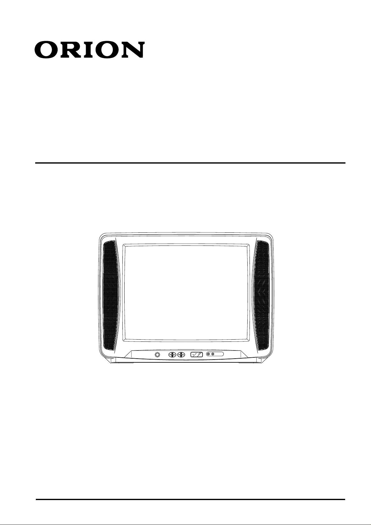
21MT9A
SERVICE MANUAL
COLOR TELEVISION RECEIVER
ORIGINAL
MFR’S VERSION B
Design and specifications are subject to change without notice.
Page 2
SERVICING NOTICES ON CHECKING
As for the places which need special attentions,
they are indicated with the labels or seals on the
cabinet, chassis and parts. Make sure to keep the
indications and notices in the operation manual.
2. AVOID AN ELECTRIC SHOCK
There is a high voltage part inside. Avoid an
electric shock while the electric current is flowing.
3. USE THE DESIGNATED PARTS
The parts in this equipment have the specific
characters of incombustibility and withstand
voltage for safety. Therefore, the part which is
replaced should be used the part which has the
same character.
Especially as to the important parts for safety
which is indicated in the circuit diagram or the
table of parts as a mark, the designated parts
must be used.
4. PUT PARTS AND WIRES IN THE
ORIGINAL POSITION AFTER
ASSEMBLING OR WIRING
There are parts which use the insulation material
such as a tube or tape for safety, or which are
assembled in the condition that these do not
contact with the printed board. The inside wiring is
designed not to get closer to the pyrogenic parts
and high voltage parts. Therefore, put these parts
in the original positions.
5. TAKE CARE TO DEAL WITH THE
CATHODE-RAY TUBE
In the condition that an explosion-proof cathoderay tube is set in this equipment, safety is secured
against implosion. However, when removing it or
serving from backward, it is dangerous to give a
shock. Take enough care to deal with it.
6. AVOID AN X-RAY1. KEEP THE NOTICES
Safety is secured against an X-ray by considering about the cathode-ray tube and the high
voltage peripheral circuit, etc.
Therefore, when repairing the high voltage peripheral circuit, use the designated parts and
make sure not modify the circuit.
Repairing except indicates causes rising of high
voltage, and it emits an X-ray from the cathoderay tube.
7. PERFORM A SAFETY CHECK AFTER
SERVICING
Confirm that the screws, parts and wiring which
were removed in order to service are put in the
original positions, or whether there are the
portions which are deteriorated around the
serviced places serviced or not. Check the
insulation between the antenna terminal or
external metal and the AC cord plug blades.
And be sure the safety of that.
(INSULATION CHECK PROCEDURE)
1.
Unplug the plug from the AC outlet.
2.
Remove the antenna terminal on TV and turn
on the TV.
3.
Insulation resistance between the cord plug
terminals and the eternal exposure metal
[Note 2] should be more than 1M ohm by
using the 500V insulation resistance meter
[Note 1].
4.
If the insulation resistance is less than 1M
ohm, the inspection repair should be
required.
[Note 1]
If you have not the 500V insulation
resistance meter, use a Tester.
[Note 2]
External exposure metal: Antenna terminal
HOW TO ORDER PARTS
Please include the following informations when you order parts. (Particularly the VERSION LETTER.)
1. MODEL NUMBER and VERSION LETTER
The MODEL NUMBER can be found on the back of each product and the VERSION LETTER can be
found at the end of the SERIAL NUMBER.
2. PART NO. and DESCRIPTION
You can find it in your SERVICE MANUAL.
IMPORTANT
Inferior silicon grease can damage IC's and transistors.
When replacing an IC's or transistors, use only specified silicon grease (YG6260M).
Remove all old silicon before applying new silicon.
TO CANCEL HOTEL LOCK
• Hotel lock can be cancelled by following steps 1-2.
1.
Press and hold the CHANNEL UP button on the TV, and press the POWER button on the remote
control simultaneously.
2.
Press the SET +/– button to select the HOTEL LOCK ALL CLEAR mode, then press the ENTER button.
The "OK" indicator appears for 4 seconds on the screen.
A1-1
Page 3

CONTENTS
SERVICING NOTICES ON CHECKING......................................................................................................
HOW TO ORDER PARTS ...........................................................................................................................
IMPORTANT................................................................................................................................................
TO CANCEL HOTEL LOCK........................................................................................................................
CONTENTS .................................................................................................................................................
GENERAL SPECIFICATIONS ....................................................................................................................
DISASSEMBLY INSTRUCTIONS
1. REMOVAL OF ANODE CAP ..............................................................................................................
2. REMOVAL AND INSTALLATION OF FLAT PACKAGE IC ................................................................
SERVICE MODE LIST.................................................................................................................................
CONFIRMATION OF USING HOURS.........................................................................................................
NOTE FOR THE REPLACING OF MEMORY IC ........................................................................................
ELECTRICAL ADJUSTMENTS ..................................................................................................................
MAJOR COMPONENTS LOCATION GUIDE .............................................................................................
BLOCK DIAGRAM ......................................................................................................................................
PRINTED CIRCUIT BOARDS
MAIN/CRT..........................................................................................................................................
T' TEXT/FRONT AV JACK ................................................................................................................
SCHEMATIC DIAGRAMS
MICON/TUNER..................................................................................................................................
IF/CHROMA/SOUND AMP ................................................................................................................
SOUND ..............................................................................................................................................
POWER .............................................................................................................................................
DEFLECTION/CRT............................................................................................................................
JACK..................................................................................................................................................
VIDEO/R.G.B SWITCH......................................................................................................................
FRONT AV JACK...............................................................................................................................
T' TEXT ..............................................................................................................................................
WAVEFORMS .............................................................................................................................................
MECHANICAL EXPLODED VIEW ..............................................................................................................
MECHANICAL REPLACEMENT PARTS LIST ..........................................................................................
ELECTRICAL REPLACEMENT PARTS LIST ............................................................................................
A1-1
A1-1
A1-1
A1-1
A2-1
A3-1~A3-4
B-1
B-2, B-3
C-1
C-1
C-1
D1-1~D2-1
D3-1
E-1, E-2
F-1~F-4
F-5, F-6
G-1, G-2
G-3, G-4
G-5, G6
G-7, G-8
G-9, G-10
G-11, G-12
G-13, G-14
G-15, G-16
G-17, G-18
H-1, H-2
I-1
J1-1
J2-1, J2-2
A2-1
Page 4
GENERAL SPECIFICATIONS
G-1.Ou tline of the P roduct
21 inch(544.5
Color CRT 90 degree deflection
G-2.Broadcasting System
CCIR System B/G
G-3.Color System NTSC PAL SECAM or Monochrome signal
mmV):Measured diagonally
G-4.NTS C Playb ack(PAL 60Hz)
G-5.NTSC 3.58+4 .43/PAL60Hz
G-6.An tenna Input Impedance
VHF/UHF 75 ohm unbalanced
G-7.Tuner and Receiving
Tuner : Contactless Electric Tuner
Oscar(W/O HYPER) Oscar(W/ HYPER) Fr an c e CATV) Others
channel coverag e
(PAL) AUS0 , E2 ~ E4
S11 ~ S41 , E21 ~ E69
Tuning System
Frequency syn. Voltage syn. Others
G-8.Preset Channel
110 channels
G-9.Intermediate Frequency
Picture(fP) 38.90 MHz
Sound (fS) 34.47 MHz MHz MHz
fP-fS 33.40 MHz MHz MHz
G-10.Stereo/D ual TV Sound
Yes( NICAM GERMAN USA JAPAN) No
G-11.Tuner Sound Muting
G-12.Power Source 240 V
Yes No
Yes No
Yes No
, X ~ Z+2 , S1 ~ S10 , E5 ~ E12 ,
MHz MHz
AC 50Hz AC 60Hz
G-13.Power Consumption: 50 W at AC 240 V 50 Hz
-- W at DC --- V
Stand by: 10 W at AC 240 V 50 Hz
Per Year: -- kWh / Year
G-14.Dimensions(Approx.)
600 mm(W) 480
G-15.Weight(Approx.) Net : 20.7 kg ( -- lbs)
Gross: 23.5 kg ( -- lbs)
G-16.Cabinet Material
Cabinet Front:
Back Panel:
mm(D) 446 mm(H)
PS 94HB DECABROM
ABS 94V2 NON-DECA
94V0
PS 94HB DECABROM
ABS 94V2 NON-DECA
94V0
A3-1
Page 5

GENERAL SPECIFICATIONS
G-17.Protector: Power Fuse
G-18.Regulation
Safety
UL CSA SAA SI CE SEV
BS NF NEMKO FEMKO DEMKO IEC65
SEMKO NZ HOMOLO SABS CNS SISIR
NOM AS3159 DENTORI UNE GOST NONE
Radiation
FCC DOC FTZ PTT CE SEV
SABA SI NF NZ HOMOLO UNE
CNS CISPR13 DENTORI AS/NZS NONE
X-Radiation
PTB DHHS HWC DENTORI NONE
G-19.Temperature
Operation 5 ºC~ 40
Storage -20 ºC~ 60 ºC
G-20.Operating Humidity Less than 80 %RH
G-21.Clock an d Timer
Sleep Timer
On/Of f Ti mer Yes 4 Programs No
Wake Up T imer Yes Programs No
G-22.Timer back up Time
More than -- Minutes (at Power Off Mode)
G-23.Terminals
VHF/UHF Ante n na Inpu t Din Type F-Type France Type
Front Video Input (RCA ø8.3)
Front Audi o Input (RCA ø8 .3)
Rear Video Input (R CA ø8 .3)
Rear Audio Input (RCA ø8.3)
Rear Video Output (RCA ø8.3)
Rear Audio Output (RCA ø8.3)
21 Pin (x ) DC Jack(Center +) E ar Phon e Jack(ø3.5)
Head Phone(Stereo & Mono) AC Outle t Ext Speaker
Diversity S Input(Front) S Input(Rear)
G-24.Indicator
Power Stand By On Timer NONE
( ) (Red) ( )
G-25.Display
On Screen Display
Menu Clock Set( 12H 24H) System Selec On/Off T im er
Hotel L ock Area Cod e CH Tuning
Sound 1/2 NICAM Au to Off Picture
Guide CH Set Audio Language
CATV Pin Code Registration
Control Level Sound Brightness Contrast
Color Tint(NTSC Only) Sharpness
Tuning Bass Treble
Balance Back Light
Stereo,Audio Output,Bilingual Picture Menu
Stereo,Aud io Out pu t,SAP Mid Night Theater
Stereo,Aud io Out pu t GAME
CH/AV Clock Pin Code Ho tel L ock
Sleep Timer Sound Mute Channel Band
PAL/NTSC3.58/NTSC4.43 AFT Video
ºC
Yes Max 120 Min.( 10 Min. Step) No
A3-2
Page 6
GENERAL SPECIFICATIONS
G-26.OSD Language
Eng Ger Fre Spa Ita Por Jpn
OSD Language Setting
Eng Ger Fre Spa Ita Por Jpn
Not Appl icable
G-27.Speaker
Pos ition
Size 6 1/4 x 2 1/4 inches
Imp. 4 ohm x 2 pcs
Power Max 1.25 + 1.25 W
10% 1.0 + 1.0 W (Typical)
G-28.EX T Speaker : Yes -- W Imp -- ohm
G-29.Carton
Master Carton:
Gift Box
Drop Test Natural Dropping At 1 Corner / 3 Edges / 6 Surfaces
Container Stuffing: 304 Sets / 40' container
G-30.Accessories
Content: ---- Set
Material: ---- / ---- Corrugated Carton
Dimensions: ---- mm(W) ---- mm(D) ---- mm(H)
Description of Origin Yes No
Material
Dimensions: 660 mm(W) 540
Design: As Per BUYER 's
Description of Origin: Yes No
Owner's Manual ( W/Guarantee Card) [English]
AC Plug Adapter Channel Film
Battery (UM- 4 x 2 ) Remote Control Unit
Safety Tip Toll Free Insert Sheet
Guarantee Card Audio-Video Cord (RCA)
Regist ra tio n Card Warning Sheet
Quick Se t-Up Sheet Schematic Diagram
Information Sheet U/V Mixer
75 ohm Coaxial Cable ( Single Shield Double Shield)
300 ohm to 75 ohm VHF Antenna Adaptor
21pin Cable Car Cord
Rod Ant enn a
One Pole Two Pole ( F-Type Din Type France Type)
Loop Antenna ( F-Type Din Type France Type)
Need No Need
Double/Brown Corrugated Carton ( with Ph oto Label )
Double/White Corrugated Carton ( with Photo Label)
Double Full Color Carton W/Photo
Height
Front Side Bottom
mm(D) 541 mm(H)
25cm 31cm 46cm 62cm 80cm
G-31.Other Features
Auto Degauss Auto Search Full OS D
Auto Shut Off CH Allocation Premiere
Canal+ SAP Comb Filter
CATV Channel Lock Auto CH Memory
Anti-Theft Just Clock Function Hote l Lock
Rental Game Position Fastext
Unitext TopText Closed Caption
Picture Menu Mid Night Theater
Memory( Last Ch Last Vol.)
A3-3
Page 7
GENERAL SPECIFICATIONS
G-32.Switch
Front
Power(Tact) Channel Up Volume Up
System Select Channel Down Volume Down
Main Power SW Sub Power
Rear
AC/DC TV/CATV Selector
Degauss Main Power SW
G-33.Magnetic Fiel d
BV : +0.45G BV : +0.35G BV : +0.25G
BH : 0.18G BH : 0.30G BH : 0.30G
BV : -0.15G BV : -0.25G BV : -0.50G
BH : 0.15G BH : 0.15G BH : 0.30G
G-34.Remote Control Unit: RC-BQ
Glow in Dark Remocon Yes No
Power Source: D.C 3 V Battery UM - 4 x 2
Total : 38 Key
Power Quick View TV/AV
Stand By Status Bar Select
0/AV Time Select PAL/SECAM
1 Time Set Volume Up
2 Mute Volume Down
3 CH Skip CH Call
4 CH1/CH2 C H Down
5 Channel CH Up
6 Text/Mix/TV CH Down /Page Down
7 Display Cancel CH Up/Page Up
8 Initial Page +/ 9 Store Program
10 Reveal F/T/B
11 Sleep Hold
12 Skip List
1 * Preset Rotate
2 * 5.5/6.5MHz Browse
0/10 Auto Memo ry Std/Auto
Tone 1/2 Auto Memory
Info Call Band Select
Mono/Auto Reset Search
TV/Caption/Text Menu Clock/Program
Expand Enter Clock/Set
Red Add Ch Set
Cyan Delete Set +
Normal Yellow Set Color Syst em Ra nd om Green
Wide Selecy Tuning Up/Time Text Nicam/Mono
Auto Wi de On/Off Tuning Down/Reset Tone A/B
Picture Position Navi FM Transm i tter
Direct Change/Auto Search Ba ck L ig ht
Picture Menu Mid Night Theate r ./ ..
A3-4
Page 8
DISASSEMBLY INSTRUCTIONS
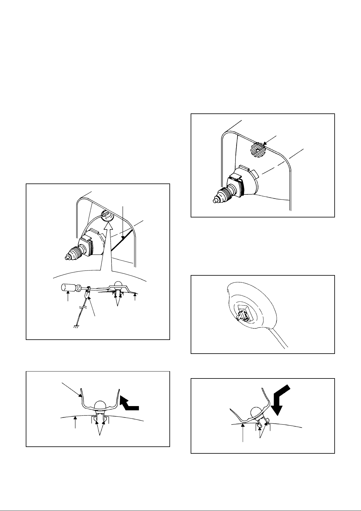
1. REMOVAL OF ANODE CAP
Read the following NOTED items before starting work.
*
After turning the power off there might still be a potential
voltage that is very dangerous. When removing the
Anode Cap, make sure to discharge the Anode Cap's
potential voltage.
*
Do not use pliers to loosen or tighten the Anode Cap
terminal, this may cause the spring to be damaged.
REMOVAL
1. Follow the steps as follows to discharge the Anode Cap.
(Refer to Fig. 1-1.)
Connect one end of an Alligator Clip to the metal part of a
flat-blade screwdriver and the other end to ground.
While holding the plastic part of the insulated Screwdriver,
touch the support of the Anode with the tip of the
Screwdriver.
A cracking noise will be heard as the voltage is discharged.
GND on the CRT
3. After one side is removed, pull in the opposite direction to
remove the other.
NOTE
Take care not to damage the Rubber Cap.
INSTALLATION
1. Clean the spot where the cap was located with a small
amount of alcohol. (Refer to Fig. 1-3.)
Location of Anode Cap
Fig. 1-3
NOTE
Confirm that there is no dirt, dust, etc. at the spot where
the cap was located.
2.3.Arrange the wire of the Anode Cap and make sure the
wire is not twisted.
Turn over the Rubber Cap. (Refer to Fig. 1-4.)
Screwdriver
Alligator Clip
GND on the CRT
Flip up the sides of the Rubber Cap in the direction of the
2.
arrow and remove one side of the support.
(Refer to Fig. 1-2.)
Rubber Cap
CRT
Support
Support
CRT
Fig. 1-1
Fig. 1-2
Fig. 1-4
4. Insert one end of the Anode Support into the anode button,
then the other as shown in Fig. 1-5.
Support
CRT
5.6.Confirm that the Support is securely connected.
Put on the Rubber Cap without moving any parts.
Fig. 1-5
B-1
Page 9
DISASSEMBLY INSTRUCTIONS
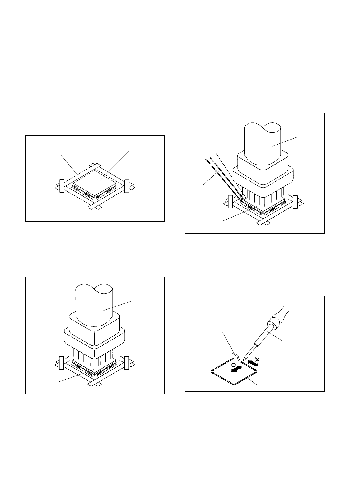
2.
REMOVAL AND INSTALLATION OF
FLAT PACKAGE IC
REMOVAL
Put the Masking Tape (cotton tape) around the Flat
1.
Package IC to protect other parts from any damage.
(Refer to Fig. 2-1.)
NOTE
Masking is carried out on all the parts located within
10 mm distance from IC leads.
When IC starts moving back and forth easily after
3.
desoldering completely, pickup the corner of the IC using
a tweezers and remove the IC by moving with the IC
desoldering machine. (Refer to Fig. 2-3.)
NOTE
Some ICs on the PCB are affixed with glue, so be
careful not to break or damage the foil of each IC
leads or solder lands under the IC when removing it.
Blower type IC
desoldering
machine
Masking Tape
(Cotton Tape)
Heat the IC leads using a blower type IC desoldering
2.
IC
machine. (Refer to Fig. 2-2.)
NOTE
Do not add the rotating and the back and forth
directions force on the IC, until IC can move back and
forth easily after desoldering the IC leads completely.
Blower type IC
desoldering machine
Fig. 2-1
Tweezers
IC
Fig. 2-3
Peel off the Masking Tape.4.
Absorb the solder left on the pattern using the Braided
5.
Shield Wire. (Refer to Fig. 2-4.)
NOTE
Do not move the Braided Shield Wire in the vertical
direction towards the IC pattern.
Braided Shield Wire
Soldering Iron
IC
Fig. 2-2
IC pattern
Fig. 2-4
B-2
Page 10
DISASSEMBLY INSTRUCTIONS
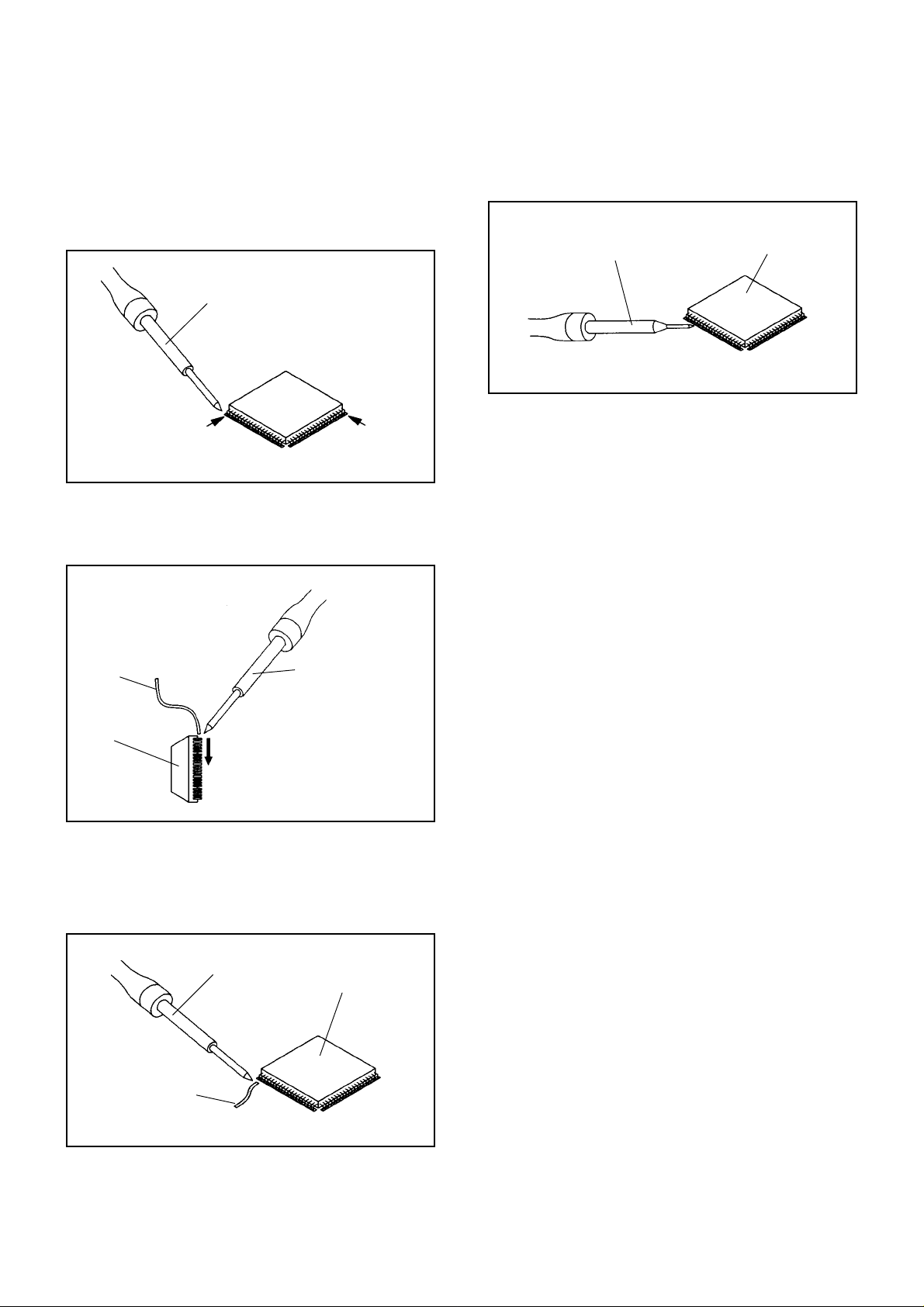
INSTALLATION
Take care of the polarity of new IC and then install the
1.
new IC fitting on the printed circuit pattern. Then solder
each lead on the diagonal positions of IC temporarily.
(Refer to Fig. 2-5.)
Soldering Iron
Solder temporarily
Solder temporarily
Fig. 2-5
Supply the solder from the upper position of IC leads
2.
sliding to the lower position of the IC leads.
(Refer to Fig. 2-6.)
When bridge-soldering between terminals and/or the
4.
soldering amount are not enough, resolder using a Thintip Soldering Iron. (Refer to Fig. 2-8.)
Thin-tip Soldering Iron
IC
Fig. 2-8
Finally, confirm the soldering status on four sides of the
5.
IC using a magnifying glass.
Confirm that no abnormality is found on the soldering
position and installation position of the parts around the
IC. If some abnormality is found, correct by resoldering.
NOTE
When the IC leads are bent during soldering and/or
repairing, do not repair the bending of leads. If the
bending of leads are repaired, the pattern may be
damaged. So, be always sure to replace the IC in this
case.
Soldering IronSolder
IC
Absorb the solder left on the lead using the Braided
3.
Supply soldering
from upper position
to lower position
Shield Wire. (Refer to Fig. 2-7.)
NOTE
Do not absorb the solder to excess.
Soldering Iron
IC
Braided Shield Wire
Fig. 2-6
Fig. 2-7
B-3
Page 11
SERVICE MODE LIST
This unit provided with the following SERVICE MODES so you can repair, examine and adjust easily.
The SERVICE MODE dose not funtion if the clock has been set.
if so, unplug AC cord to set the clock to the nonclock setting mode.
To enter the Service Mode, press both set key and remote control key for more than 1 second.
Set Key
Remocon Key
VOL. (-) MIN 1
Initialization of the factory.
NOTE: Do not use this for the normal servicing.
Operations
POWER ON total hours is displayed on the screen.
Refer to the "CONFIRMATION OF USING HOURS".
VOL. (-) MIN 6
Can be checked of the INITIAL DATA of MEMORY IC.
Refer to the "NOTE FOR THE REPLACING OF MEMORY IC".
VOL. (-) MIN
VOL. (-) MIN
VOL. (-) MIN
7
8
9
Releasing of PROTECTION PASSWORD.
Writing of EEPROM initial data.
NOTE: Do not use this for the normal servicing.
Display of the Adjustment MENU on the screen.
Refer to the "ELECTRICAL ADJUSTMENT" (On-Screen Display Adjustment).
CONFIRMATION OF USING HOURS
POWER ON total hours can be checked on the screen. Total hours are displayed in 16 system of notation.
NOTE: The confirmation of USING HOURS does not function if the clock has been set.
If so, unplug AC cord to set the clock to the nonclock setting mode.
1.
Set the VOLUME to minimum.
2.
Press both VOL. DOWN button on the set and Channel
button (6) on the remote control for more than 1 second.
3.
After the confirmation of using hours, turn off the power.
ADDRESS DATA
INIT 00 83
CRT ON
0010
FIG. 1
Initial setting content of MEMORY IC.
POWER ON total hours.
= (16 x 16 x 16 x thousands digit value)
+ (16 x 16 x hundreds digit value)
+ (16 x tens digit value)
+ (ones digit value)
NOTE FOR THE REPLACING OF MEMORY IC
If a service repair is undertaken where it has been required to change the MEMORY IC, the following steps should be taken to
ensure correct data settings while making reference to TABLE 1.
NOTE:
The confirmation of USING HOURS does not function if the clock has been set.
•
If so, unplug AC cord to set the clock to the nonclock setting mode.
•
No need the setting for after INI F3.
INI +0
E0
F0
00
+1
00 00
+3 +4 +5
0A
-
00
+6 +7
00 00
+8 +A
00
F4 94 60---
+9
D0 13 28 00
+2
Table 1
1.
Enter DATA SET mode by setting VOLUME to minimum.
2.
Press both VOL. DOWN button on the set and Channel button (6) on the remote control for more than 2 seconds.
ADDRESS and DATA should appear as FIG 1.
3.
ADDRESS is now selected and should "blink". Using the SET + or - keys on the remote, step through the ADDRESS until
required ADDRESS to be changed is reached.
4.
Press ENTER to select DATA. When DATA is selected, it will "blink".
5.
Again, step through the DATA using SET + or - until required DATA value has been selected.
6.
Pressing ENTER will take you back to ADDRESS for further selection if necessary.
7.
Repeat steps 3 to 6 until all data has been checked.
8.
When satisfied correct DATA has been entered, turn POWER off (return to STANDBY MODE) to finish DATA input.
The unit will now have the correct DATA for the new MEMORY IC.
+D +F
+E+B +C
00
C-1
Page 12

ELECTRICAL ADJUSTMENTS
1. BEFORE MAKING ELECTRICAL
ADJUSTMENTS
Read and perform these adjustments when repairing the
circuits or replacing electrical parts or PCB assemblies.
CAUTION
•
Use an isolation transformer when performing any
service on this chassis.
•
Before removing the anode cap, discharge electricity
because it contains high voltage.
•
When removing a PCB or related component, after
unfastening or changing a wire, be sure to put the wire
back in its original position.
Inferior silicon grease can damage IC's and transistors.
•
When replacing IC's and transistors, use only specified
silicon grease (YG6260M).
Remove all old silicon before applying new silicon.
Prepare the following measurement tools for electrical
adjustments.
1. Synchro Scope
2. Digital Voltmeter
3. Color Bar Generator
2. BASIC ADJUSTMENTS
On-Screen Display Adjustment
1.
Unplug AC cord to set the clock to the nonclock setting
mode. And then set the volume to minimum.
2.
Press both VOL. DOWN button on the set and the
Channel button (9) on the remote control for more than
1 second to appear the adjustment mode on the screen
as shown in Fig. 2-1.
NOTE
Use the Channel buttons (1-8) on the remote control to
select the options shown in Fig. 2-1.
Press the Channel button (0) on the remote control to
end the adjustments.
1. H/V
2. AKB
3. COLOR TEMP
4. PICTURE
5. OTHERS
6. TEST PATTERN
7.
8. (VOL TEST) 0. END
2-1: RF AGC DELAY
1.
Receive monoscope pattern.
2.
Connect the digital voltmeter to pin 5 of CP101.
3.
Activate the adjustment mode display of Fig. 2-1 and
press the channel button (5) on the remote control to
select "OTHERS". The Fig. 2-2 appears on the display.
4.
Press the channel button (2) on the remote control to
select "RF AGC RELAY".
5.
Press the VOL. UP/DOWN button on the remote control
until the digital voltmeter is 1.4 ± 0.05V.
Fig. 2-1
1. AGC AUTO
2. RF AGC DELAY
3. VIDEO LEVEL
4. FM LEVEL
5. OSD H
6. CUT OFF
7.
8. 0. RETURN
2-2: VCO
1.
Receive the color bar pattern.
2.
Connect the digital voltmeter to TP202.
3.
Adjust the L204 until the digital voltmeter is 3.5 ± 0.05V.
2-3: CUT OFF
Place the set with Aging Test for more than 15 minutes.
1.
Set condition is AV MODE without signal.
2.
Using the remote control, set the brightness and
3.
contrast to normal position.
Activate the adjustment mode display of Fig. 2-1 and
4.
press the channel button (5) on the remote control to
select "OTHERS". The Fig. 2-2 appears on the display.
Press the channel button (6) on the remote control to
5.
select "CUT OFF".
Adjust the Screen Volume until a dim raster is obtained.
6.
2-4: FOCUS
Using the remote control, set the brightness and
1.
contrast to normal position.
Receive the monoscope pattern.
2.
Turn the Focus Volume fully counterclockwise once.
3.
Adjust the Focus Volume until picture is distinct.
4.
2-5: WHITE BALANCE
NOTE:
1.
2.
3.
4.
5.
6
7.
8.
9.
Adjust after performing CUT OFF adjustments.
Place the set wiht Aging Test for more than 10 minutes.
Receive the white 100% signal from the Pattern
Generator.
Using the remote control, set the brightness and contrast
to normal position.
Activate the adjustment mode display of Fig. 2-1 and
press the channel button (2) on the remote control to
select "AKB". The Fig. 2-3 appears on the display.
Press the channel button (2) on the remote control to
select the "R.BIAS".
Using the VOL. UP/DOWN on the remote control, adjust
the R.BIAS.
Press the CH. UP/DOWN button on the remote control to
select the "G.BIAS", "B.BIAS", "R.DRIVE", or "B.DRIVE".
Using the VOL. UP/DOWN button on the remote control,
adjust the G.BIAS, B.BIAS, R.DRIVE or B.DRIVE.
Perform the above adjustments 7 and 8 until the white
color is looked like a white.
Fig. 2-2
D1-1
Page 13

ELECTRICAL ADJUSTMENTS
1. AKB AUTO
2. R. BIAS
3. G. BIAS
4. B. BIAS
5. R. DRIVE
6. G. DRIVE
7. B. DRIVE
8. 0. RETURN
2-6: BRIGHTNESS
Receive the monoscope pattern. (RF Input)
1.
Using the remote control, set the brightness and contrast
2.
to normal position.
Activate the adjustment mode display of Fig. 2-1 and
3.
press the channel button (4) on the remote control to
select "PICTURE". The Fig. 2-4 appears on the display.
Press the channel button (1) on the remote control to
4.
select "BRIGHT".
Press the VOL. UP/DOWN button on the remote control
5.
until the white 25% is starting to be visible.
Receive the monoscope pattern. (Audio Video Input)
6.
Press the AV button on the remote control to set to the
7.
AV mode. Then perform the above adjustments 2~5.
1. BRIGHT
2. CONTRAST
3. COLOR
4. TINT
5. SHARPNESS
6. OSD CONT
7.
8. 0. RETURN
Fig. 2-3
Fig. 2-4
0%
85%
100%
Fig. 2-5
2-8: CONTRAST
1.
Receive the monoscope pattern.
2.
Activate the adjustment mode display of Fig. 2-1 and
press the channel button (4) on the remote control to
select "PICTURE". The Fig. 2-4 appears on the display.
3.
Press the channel button (2) on the remote control to
select "CONTRAST".
4.
Press the VOL. UP/DOWN button on the remote control
until the bar step is set to the "24".
2-9: HORIZONTAL PHASE
1.
Receive the monoscope pattern.
2.
Using the remote control, set the brightness and
contrast to normal position.
3.
Activate the adjustment mode display of Fig. 2-1 and
press the channel button (1) on the remote control to
select "H/V". The Fig. 2-6 appears on the display.
4.
Press the channel button (1) on the remote control to
select "H. PHASE".
5.
Press the VOL. UP/DOWN button on the remote control
until the SHIFT quantity of the OVER SCAN on right
and left screen edges are equal.
2-7: COLOR
1.
Receive the color bar pattern. (RF Input)
2.
Connect the oscilloscope to TP802.
3.
Using the remote control, set the brightness, contrast,
color and tint to normal position.
4.
Activate the adjustment mode display of Fig. 2-1 and
press the channel button (4) on the remote control to
select "PICTURE". The Fig. 2-4 appears on the display.
5.
Press the channel button (3) on the remote control to
select "COLOR".
6.
Adjust the VOLTS RANGE VARIABLE knob of the
oscilloscope until the range between white 100% and 0%
is set to 4 scales on the screen of the oscilloscope.
7.
Press the VOL. UP/DOWN button on the remote control
until the red color level is adjusted to 3.2 scales (85%) ± 5%
for the white level. (Refer to Fig. 2-5)
8.
Receive the color bar pattern. (Audio Video Input)
9.
Press the AV button on the remote control to set to the
AV mode. Then perform the above adjustment 2~7.
1. H. PHASE
2. H. BLK
3. V. SIZE
4. V. POSI
5. V. LIN 50/60
6. V. SC 50/60
7. V. COMP
8. (H. FREQ) 0. RETURN
2-10: VERTICAL POSITION
1.
Receive the monoscope pattern.
2.
Using the remote control, set the brightness and
contrast to normal position.
3.
Activate the adjustment mode display of Fig. 2-1 and
press the channel button (1) on the remote control to
select "H/V". The Fig. 2-6 appears on the display.
4.
Press the channel button (4) on the remote control to
select "V. POSI".
5.
Press the VOL. UP/DOWN button on the remote control
until the horizontal line of the monoscope comes to
approximate center of the CRT.
Fig. 2-6
D1-2
Page 14

ELECTRICAL ADJUSTMENTS
2-11: VERTICAL SIZE
1.
Receive the monoscope pattern.
2.
Using the remote control, set the brightness and contrast
to normal position.
3.
Activate the adjustment mode display of Fig. 2-1 and
press the channel button (1) on the remote control to
select "H/V". The Fig. 2-6 appears on the display.
4.
Press the channel button (3) on the remote control to
select "V. SIZE".
5.
Press the VOL. UP/DOWN button on the remote
control until the SHIFT quantity of the OVER SCAN on
upside and downside becomes 8 ± 3%.
2-12: VERTICAL LINEALITY
Receive the monoscope pattern.
1.
Using the remote control, set the brightness and
2.
contrast to normal position.
Activate the adjustment mode display of Fig. 2-1 and
3.
press the channel button (1) on the remote control to
select "H/V". The Fig. 2-6 appears on the display.
Press the channel button (5) on the remote control to
4.
select "V. LIN 50/60".
Press the VOL. UP/DOWN button on the remote control
5.
until the SHIFT quantity of the OVER SCAN on upside
and downside becomes minimum.
Receive the monoscope pattern. (Audio Video Input)
6.
Press the AV button on the remote control to set to the
7.
AV mode. Then perform the above adjustments 2~5.
2-13: OSD HORIZONTAL
1.
Using the remote control, set the brightness and
contrast to normal position.
2.
Activate the adjustment mode display of Fig. 2-1 and
press the channel button (5) on the remote control to
select "OTHERS". The Fig. 2-2 appears on the display.
3.
Press the channel button (5) on the remote control to
select "OSD H".
4.
Press the VOL. UP/DOWN button on the remote control
until the difference of A and B becomes minimum.
(Refer to Fig. 2-7)
2-14: TINT
1.
Receive the color bar pattern.(Audio Video lnput)
2.
Connect the oscilloscope to TP801.
3.
Activate the adjustment mode display of Fig. 2-1 and
press the channel button (4) on the remote control to
select "PICTURE". The Fig. 2-4 appears on the display.
4.
Press the channel button (4) on the remote control to
select "TINT".
5.
Press the VOL. UP/DOWN button on the remote control
until the waveform becomes as shown in Fig. 2-8.
"TINT"
Fig. 2-8
2-15: CONSTANT VOLTAGE
1.
Using the remote control, set the brightness and
contrast to normal position.
2.
Connect the digital voltmeter to TP501.
3.
Set condition is AV MODE without signal.
4.
Adjust the VR501 until the DC voltage is 135 ± 1V.
A
OSD H
[ TV ]
B
Fig. 2-7
D1-3
Page 15

ELECTRICAL ADJUSTMENTS
3.
PURITY AND CONVERGENCE
ADJUSTMENTS
NOTE
Turn the unit on and let it warm up for at least 30
1.
minutes before performing the following adjustments.
Place the CRT surface facing east or west to reduce the
2.
terrestrial magnetism.
Turn ON the unit and demagnetize with a Degauss Coil.
3.
3-1: STATIC CONVERGENCE (ROUGH ADJUSTMENT)
1.
Tighten the screw for the magnet. Refer to the adjusted
CRT for the position. (Refer to Fig. 3-1)
If the deflection yoke and magnet are in one body,
untighten the screw for the body.
2.
Receive the green raster pattern from the color bar
generator.
3.
Slide the deflection yoke until it touches the funnel
side of the CRT.
4.
Adjust center of screen to green, with red and blue on the
sides, using the pair of purity magnets.
5.
Switch the color bar generator from the green raster
pattern to the crosshatch pattern.
6.
Combine red and blue of the 3 color crosshatch pattern
on the center of the screen by adjusting the pair of
4 pole magnets.
7.
Combine red/blue (magenta) and green by adjusting the
pair of 6 pole magnets.
8.
Adjust the crosshatch pattern to change to white
by repeating steps 6 and 7.
3-2: PURITY
NOTE
Adjust after performing adjustments in section 3-1.
Receive the green raster pattern from the color bar
1.
generator.
Adjust the pair of purity magnets to center the
2.
color on the screen.
Adjust the pair of purity magnets so the color at the
ends are equally wide.
Move the deflection yoke backward (to neck side)
3.
slowly, and stop it at the position when the whole
screen is green.
Confirm red and blue colors.
4.
Adjust the slant of the deflection yoke while watching the
5.
screen, then tighten the fixing screw.
DEFLECTION YOKE
DEFLECTION YOKE SCREW
MAGNET SCREW
3-3: STATIC CONVERGENCE
NOTE
Adjust after performing adjustments in section 3-2.
1.
Receive the crosshatch pattern from the color bar
generator.
2.
Combine red and blue of the 3 color crosshatch pattern
on the center of the screen by adjusting the pair of
4 pole magnets.
3.
Combine red/blue (magenta) and green by adjusting the
pair of 6 pole magnets.
3-4: DYNAMIC CONVERGENCE
NOTE
Adjust after performing adjustments in section 3-3.
1.2.Adjust the differences around the screen by moving
the deflection yoke upward/downward and right/left.
(Refer to Fig. 3-2-a)
Insert three wedges between the deflection yoke and
CRT funnel to fix the deflection yoke.
(Refer to Fig. 3-2-b)
R G B
R
G
B
UPWARD/DOWNWARD
SLANT
WEDGE
RIGHT/LEFT
SLANT
Fig. 3-2-a
WEDGE
WEDGE POSITION
Fig. 3-2-b
R
G
B
WEDGE
R G B
Fig. 3-1
PURITY MAGNETS
6 POLE MAGNETS
4 POLE MAGNETS
D2-1
Page 16

L204
MAJOR COMPONENTS LOCATION GUIDE
TP202
CP101
TU001
IC201
J753 J752
TP801
MAIN PCB
TP802
J801
VR501
TP501
FB401
FOCUS VOLUME
SCREEN VOLUME
CRT PCB
D3-1
Page 17

SP351
SPEAKER
SP352
SPEAKER
CH DOWN
CH UP/DOWN
VOL DOWN
VOL UP
Q502
TV POWER
SW
Q503
BUFFER
Q504
+B DRIVE
T501
12 16
5
9
OS101
Q505
RELAY SW
1
4
Q302
A_MUTE SW
1
2
3
5V REG. IC
IC502 KIA7805API
AT + 5.6V
RESET IC
IC103 PST600C
3
1
STAND BY
D106
F502
D501~D504
RECTIFIER
IC352 AN7523
4
SOUND AMP
2
MICON IC
IC101 OEC6056A
A_MUTE
2
9
KEY
31
REMORT
POWER
44
RESET
29
AV1
6
AV2
7
ATS
8
STAND BY LED
13
RY501
1
(MONO) IC
1
9
43
21
3
Q103
BUFFER
XIN
XOUT
OSD Y
18OSD R
19OSD G
20OSD B
35SCL
36SDA
27
28
21
23V-SYNC
22H-SYNC
X101
8MHz
2
1
Q201
Q101
V-BUFFER
Q102
H-BUFFER
L502
4
3
L501
13
24
TU001
SDA
BPLIF
11
IF AMP
MEMORY IC
IC102 S-24C08ADPA-01
7
SCL
6
SDA
5
54
BLOCK DIAGRAM
IF/CHROMA IC
5
Q807
AMP
+
IC201 LA76812
15
4
6
5
19
20
21
12
11
28
17
51
G-DRIVE
AGC
SCL
1
CF201
SAW FILTER
41
V-OUT IC
IC401 LA7840
725
PUMP UP
4
IF/RF AGC
VIF
AMP
OUT-OFF
DRIVE/
OSD
TRAP
BUS
FBP
SW
FM
DET
VIDEO
DET
SW
RGB
MATRIX
CONTRAST
BRIGHT
VIDEO
SW
AFC2
PHASE
SHIFTER
L204
Q851
BUFFER
DC
VOL
VIDEO
AMP
COLOR
CLAMP
SYNC
SEP
A2C
PLL
48
48 49
3
CLAMP
LIM
AMF
IDENT
VCO
TINT
DEMO
VER
RAMP
CLMP
HDR
OUT
49
1
64
DECORDER IC
IC850 ET106
22
20
19
23
16
14
2
54
52
IF
46
38
4.433619MHz
23
18
42
27
44
X601
Q301
BUFFER
Q402
H. DRIVE
Q401
H. OUTPUT
10
15
12
2
Q852
SYNC BUFFER
Q607
CLAMP SW.
Q804
Q802
R-DRIVE
B-DRIVE
IC402
KIA7805API
5V REG. IC
DATA SLICER IC
IC851 ET317
1211
13
17
19
9V REG. IC
IC403 KIA7809API
1
31
9
3
Heater
4
F
5
6
3
7
RGB
8
13875KHz
CRT
X850
E-1
POWER CONTROL IC
IC501 TDA16846
13
3
Q501
SWITCHING
+B ADJ
VR501
2
13
L503
DEGAUSS COIL
TH501
2
AUTO DEGAUSS
IN AC
34
1
SW501
Q701
F501
J702
BUFFER
EEH
3
H
AV SIGNAL
SWITCHER IC
IC751 LA7151
5
3
10
1
J752
1
21
4
2
EEH
3
4
H
VIDEO SW IC
IC701 NJM2245L
5
6
7
J753
3
Q611
BUFFER
Q754
VIDEO
OUT
21
H
E
4
H
E
FB401
1
FBT
4
9
10
F
S
HV
E-2
Page 18

PRINTED CIRCUIT BOARDS
MAIN/CRT (INSERTED PARTS)
SOLDER SIDE
F-1
PH002
TU001
S902Y
CC002
AGC
ADR
SCL
SDA
V.S
BPL
BTL
CP101_1
W007
W010
W008
R212
R213
W029
R145
NC
NC
NC
IF
W177
R206
S807Y
CF202
W109
C622_1
C308_1
W851
W036
W149
W001
W034
C101
L204
IC102
W188
R301
C212
D110
W006
W017
W016
W926
B301
W030
W009
R124
W027
W110
C301
C302
C204
L605
L301
D109
C003
L001
W018
R107
R105
W031
C001
L753
TP001
W111
R754
W108
W068
C110
W023
C002
W935
D001
CP852A
W013
W159
C760
C203_1
W032
W020
CF201
TP202
C213
W028
W923
W033
Q754
R776
C766
W167
D754_1
L202
C208
W174
W154
C644
W047
R775
IC751
C618
W024
R756
C767
W871
R630
W038
C755
W043
C609
C303
W928
W080
W048
J753
W045
W073
W046
IC201
W075
W936
C775_1
W920
W022
R612_1
C620
C626
C647
W061
S810X
W041
X101_1
W818
W044
S811X
W135
R656
L760
W039
D601
CP851A
W042
C614
D609
R629
C648_1
L101
W060
X601
W019
C632
R657
J752
R772
W879
D608
C109
C607
S811Y
C610_2
C628
C103
C751
D103
IC103
C111
21T
C616
W162
D614
D612
W137
C412
W025
D613
D615
W106
L758
C774
W003
C617_1
W132
C656
D623
W896
W011
OS101
W938
C608
W004
R414
S803Y
C403
D621
R128
R126
W005
W859
W858
W081
W839
W012
C606
D619
CP701
W105
S810Y
D767
W161
W134
W090
W087
R713
W838
D616
C641
C712
W932
D610
S808Y
S808X
CP802A
S902X
D622
R435
D104
D105
D106
R431
R411
R404
W099
W849
W095
TP803
C426_1
W185
W101
C423
W089
R336
R804
W880
IC402
R416
R419
W186
C125
W922
S807X
W191
S903X
CP351_1
R808
TP801
Q807
C804
R811
W091
S803X
C429
W122
R813
HS403
C418_1
C417
W893
R306
C319
W198
C810
R410
R418
L701
R806
TP802
Q802
C820
S801Y
R417
C415
W201
R822
R412
C414
W873
W810
S801X
W807
R821
Q804
R823
C313_1
R817
R819
CH UP
SW107
R430
R407_2
R425
R420
C410
D403
C425
W902
C350
IC701
C708
CP804
21T
C430
R402
C439
IC352
D702
C707
CD804
J801
C317
W166
R816
IC401
R446
Q402
W085
C701
D701
C703
C718
W903
C807
CP802B
C427
R432
C413
L410
C320
R523
Q504
R519
D514
D512
D511
C806_1
R815
C802_1
21T
20 CH DOWN
14 CH UP/
HS402
C440
HS352
S903Y
R521
R423
C408
W074
C446
Q503
SW106
CP401
C401_1
W088
T401
W084
W096
R517
D516
L401
R401
C437
R002
R001
W802
D515
C519
C516_1
C518
R511
C534
R516
R520
CH DOWN
W053
FH504
VOL UP
SW104
C443
C405_1
C524
W054
W157
W163
CP801
C535
W057
R448
W194
F502
R505
CP803B
C521
R406
W058
C529
R504
W117
W119
W092
CP803A
W116
W115
IC403
TP501
R524
ICP501
D510
FH503
D506
C517
R522
R533
Q502
IC502_1
VOL DOWN
D401
W811
B503
SW102
21T21T
R434
C433
Q505
W856
W056
W189
D513
W094
C448
B504
RY501
C444_1
R427
W055
TH501
C520
CC001
D407
C502
CP502
Q401
C416
R429
HS501
C532
W862
T501
SW501
R421
R422
D405
W113
HS401
C501
W052
C514_1
C435
C409
D505
B401
R405
R428
C420
D410
W059
B502
C515
L406
Q501
W050
B501
L501_1
13V
NC
180V
25V
C512
R514
FH501
C531
C508
C506
F501
GND
VR501
C513
R526
C507
D501
ABL
R512
D508
W051
D404
R408
HEATERAFC
W917
R532
W145
CP501
C533
C503
R529
D503
C526
W863
FB401
D507
D504
D509
C505
R501
L502
R530
R525
C525
C527
C510
PH001
R513
B+
R527
D502
C504
COL
IC501
C511
R503
FH502
F-2
Page 19

PRINTED CIRCUIT BOARDS
MAIN (CHIP MOUNTED PARTS)
SOLDER SIDE
R103
R138
C522
C704
C719
C706
C702
W130
R703
R139
W819
W156
R350
R305
W877
R330
Q302
R331
W124
R704
W098
R710
Q701
W121
R102
R709
W199
W869
R711
C710
R649
R638
R636
C404
R409
W200
R133
W129
R637
C108
W927
C652
R650
C639_1
C407
C642
R634
R123
R129
R134
C645
R130
W813
Q607
R623
R627
R127
Q101
C104
Q102
W865
C120
C114
R653
C105
W894
C627
R652
W870
C119
C121
R643
R651
R613
C118
R120
C624
C615
W868
R624
C113
23
R654
R327
R631
C621
R136
12
IC101
R137
R622
R210
C116
34
R114
R617
C214
C215
R111
R225
R208
R226
R142
R112
R615
C207
C206
R101
W803
R302
C209
R204
R708
1
R312
C305
R216
C307
R211
Q201
R109
R143
C304
C306
R207
R201
C202
R108
C107
C205
Q301
R202
R307
C123
C201
R205
R110
R122
R616
R308
R121
Q611
R641
C655
C220
R209
R215
C112
W812
Q103
C124
R113
W120
R218
W855
B101
F-3
R131
R132
W190
R403
W128
W808
W850
W933
W918W921
W809
W885
R778
C762
R601
R759
C765
W197
R758
W900
R003R004
C758
C008
C007
F-4
Page 20

T' TEXT (INSERTED PARTS)
SOLDER SIDE
PRINTED CIRCUIT BOARDS
T' TEXT (CHIP MOUNTED PARTS)
SOLDER SIDE
TE9A15A
C865
C852
X850
CP852B
C877
IC851
W851
W854
L852
R885
W858
W007
W860
L851
CP851B
W865
R869
W005
W003
C868
TE9A15A
W004
W853
W002
W863
IC850
C869
C855
Q851
B850
C870
FRONT AV JACK
SOLDER SIDE
Q852
W868
R871
W861
W001
R880
R867
R875
C861
R854
C867
R857
R881
W867
R853
R855
W008
R851
C860
W859
C858
R852
C886
C887
C883
W857
R870
W870
C879
C880
C876
C864
C884
W864
R864
R879
C881
R865
F-5
CD701
J702
F-6
Page 21

ABC DEF GH
8
TEST POINT
CP101_1
7
8283_0612_00_000
1
2
3
4
5
6
FROM/TO IF/CHROMA/SOUND AMP
6
T_TEXT_RESET
5
4
3
MICON/TUNER SCHEMATIC DIAGRAM
OS101
GP1U281Q
GND
B+
Vout
123
R107
R105
100
100
0.0
0.0
0.0
0.0
DTC114TKA
1K
S-24C08ADPA-01
1234
E0
E1
E2
VSS
BUFFER
Q103
MEMORY IC
IC102
D109MTZJ5.6B
5.0
0.0
R109
10K
R1421.2K
W936
(W076)
5.2
VCC
0.0
MODE
C123
SCL
4.8
5678
SDA
4.8
4.8
R108
10K
R110
22K
STAND BY
D106
SLR-342VCT32
OSD-R
OSD-G
OSD-B
OSD-Y
AFC
220P
C112
CH
C124
D110
MTZJ5.6B
MICON IC
IC101
OEC6056A
0.01 B
C101
1006.3V KS
R124
100
CH
R113
220P
100
NC
NC
4.6 4.8 5.0 5.0 0.0 4.9 0.0 5.0 4.9 4.8 0.0
4.9
11011
T_RESET
4.4
A_MUTE
0.0
3
BLUE BACK H
NC
0.0
DEGAUSS
NC
0.0
56789
YS MUTE
NC
4.8
AV1
4.8
AV2
4.8
ATS
4.9
KEY
4.8
AFT
5.2
FORTHED VCR V-SYNC
12 13 14 15 16 17 18 19220 21 22
NC
R114
270
PAL/SEC
12 9V POWER
13 STAND BY LED
14 ON TIME LED
22 H-SYNC
NC
NC NC
VSS
VSS
VDD
4.4 4.4 4.4 4.4 4.90.00.00.00.33.80.8
NC
R143
R121 3.3K
NCNC
12C OFF
34 SOUND B
35 SCL
43 AKB WHITE
44 POWER21 OSD Y
OSD G
OSD R
W870
W868
W869
C113 220PCHC116 220PCHC118 220P
SDA
OSD B
C119 100P CH
CH
4.7K
R112
R122 3.3KR120 1KR123 3.3K
12
34353637383944041424344
SOUND A
SD
REMORT
P_FAIL
RESET
XOUT
XIN
TEST
OSC OUT
OSC IN
C120
GND
I2C_SCL
I2C_SDA
I2C_OFF
AGC
AFT
TUNER_AGC
TUNER_IF
AFT POWER_FAIL
SDA
SCL 130V
OSD-R POWER
OSD-G
OSD-B
OSD-Y
AFC
A_MUTE
R145
TO JACK
AV1
AV2
R111
4.7K
5.04.80.0
1050V KS
C103
47
R126
22K
22K
R136
5.0
5.0
5.0
30 31 32 33
4.2
X101_1
5.0
8MHz
3.8
4.4
W818
0.0
5.0
4.9
23 24 25 26 27 28 29
5.2
5
4
180P CH
L101
3
33uH
22K
R137
C108 0.1 B
C114 22PCH
C121 27PCH
C104 12PCH
C10512PCH
C107
C110
0.01 B
S902Y
B101
BLM21A601SPT
33006.3V YK
(MAIN PCB)
TU001 TUWOF4EG-771F2
IF
11
10
14 15
NC NC NC NC
0.1
0.0
TP001
D001 HZ30-3L
C001
C008
0.01B
D104
1S2472
RESET IC
IC103 PST600C
10K
R133
VCC
GND
123
4.9 0.0 5.0
D103
1SS133
150V KS
C111
R001
31.2
0.022 M
BTL
9
R002
V.OUT
0.0
68K 1/2W
8
R134
L001
68K 1/2W
PH001
003P-2100
NC
BPL
V.S
SDA
SCL
ADRES
AGC
2
3
4
5
6
7
NC
4.8
0.0
3.2
3.2
270
R003
10uH
0607
10006.3V YK
R004
C002
YK
4706.3V
C125
D105
11E1N
10K
1
3.9
270
12 13
0.0
2.6
C003
4.750V
C007
0.01B
PH002
003P-2100
KS
FROM DEFLECTION/CRT
FBT_5V
VD
FROM/TO POWER
AT+5.6V
GND
FROM IF/CHROMA/SOUND AMP
FBT_5V
AT+5V
GND
8
7
6
5
4
3
R138
2.2K
R101
ACCESSORY
2
ANT001
T4-216BP-BK
1
BT001
R03(AB)E_20_T
BT002
R03(AB)E_20_T
TM101
SBER00192A
NOTE:THIS SCHEMATIC DIAGRAM IS THE LATEST AT THE TIME
OF PRINTING AND SUBJECT TO CHANGE WITHOUT NOTICE
R102
390
20 VOL UP
SW102
R103
820
SKHVBED010
SW104
20 VOL DOWN
SKHVBED010
1.2K
SW106
20 CH UP/14 DOWN
NOTE:
WITH THE DIGITAL TESTER WHEN THE COLOR BROADCAST
R139
2.2K
SW107
SKHVBED010
20 CH DOWN
THE DC VOLTAGE AT EACH PART WAS MEASURED
WAS RECEIVED IN GOOD CONDITION AND PICTURE IS NORMAL.
SKHVBED010
R131
R132
10K
820
R130
4.9
3.9
H-BUFFER
Q102
2SC2412K
0.0
15K
1K
R127
V-BUFFER
Q101
2SC2412K
33K
R128
5.2
0.1
0.0
C109
2.2K
R129
0.015 M
PCB010
TM9430
CAUTION: DIGITAL TRANSISTOR
2
1
ABC DEF GH
G-2G-1
Page 22

ABC D E F GH
8
FROM/TO JACK
TUNER_AUDIO_R
AV_AUDIO
7
6
5
AV_VIDEO_2
TU_VIDEO_OUT
DET_OUT
FROM/TO VIDEO/R.G.B SWITCH
VIDEO_OUT[1]
AV_VIDEO_1
A-R
A-G
A-B
A-Y
GND
FROM/TO T’TEXT
CP852A
IMSA-9130B-05
1
AV_VIDEO_2
2
SDA
3
SCL
4
T_TEXT_RESET
5
AT+5V
FROM/TO MICON/TUNER
4
FBT_5V
AT+5V
T_TEXT_RESET
TUNER_IF
A_MUTE
3
TUNER_AGC
OSD-Y GND
OSD-R
OSD-G
OSD-B
2
TO VIDEO/R.G.B SWITCH
1
IF/CHROMA/SOUND AMP SCHEMATIC DIAGRAM
8
(MAIN PCB)
TO SOUND
FBT_5V
GND
FROM JACK
FBT_9V
FBT_5V
FROM/TO DEFLECTION/CRT
AFC
CLAMP
B.OUT
G.OUT
R.OUT
H_OUT
V_OUT
ACL
FBT_9V
FROM POWER
GND
AT+12V
SOUND+B
SOUND_GND
FROM/TO JACK
TO SOUND
SOUND_SP[-]
SOUND_SP[+]
7
6
5
4
3
2
1
G-4G-3
AFC
SDA
SCL
AFT
TEXT-B
TEXT-G
TEXT-R
GND
TEXT-Y
S811X
W923
R215
W900
R226
100
W926
0.022 B
75
CF202
A-Y
D612
FROM T’TEXT
CP851A
IMSA-9130B-06
BUFFER
Q611
2SA1037AK
S811Y
6.8K
R201
C201
1.0
2.2K
R202
MKT40.4MA110P
R.OUT
G.OUT
1SS133
D613
D614
1SS133
SYNC
TEXT-B
TEXT-G
TEXT-R
GND
TEXT-Y
4.2
0.0
R615
R616
C202
L202
R205
1SS133
1
2
3
4
5
6
470
470
2.8
0.0
0.022 B
2.2uH
IF AMP
2SC2814
47
B.OUT
D615
Q201
2.1
1SS133
R617
R204
1K
AV_AUDIO
1K
R302
C306
W803
C305
0.1 B
C304
47P CH
6
R312
2.8
BPF
SPLL
BPF
LIM
AMP
FM
DET
SW
DC
VOL
1 101112131415161718192 20 21 22 23 24 25 26 27
R301
C301
1K
R308
100
100
0.01 M
C302
C203_1
0.001 B
IF AGC
3
C204
0.015 M
0.001 B
C308_1 150V NP
C307
47P CH
330
RF AGC
4
R206
C205
0.01 B
0.022 M
12345
SAF38.9MAZ220Z
10K
R207
R225 100K
CF201
5051525354
C206
R218 270
VIDEO
5
120K
C214
AMP
TRAP
VIDEO
DET
VIF
R208
C212 0.4750V KS
0.001 B
0.01 B
10K
OUTOUTGININ
C213
VCO
6
1
NC
A2C
PLL
6789
0.4750V KS
L204
3600042
2
34
4.8
C207
0.01 B
4706.3V YK
C208
C215
S807Y
0.01 B
W871
NOTE:THIS SCHEMATIC DIAGRAM IS THE LATEST AT THE TIME
OF PRINTING AND SUBJECT TO CHANGE WITHOUT NOTICE
150V KS
C618
TP202
JWF-50K-1
R622
IF
IDENT
AFT
2.4 2.2 4.9 4.9 3.8 1.1 1.2 1.2 0.0 8.2 3.2 3.0 3.2 0.4 2.8 2.8 5.4 3.8 1.1
2.2K
R327
150V KS
C303
R210
100K
C209
R211
120K
0.01 B
C220
0.01 F
AFT
B301
W812
L301
15uH
3.0 2.3 2.3 2.6 4.1 4.1 3.6 2.4 1.8 4.8 3.2 2.0 0.0 2.6 3.4 2.7 3.7 0.4 2.4 0.0 0.0 8.0 4.8 0.8 1.8 2.2
IF/CHROMA IC
IC201 LA76812
BL02RN1-R62
R209
2.0 3.2 2.6 3.2 2.3 3.0 0.0
10K
W849
4.9
2.4
Q301
2SC2412K
1.8
BUFFER
W855
R307
100
470
7
AV_VIDEO_1
C621 0.01 B
W928
680K
C620 4706.3V YK
89
CLMP CLMP
VIDEO
SW
BAF SW
TRAP
DELAY
SYNC
LINE
SEP
PEAKING
BLACK
CORING
STRETCH
BUS ABL CLAMP
100
100
R213
R212
R654
R216
SDA
SCL
R656
1K
R657
1K
R627
0.150V NP
C622_1
C624 0.01 B
27uH
L605
C655
R641 330
R629 1K
47P CH
40414243444546474849
APC1
ACC
OSD
CONTRAST
W921
W922
10K
2.2K
A-R
A-G
A_MUTE
SOUND AMP (MONO) IC
IC352 AN7523
+
Vcc
1234567
W873
W813
X601
4.433619MHz
R631 24K
R630 24K
1050V KS
C647
R643
2.2M
C626
0.4750V KS
C627
16P CH
NCNC
3536373839
CW
KILLER
VCO
APC2
TINT
PAL
DEMO
W918
A-B
4.07.9 0.0 4.0 6.0 1.4 0.00.0
VCO
SW
CLAMP
CONTRAST
BRIGHT
4.7K
R305
C615
C614 47010V YK
R623
D621
A-Y
7.2
0.0
1K
0.0
R624
CLAMP
DC ADS.
RGB
MATRIX
OSD
SW
DRIVE/OUT-OFF B.AKB
100
R652
R651
0.01 B
39
D608 MTZJ8.2AD622
D623
MTZJ5.6B
MTZJ5.6B
R.OUT
G.OUT
W802
C350
0.0039 M
A_MUTE SW
Q302
2SC2412K
THE DC VOLTAGE AT EACH PART WAS MEASURED
NOTE:
WITH THE DIGITAL TESTER WHEN THE COLOR BROADCAST
WAS RECEIVED IN GOOD CONDITION AND PICTURE IS NORMAL.
SW
100
R653
MTZJ5.6B
B.OUT
R306
C644
W865
100
C639_1
D609
89
NC
470
HS352
S801XS807X
47010V YK
C632
1H DELAY
100P CH
C628
+
COLOR
CLAMP
VER
SEP
VER
C/D
RAMP
C616
1SS133
1713 12 11
V_OUT
150V KS
R336
R331
R330
4706.3V YK
C617_1 0.33 MMTV
0.22 TF
C609
LPF
ALC
22K
1.5K
8.2K
C403 4706.3V YK
W927
3031323334
HDRVER
VCC
R404
0.150V KS
56K +-1%
14
W896
C645
220P
CH
C404 0.01 B
180 1/2W
R612_1
R634
HDR
VCO
1/256
HDR
C/D
AFC1
R409
C412
W902
C652
4.7K +-1%
FBP
AFC2
PHASE
SHIFTER
HDR
OUT
4.7K
3.350V
R613
R350
W810
150P CH
2829
C407
YK
10K+-1%
H_OUT
6.8K
R435
R411
0.015 B
C642
C610_2
16
330
C656
100 1/4W
0.01 B
4.750V NP
C319
B
220P
D610
11E1N
D401
MTZJ5.6B
R434
10K
R649
4716V YK
C317
W859
10
AFC
R638
2.2K
R636
D619
1SS133
1.2K
CLAMP SW.
D616
1SS133
Q607
1.1
2SA1037AK
0.5
390
10016V YK
C641
C313_1
1035V KANP
10016V KA
R637
0.1
1K
15
R650
S803Y
S808Y
C320
100016V YK
W893
PCB010
TM9430
ABC D E F GH
Page 23

ABC D E F GH
SOUND SCHEMATIC DIAGRAM
47K
5.0
0.0
1K
R708
47K
(MAIN PCB)
BUFFER
Q701
2SC2412K
FROM IF/CHROMA/SOUND AMP
FBT_5V
GND
TO JACK
GND
EXT_VIDEO_IN
EXT_AUDIO_IN[L]
8
7
6
5
8
7
TO
FRONT AV JACK
6
CP701
8283_0712_00_000
1
NC
2
3
4
5
NC
6
7
75
R704
S808X
C710
R710
C712
R711
100
0.022 B
2.3
1050V KS
R709
5
FROM IF/CHROMA/SOUND AMP
W819
4
W877
1
2
CP351_1
TID-X02P-B2
CH01806A
CD351_1
CH22060A
1
2
SPEAKER
4 OHM 2.5W
SP351_1
3
MS-2D6SB02-1
4 OHM 2.5W
SP352_1
MS-2D6SB02-1
SPEAKER
CD352_1
2
SOUND_SP[-]
SOUND_SP[+]
PCB010
TM9430
4
3
2
THE DC VOLTAGE AT EACH PART WAS MEASURED
1
NOTE:THIS SCHEMATIC DIAGRAM IS THE LATEST AT THE TIME
OF PRINTING AND SUBJECT TO CHANGE WITHOUT NOTICE
NOTE:
WITH THE DIGITAL TESTER WHEN THE COLOR BROADCAST
WAS RECEIVED IN GOOD CONDITION AND PICTURE IS NORMAL.
1
ABC D E F GH
G-6G-5
Page 24

ABC D E F GH
POWER SCHEMATIC DIAGRAM
8
2A 125V
CAUTION:
FOR CONTINUED PROTECTION AGAINST FIRE HAZARD,
REPLACE ONLY WITH THE SAME TYPE FUSE
,1A 250V(F502)
ATTENTION: POUR UNE PROTECTION CONTINUE LES RISQUES D’INCEIE
7
N’UTILISER QUE DES FUSIBLE DE MEME TYPE
,1A 250V(F502)
ICP501 ARE MANUFACTURED BY
CAUTION:
LITTELFUSE INC.,TYPE 251.
1A 250V
AND 2A 125V (ICP501)
ET 2A 125V (ICP501)
4A 250V
4A 250V(F501)
6
C525
100P250V KX
5
C526
0.22250V MMCA
4
3
4
SW501
2
SDDFC30400
MAIN SWITCH
2
BLUE
0.22250V ECQUL
3
NC
NC
1
F501
T4A_L_250V
BROWN
12
C527
100P250V KX
SS24H-07200
C501
5 6
FH501
EYF-52BC
FH502
EYF-52BC
CP501
THL-P03P-B1
RY501
ALKS321
LINE FILTER
L502
FK0B160MH14
34
12
LINE FILTER
L501_1
34
3
12
4A 250V
D506
1S2472
RELAY SW
Q505
2SC2001_L
12
4
R501
AUTO DEGAUSS
TH501
PTH451C262BF140M
123
1.5M 1/2W
1
0.1
0.0
PH
2
0.7
R505
C502
CP502
TV-50P-02-A1
400V
10K 1/4W
0.0022250V KX
R530
12K
R503
5.6 7W
D502
RM11C
D501
RM11C
C505
100
HS501
C503
10025V YK
C533
330P B
W863
R532
W917
R504
10K 1/4W
C506
C507
USP
NC NC
R529
1/2W
1.5M
D503
RM11C
0.00222KV B
C508
0.0022500V B
0.00222KV B
D504
RM11C
R512
47 1/4W
POWER CONTROL IC
IC501 TDA16846
16V
OVERVOLTAGE
12.6
COMPARATOR
STARTUP
DIODE
5.2
DRIVER
G3
OUTPUT
0.0
R6
1.5V
3.6
1/2W
1V
10 11 12 13 14
0.0
1V
1M
5.8
VCC
89
NC
5.3 5.8
+
-
D1
OD
PVC
+
VOLTAGE
FLIPFLOP
-
+
+
-
COMPARATOR
OV
G2
1.5V
SIGNAL
ZERO CROSSING
FOLD BACK
R5
PVA
+
PRIMARY
S
R
ERROR
FC1
SUPPLY
VOLTAGE
CORRECTION
CHECK
68K 3W
SWITCHING
Q501
2SK2651-01MR
OFTC
OFF
TIME
COMPARATOR
G1
ON
S
TIME
QONTF
R
COMPARATOR
ONTC
DE2
D2
ED1
EA
POINT
D5
1)
BCV
QERR
BUFFER
CONTROL
FOR
VOLTAGE
G4
-
FC2
+
CONTROL
R4
D4
VOLTAGE
-
KSY
R7
+
R3
R8
15k5V75k
-
+
R513
2V
3.5V
R2
+
-
ERROR
+
+
-
1.2V
30k
+
-
AMPLIFIER
5V
(MAIN PCB)
8
7
TO DEFLECTION/CRT
130V
GND
R519
BUFFER
10K
Q503
2SA1371
+B DRIVE
Q504 2SC4160
136.4
136.6
136.3136.4
136.2
TP501
R523
10K
135.7
DE
6
R520
82K 1/4W
0
0.6
C529
R516
15 3W
15DF6-FC
FH504
EYF-52BC
470P500V B
D515
15DF6-FC
R524
2.2 5W
D510
C516_1
820P2KV YR
S903Y
D511
10ELS6
HZ36-1L
0.022630V PP
C513
B502
BL02RN2-R62
330P2KV BN
C515
D509
C514_1
330P2KV YR
C531
T501
8140051W
12.4
9
6.87
10
158.34
11
NC
136.28
12
75.44
NC
13
0
14
0
15
18.8
16
310.3
353.9
15.15
782.2
300
1
3
NC
4
5
6
NC
0
7
470P2KV BN
2A 125V
B504
BL01RN1-A63
B503
BL01RN1-A63
FH503
EYF-52BC
ICP501
251002
F502
T1A_L_250V
D507
HZ36-1L
R514
68K 3W
D505
1R5NU41
B501
BL01RN1-A63
280.0
D
G
8.0
0.0
S
1A 250V
1
2.2
234567
1.9
5V
1.7
D3
3.7
NC
R1
4.3
20k
0.0
+B ADJ
VR501
C512
4.7K
R527
0.015 M
5.6K
C511
R525
680P B
47K
R526
10K
C510
D508
C504
100P500V B
0.0018 M
10ELS6
C532
470P250V KX
CC001
CC002
C534
330P B
D512
10ELS6
TV POWER SW
Q502
2SC2909
100
C519
200V YK
47025V YK
C517
MTZJ7.5B
150V KS
C518
R511
C520
D514
0
ST
120K 1/2W
W856
10025V YK
R522
10K
C535
2210V KS
5V REG IC
IC502_1 KIA7805API
V.IN
GND
123
5.60.69.6
D513
C521
1SS133
R517
6.8K
C522
0.01 B
V.OUT
150V KS
R521
10K
D516
C524
R533
10K
MTZJ5.1B
47160V BXA
FROM/TO MICON/TUNER
GND
130V
POWER
AT+5.6V
POWER_FAIL
TO IF/CHROMA/SOUND AMP
GND
SOUND+B
SOUND_GND
AT+12V
PCB010
TM9430
5
4
3
2
21
AC240V_50Hz
BROWN
CD501
1206665817
BLUE
1
21
DEGAUSS COIL
L503
8H200015
CRITICAL FOR SAFETY,USE ONES
DESCRIBED IN PARTS LIST ONLY
THE DC VOLTAGE AT EACH PART WAS MEASURED
ARESINCE THESE PARTS MARKED BYCAUTION:
DANGEREUSES AN POINT DE VUE SECURITE
N’UTILISER QUE CELLS DECRITES
DANS LA NOMENCLATURE DES PIECES
ETANTLES PIECES REPAREES PAR UNATTENTION:
NOTE:
WITH THE DIGITAL TESTER WHEN THE COLOR BROADCAST
WAS RECEIVED IN GOOD CONDITION AND PICTURE IS NORMAL.
NOTE:THIS SCHEMATIC DIAGRAM IS THE LATEST AT THE TIME
OF PRINTING AND SUBJECT TO CHANGE WITHOUT NOTICE
1
ABC D E F GH
G-8G-7
Page 25

ABC DEF GH
DEFLECTION/CRT SCHEMATIC DIAGRAM
(MAIN PCB)
8
FROM/TO IF/CHROMA/SOUND AMP
GND
CLAMP
G.OUT
B.OUT
R.OUT
V_OUT
AFC
ACL
7
H_OUT
FBT_9V
TO MICON/TUNER
VD
FBT_5V
6
5
4
S803X
3
FROM POWER
130V
2
GND
H.DRIVE
Q402
2SC2688
R448
8.2K 5W
W811
C439
22P500V
27.0
0.3
19
IN GND OUT
11.7 0.0 9.1
R416
33 1W
SL
0.0
1160V YK
C446
C416
200V PP
0.012
IC402 KIA7805API
IN GND OUT
123
11.7 0.0 5.0
9V REG. IC
IC403 KIA7809API
123
C408
R430
1W
120
T401
B
470P500V
1/2W
4.7K
L406
18uH
12
305Y002
34
2
1
HS401
NC
R405
12 1/2W
R428
1/2W
S801Y
20
C440
R446
5V REG. IC
S902X S903X
V-OUT IC
IC401 LA7840
R417
R425
C405_1
VCC
47035V YK
C410
R418_1
12K+-1%
12K +-1%
+-1%
2.7 1/4W
ECWF
0.39250V
C437
22016V MHE
D410
PUMP
UP
C414
R419
C417
10ELS6
1K
2.250V KS
C420
10035V YK
R420
27K
129.0
129.0
129.0
C448
23
D403
11E1N
R410
C430_1
330 1/2W
2200
C418_1
25V MHE
1050V MHE
ABL
HEATER
+14V
C435
R408
1.5
GND
R432
HV
F
S
11
7
2.3
10
0.0
NC
5
0.2
TF
0.047100V
2W
C427
R407_2
2.7 1/4W
R401
1K 1W
C401_1
0.0012KV YR
L401
2R000008_1429MS
FB401
3220046F
COL
1
+180V
6
B
0.0011KV
B+
2
AFC
9
0.4
GND GND
8
0.0
+25V
34
0.6
W862
D407
10ELS6
R406
330K 1/2W
10200V MHE
D404
10ELS6
0.068100V
TF
1.2K 1/2W
THERMAL
PROTECTION
-
AMP
0.0022 B
C413
L410
R423
0.015 M
C443
500V
1250V YK
0909
4.7mH
68 1/2W
DKR
0.00471.6KV
C444_1
R422
3.3K 1/2W
C409
150P500V B
+
C415
100P
SL
820P2KV YR
GND
1234567
0.0 15.3 25.1 3.7 3.7 24.0 5.3
R414
1/4W
3.9K
15K
R402
C429
R431
R403
1.5K 1/4W
C426_1
22
129.0
0.0
MTZJ9.1B
0.0
D405
18K
220010V YK
B401
C423
BL01RN1-A63
4.750V KS
C425
HS402
100016V YK
6
H.OUTPUT
Q401
2SD2499
21
R427
100 1/4W
HS403
GND GND
CLAMP CLAMP
G.OUT G.OUT
B.OUT B.OUT
R.OUT R.OUT
51048-0510
R412
330 1/2W
R429
1W
3.9
47035V MHE
C433
R421
220K 1/2W
1
2
3
4
5
CP802A
24
51052-0400
DY801
5
4
3
NC
2
1
CP401
B05B-DVS
180V 180V
4
GND GND
3
GND GND
2
HEATER HEATER
1
CP803A
PCB010
TM9430
CD802
2E054201
5
4
3
2
1
CD801
CP83035A
V801
A51LMU50X50S50
9
10
R
8
G
6
B
11
FOCUS
SCREEN
2E043201
CORE FERRITE
ESD-R-30SD
TS-80P-03-V1
175
CD803
L802
CP801
1
2
3
CP804
005P-2100
180V
GND
GND
HEATER
1
2
3
4
5
CP802B
51048-0510
1
2
3
1
4
3
2
1
CP803B
51052-0400
PCB110
TC9290
W903
C806_1
J801
HPS3200-010501
R804
15K 2W
R806
15K 2W
R808
15K 2W
B-DRIVE
2SC4217
W807
Q802
0.00222KV
GREEN
TP803
TP802
BULE
TP801
3.8
RED
C802_1
100P B
B
GREEN
4.6
126.3
2.5
C807
139.0
BLUE
470P B
R821
R815
RED
2.7K 1/4W
R819
R817
2.7K 1/4W
2.7K 1/4W
G-DRIVE
Q807
139.0
2SC4217
W880
270
4.7K
C810
R816
3.1
2.4
4.7K
270
R823
470P B
R822
C804
C820
120.4
0
0
6
5
7
294.5
8
130.6
9
26
25
27
139.0
3.1
R811
470P B
0.001 B
4
3
1
F
0
R-DRIVE
Q804
2SC4217
3.2
270
R813
4.7K
8
7
6
5
4
3
2
1
NOTE:THIS SCHEMATIC DIAGRAM IS THE LATEST AT THE TIME
OF PRINTING AND SUBJECT TO CHANGE WITHOUT NOTICE
THE DC VOLTAGE AT EACH PART WAS MEASURED
NOTE:
WITH THE DIGITAL TESTER WHEN THE COLOR BROADCAST
WAS RECEIVED IN GOOD CONDITION AND PICTURE IS NORMAL.
CRITICAL FOR SAFETY,USE ONES
DESCRIBED IN PARTS LIST ONLY
ARESINCE THESE PARTS MARKED BYCAUTION:
DANGEREUSES AN POINT DE VUE SECURITE
N’UTILISER QUE CELLS DECRITES
DANS LA NOMENCLATURE DES PIECES
ETANTLES PIECES REPAREES PAR UNATTENTION:
1
ABC DEF GH
G-10G-9
Page 26

ABC D E F GH
JACK SCHEMATIC DIAGRAM
8
FROM MICON/TUNER
7
6
FROM/TO VIDEO/R.G.B SWITCH
5
4
(MAIN PCB)
IC751 LA7151AV SIGNAL SWITCHER IC
AV1
AV2
R754
220
1006.3V
YK
C760
330
R775
R776
330
GND
W935
AA
110
2.4 0 2.4 0 2.4 2.4 0
(W112)
CH1(L) CH2(R)
LL
NC
NC
C766
47010V YK
NP
1016V
29
C755
W920
C758
150P CH
S810X
C775_1
VIDEO OUT
Q754
2SC1815Y
2.8
2.14.8
R758
1050V YK
100
2.50
C767
47010V YK
HH
BB
11 1223456 789
2.5 0
5.0
R756
NC
NCNC
L753
10uH
0607
68
75
R759
L701
10uH
R713
220
3316V KS
C701
C718
VIDEO IN
VIDEO OUT
28
V.IN1
12345678
4.0
0.0
0.022 B
C719
C703
W839
100P CH
KS
1016V
C704
C702
10016V YK
IC701 NJM2245LVIDEO SW IC
BUFFER
15K
BIAS
15K
SW1
V.IN2
5.5 0.0 5.5 8.9 3.3 0.0
0.1 F
100
R703
S810Y
D701
MTZJ12B
C706 0.1 F
SW2
C707
VCC GND
V.IN3
1016V KS
D702
MTZJ12B
V.OUT
KS
4716V
C708
W858
FROM/TO IF/CHROMA/SOUND AMP
JPJ2042-01-430
JPJ2042-01-430
AV_VIDEO_2
DET_OUT
EXT_VIDEO_IN
GND
EXT_AUDIO_IN[L]
MONO AV OUT
J753
4
H
2
H
MONO AV IN
J752
4
H
2
H
FROM SOUND
3
E
1
E
3
E
1
E
8
7
6
5
4
FROM/TO IF/CHROMA/SOUND AMP
3
TU_VIDEO_OUT
FBT_9V
FBT_5V
TUNER_AUDIO_R
GND
AV_AUDIO
2
1
W851
D754_1
MTZJ12B
W885
C751
1050V YK
C774
1050V KS
R772
100
W933W932
W938
L760
22uH
W838
C765
R778
L758
C762
0.001
B
22uH
47K
0.001 B
D767
L IN
L OUT
MTZJ5.1B
3
2
PCB010
TM9430
NOTE:THIS SCHEMATIC DIAGRAM IS THE LATEST AT THE TIME
OF PRINTING AND SUBJECT TO CHANGE WITHOUT NOTICE
THE DC VOLTAGE AT EACH PART WAS MEASURED
NOTE:
WITH THE DIGITAL TESTER WHEN THE COLOR BROADCAST
WAS RECEIVED IN GOOD CONDITION AND PICTURE IS NORMAL.
1
ABC D E F GH
G-12G-11
Page 27

ABC D E F GH
VIDEO/R.G.B SWITCH SCHEMATIC DIAGRAM
8
(MAIN PCB)
8
7
6
C608
5
W808
W809
4
W850
R601
W879
2.7K
C606
10010V YK
C607
10010V YK
10010V YK
FROM IF/CHROMA/SOUND AMP
TEXT-R
TEXT-G
TEXT-B
TEXT-Y
GND
7
6
5
4
FROM/TO IF/CHROMA/SOUND AMP
VIDEO_OUT[1]
AV_VIDEO_1
3
A-R
A-G
A-B
A-Y
GND GND
2
1
W894
C648_1
150V KANP
NOTE:THIS SCHEMATIC DIAGRAM IS THE LATEST AT THE TIME
OF PRINTING AND SUBJECT TO CHANGE WITHOUT NOTICE
D601
1SS133
THE DC VOLTAGE AT EACH PART WAS MEASURED
NOTE:
WITH THE DIGITAL TESTER WHEN THE COLOR BROADCAST
WAS RECEIVED IN GOOD CONDITION AND PICTURE IS NORMAL.
FROM/TO JACK
PCB010
TM9430
3
2
1
ABC D E F GH
G-14G-13
Page 28

ABC D E F GH
FRONT AV JACK SCHEMATIC DIAGRAM
8
(FRONT AV JACK PCB)
8
7
6
5
PCB280
TE9A14A
V_IN
A_IN
F_A/V_IN(MONO)
J702
LPR6520-7200C
E
1
E
3
FROM/TO SOUND
CD701
H
2
H
4
GND
GND
A_IN_L
GND
V_IN
CH27088A
GND
1
GND
A_IN_L
GND
V_IN
2
3
4
5
6
7
NC
NC
7
6
5
4
3
2
NOTE:THIS SCHEMATIC DIAGRAM IS THE LATEST AT THE TIME
OF PRINTING AND SUBJECT TO CHANGE WITHOUT NOTICE
1
4
3
2
1
ABC D E F GH
G-16G-15
Page 29

ABC D E F GH
T’TEXT SCHEMATIC DIAGRAM
8
L851
10uH
7
W864 W868
6
TO IF/CHROMA/SOUND AMP
(CP851A)
CP851B
IMSA-9130S-06L
1
SYNC
2
5
TEXT-B
3
TEXT-G
4
TEXT-R
5
GND
6
TEXT-Y
BUFFER
Q851
2SC1815Y
R852
4.9
R854
0
0.3
1K
330
B850
LFP3A-M3R2TA
R851
2.2K
SYNC BUFFER
Q852
2SC2412K
4.6
1.46
R881
4
1K
R857
1K
R855
150
2.1
R871
W863
R880
22K
22K
R864
R865
100
100
C870
10016V YK
C861
0.01 B
R867
15K
W858
1.1
NC
1.1
2.2
2.2
0
0
0
4.9
0
0
4.2
4.0
4.9
0
IC850 ET106
FLAG2
28
FLAG1
REF.
RGB SET
AGND
RED
GREEN
DVCC
BLUE
20 21 22 23 24 25 26 27
BLANK
SDA
SCL
TEST3
WIND
15 16 17 18 19
W857
DECORDER IC
C867
TEST5
VIDEO
CLK.IN
TEST1
TEST4
TDATA
TCLK.
TEST2
0.01 B
SYNC
AVCC
RSTB
DGND
CSB
NC
1006.3V YK
C868
C869
1.0
11011121314
3.5
2
3.5
3456789
4.9
4.9
W860
0
0
0
4.9
0
0
4.5
4.9
0
2216V NP
C852
W853
R875
0.022 F
56K
0.1 M
(T’TEXT PCB)
W861
C855
R885
10K
W854
W859
C876
L852
10uH
1006.3V YK
C865
C864
0.01 B
DATA SLICER IC
IC851 ET317
0
SCAN-0
20
4.5
SYNC
00
DGND
0
WIND
4.9
DVCC
C877
2.2
0.1 B
0.1 TF
OSC OUT
0
DGND
0
TDATA
0
TCLK.
0
TSTAPLB
11 12 13 14 15 16 17 18 19
W867
TSIG
SSIG
CSIG
AGND
OSC1
OSC2
AVCC
CREF.
AGND
BIAS
1.8
110
1.7
W870W865
2
C879
3456789
220P B
0
2.2
C880
2.5
4.9
0
C881
0
R879
1.6
1K
R869
30
CH
15P
220P B
C887
56P CH
C883
X850
13875KHz
C884
15P CH
1K
0.022 B
R870
1K
W851
C886
0.022 B
8
7
6
5
4
C860
3
FROM/TO IF/CHROMA/SOUND AMP
CP852B
(CP852A)
IMSA-9130S-05L
1
AV_VIDEO_2
2
SDA
3
SCL
4
T_TEXT_RESET
5
2
AT+5V
1
1K
R853
NOTE:THIS SCHEMATIC DIAGRAM IS THE LATEST AT THE TIME
OF PRINTING AND SUBJECT TO CHANGE WITHOUT NOTICE
C858
100P CH
100P CH
3
2
PCB150
TE9A15
THE DC VOLTAGE AT EACH PART WAS MEASURED
NOTE:
WITH THE DIGITAL TESTER WHEN THE COLOR BROADCAST
WAS RECEIVED IN GOOD CONDITION AND PICTURE IS NORMAL.
1
ABC D E F GH
G-18G-17
Page 30

WAVEFORMS
MICON/TUNER
2V. 500µs/div
2
IF/CHROMA/SOUND AMP
0.5V. 20µs/div
62V. 500µs/div1
7
0.5V. 20µs/div
1V. 20µs/div11
1V. 20µs/div
12
3 1V 0.1µs/div
4
200mV. 20µs/div
5
200mV. 5ms/div
0.5V. 20µs/div8 1V. 20µs/div
1V. 0.5ms/div9
20V. 20µs/div
10
13
2V 200 µs/div
14
200mV. 20µs/div
16
NOTE: The following waveforms were measured at the point of the corresponding
balloon number in the schematic diagram.
H-1
Page 31

0.5V. 5ms/div
17
DEFLECTION/CRT
WAVEFORMS
23 10V 5ms/div
JACK
28 200mV 20µs/div
19 20V 5ms/div
20 50V 20µs/div
21 10V 20µs/div
24 20V 5ms/div
25 50KV 20µs/div
26 50KV 20µs/div
29 0.2V 0.2ms/div
T' TEXT
30 0.5V 20ms/div
22 200V 20µs/div
27 50KV 20µs/div
NOTE: The following waveforms were measured at the point of the corresponding
balloon number in the schematic diagram.
H-2
Page 32

MECHANICAL EXPLODED VIEW
119
111
111
112
112
113
124
V801
111
124
111
112
112
L503
J801
124
124
PCB110
(CRT PCB)
120
119
115
FB401
206
203
206
206
116
203
206
117
206
206
201
201
206
206
119
PCB150
(T' TEXT PCB)
204
205
SP352
202
202
105
201
104
109
110
SW501
107
204
PCB010
(MAIN PCB)
201
108
PCB280
(FRONT AV JACK PCB)
201
207
201
118
204
123
121
207
204
122
TU001
114
202
SP351
202
106
103
102
101
I-1
Page 33

MECHANICAL REPLACEMENT PARTS LIST
REF. NO.PART NO. DESCRIPTION
101 A3G818C720CABINET,FRONT ASS'Y
102 701WPJB350CABINET,FRONT
103 711WPDA395PLATE,DISPLAY
104 713WPAA010GUIDE,REMOCON
105 713WPA0077GLASS,LED
106 7232020561 BADGE,BRAND
107 735WPAA304BUTTON,CHANNEL
108 735WPAA305BUTTON,BASE
109 735WPA0383BUTTON,POWER
110 743WKA0035SPRING,BUTTON
111 769WSAA003WASHER 9.5x22xT2
112 800WR0A003SHEET,CRT SUPPORT
113 741WUA0001SPRING,EARTH
114 752WSAA013SHIELD,LID
115 899HV3T000 HOLDER,ANODE WIRE
116 702WPAA098CABINET,BACK
117 722202A514 SHEET,RATING
118 761WPA0149PLATE,JACK
119 800WQ00023FELT SHEET 15x100xT0.5
120 761WPA0122HOLDER,FBT
121 8995034000 CORD CLIP UL CO.
122 752WSAA008SHIELD,CASE
123 752WSAA006PLATE,SHIELD
124 8111J50D04 SCREW,TAPPING(A) GW22 5x40
201 8110630A04 SCREW,TAP TITE(P) BRAZIER 3x10
202 8117330A04 SCREW,TAPPING(B0) FLAT 3x10
203 8110630804 SCREW,TAP TITE(P) BRAZIER 3x8
204 8109I30A04 SCREW,TAP TITE(B) WH7 3x10
205 810A130804 SCREW/WASHER(A) M3x8
206 8117540A64 SCREW,TAPPING(B0) TRUSS 4x16
207 8109630802 SCREW,TAP TITE(B) BRAZIER 3x8
--- JA5Z0200 POLY BAG
--- J3G81801 INSTRUCTION BOOK
--- J3G81802 WARRANTY SHEET
--- 791WHA0025LAMIFILM BAG
--- 792WHA0199PACKAGE,TOP
--- 792WHA0200PACKAGE,BOTTOM
--- A3G818C975INSTRUCTION BOOK KIT
--- 793WCDA999GIFT BOX
J1-1
Page 34

ELECTRICAL REPLACEMENT PARTS LIST
REF. NO.PART NO. DESCRIPTION REF. NO.PART NO. DESCRIPTION
RESISTORS DIODES
R401 R3X181102J R,METAL OXIDE 1K OHM 1W D508 D28T10ELS6DIODE,RECTIFIER 10ELS6TA1B2
R408 R6558A1R5J R,FUSE 1.5 OHM 2W D509 D94TA36011DIODE,ZENER HZ36-1L TD
R416 R3X281330J R,METAL OXIDE 33 OHM 1W !D510 D28I15DF60 DIODE,SILICON 15DF6-FC
!R423 R65582680J R,FUSE 68 OHM 1/2W !D511 D28T10ELS6DIODE,RECTIFIER 10ELS6TA1B2
!R429 R655813R9J R,FUSE 3.9 OHM 1W !D512 D28T10ELS6DIODE,RECTIFIER 10ELS6TA1B2
R430 R3U181121J R,METAL OXIDE 120 OHM 1W D513 D1VT001330DIODE,SILICON 1SS133T-77
!R448 R5X2CD822JR,CEMENT 8.2K OHM 5W D514 D97U07R51BDIODE,ZENER MTZJ7.5B T-77
!R503 R5Y4AE5R6JR,CEMENT 5.6 OHM 7W !D515 D28I15DF60 DIODE,SILICON 15DF6-FC
!R512 R61584470J R,FUSE 47 OHM 1/4W D516 D97U05R11BDIODE,ZENER MTZJ5.1B T-77
R513 R3X28B683J R,METAL 68K OHM 3W D601 D1VT001330DIODE,SILICON 1SS133T-77
!R514 R3X20B683J R,METAL OXIDE 68K OHM 3W D608 D97U08R20ADIODE,ZENER MTZJ8.2AT-77
!R516 R3X20B150J R,METAL 15 OHM 3W D609 D1VT001330DIODE,SILICON 1SS133T-77
!R524 R5X2CD2R2JR,CEMENT 2.2 OHM 5W D610 D28T11E1N1DIODE,SILICON 11E1N-TA1B2
R657 R00106102J RC 1K OHM 1/6W or D612 D1VT001330DIODE,SILICON 1SS133T-77
!R804 R3X18A153J R,METAL OXIDE 15K OHM 2W D614 D1VT001330DIODE,SILICON 1SS133T-77
!R806 R3X18A153J R,METAL OXIDE 15K OHM 2W D615 D1VT001330DIODE,SILICON 1SS133T-77
!R808 R3X18A153J R,METAL OXIDE 15K OHM 2W D616 D1VT001330DIODE,SILICON 1SS133T-77
R885 R001T6103J RC 10K OHM 1/6W D619 D1VT001330DIODE,SILICON 1SS133T-77
C110 E0ELF0332MCE 3300 UF 6.3V D622 D97U05R61BDIODE,ZENER MTZJ5.6B T-77
C401 C0JLYR713KCC 0.001 UF 2KV YR or D623 D97U05R61BDIODE,ZENER MTZJ5.6B T-77
C416 P3N1F2123J CPP 0.012 UF 200V or D702 D97U01201BDIODE,ZENER MTZJ12B T-77
C418 E5EZF3222MCE 2200 UF 25V D767 D97U05R11BDIODE,ZENER MTZJ5.1B T-77
C420 C0JBB0613KCC 0.001 UF 1KV B
C437 P411F3394J CMPP 0.39 UF 250V ECWF IC101 I55F06056A IC OEC6056A
C443 P4N2F9472HCMPP 0.0047UF 1.6KV DKR IC102 A3G818C015IC S-24C08ADPA-01
C444 C0JLYR7W2KCC 820 PF 2KV YR or IC103 I9UJ0T600C IC PST600C
!C501 P2122B224MCMP 0.22 UF 250V ECQUL IC352 I0FSP75230 IC AN7523
!C502 CB3930MH3MCC 0.0022UF 250V !IC401 I03SD78400 IC LA7840
C505 E52C0H101MCE 100 UF 400V !IC402 I1KA97805A IC KIA7805API
C506 C0JBB07H3KCC 0.0022UF 2KV B !IC403 I1KA97809A IC KIA7809API
C507 C0JBB07H3KCC 0.0022UF 2KV B !IC501 IDED016846IC TDA16846
C513 P3N1F5223J CPP 0.022 UF 630V !IC502 I1KA97805A IC KIA7805API
C514 C0JLYR7L2KCC 330 PF 2KV YR or IC701 I0QS02245L IC NJM2245L
C515 C034BN7L2KCC 330 PF 2KV BN IC850 ICKD001060IC ET106 or
C516 C0JLYR7W2KCC 820 PF 2KV YR or ICKD002060IC ET206
C519 E0ELFC101MCE 100 UF 200V
C524 E62DFB470MCE 47 UF 160V Q101 T8YA2412K0TRANSISTOR,SILICON 2SC2412KT147(R,S)
!C525 CB3930M12KCC 100 PF 250V Q102 T8YA2412K0TRANSISTOR,SILICON 2SC2412KT147(R,S)
!C526 P2222B224K CMP 0.22 UF 250V AC MMCA Q103 TNYJJ05001COMPOUND TRANSISTORDTC114TKAT146
!C527 CB3930M12KCC 100 PF 250V Q201 T83A028140TRANSISTOR,SILICON 2SC2814(F3,F4)-T or
C531 C034BN7Q2KCC 470 PF 2KV BN T8AA03881STRANSISTOR,SILICON KTC3881S-RTK
!C532 CB3930MQ2KCC 470 PF 250V Q301 T8YA2412K0TRANSISTOR,SILICON 2SC2412KT147(R,S)
C534 C0J0B04L2K CC 330 PF 50V B Q302 T8YA2412K0TRANSISTOR,SILICON 2SC2412KT147(R,S)
C656 CHG0B04H2KCC 220 PF 50V B !Q401 TDUF024990TRANSISTOR,SILICON 2SD2499
C806 C0JBB07H3KCC 0.0022UF 2KV B Q402 TCS0026880TRANSISTOR,SILICON 2SC2688(L,M)
C855 CHG0F03H4ZCC 0.022 UF 25V F or !Q501 T41F026510 TRANSISTOR,FIELD EFF ECT 2SK2651-01MRor
D001 D94TA30013 DIODE,ZENER HZ30-3L TD !Q503 TA3T1371A0TRANSISTOR,SILICON 2SA1371(D,E)-AE
D103 D1VT001330 DIODE,SILICON 1SS133T-77 !Q504 TC30041600TRANSISTOR,SILICON 2SC4160-ORI
D104 D1VT024720 DIODE,SILICON 1S2472T-77 or Q505 TCST02001LTRANSISTOR,SILICON 2SC2001(C)-T_L
D105 D28T11E1N1DIODE,SILICON 11E1N-TA1B2 Q611 T6YJ1037K0TRANSISTOR,SILICON 2SA1037AKT146(R,S)
D106 0021721150 LED SLR-342VCT32 Q701 T8YA2412K0TRANSISTOR,SILICON 2SC2412KT147(R,S)
D109 D97U05R61BDIODE,ZENER MTZJ5.6B T-77 Q754 TC5T018154TRANSISTOR,SILICON 2SC1815Y(TPE2)
D110 D97U05R61BDIODE,ZENER MTZJ5.6B T-77 Q802 TC3F042170TRANSISTOR,SILICON 2SC4217(D,E)-RAC
D401 D97U05R61BDIODE,ZENER MTZJ5.6B T-77 Q804 TC3F042170TRANSISTOR,SILICON 2SC4217(D,E)-RAC
D403 D28T11E1N1DIODE,SILICON 11E1N-TA1B2 Q807 TC3F042170TRANSISTOR,SILICON 2SC4217(D,E)-RAC
!D404 D28T10ELS6DIODE,RECTIFIER 10ELS6TA1B2 Q851 TC5T018154TRANSISTOR,SILICON 2SC1815Y(TPE2)
D405 D97U09R11BDIODE,ZENER MTZJ9.1B T-77 Q852 T8YA2412K0TRANSISTOR,SILICON 2SC2412KT147(R,S)
!D407 D28T10ELS6DIODE,RECTIFIER 10ELS6TA1B2
!D410 D28T10ELS6DIODE,RECTIFIER 10ELS6TA1B2 L001 02167D100KCOIL 10 UH
!D501 D2BTRM11C0DIODE,RECTIFIER RM11C L101 021LA6330J COIL 33 UH
!D502 D2BTRM11C0DIODE,RECTIFIER RM11C L202 021LA62R2MCOIL 2.2 UH
!D503 D2BTRM11C0DIODE,RECTIFIER RM11C L204 0336000428 COIL,VIDEO IFT 3600042
!D504 D2BTRM11C0DIODE,RECTIFIER RM11C L301 021LA6150J COIL 15 UH
D505 D25T1R5NU0DIODE,SILICON 1R5NU41 L401 022R000008COIL,LINEARITY 2R000008_1429MS
D506 D1VT024720 DIODE,SILICON 1S2472T-77 or L406 021U6D180KCOIL 18 UH
D507 D94TA36011 DIODE,ZENER HZ36-1L TD !L501 029X000073 COIL,LINE FILTER SS24H-07200
R001T6102J RC 1K OHM 1/6W D613 D1VT001330DIODE,SILICON 1SS133T-77
CAPACITORS
C01BBP713KCC 0.001 UF 2KV BP D701 D97U01201BDIODE,ZENER MTZJ12B T-77
P341F2123J CPP 0.012 UF 200V D754 D97U01201BDIODE,ZENER MTZJ12B T-77
D621 D97U05R61BDIODE,ZENER MTZJ5.6B T-77
ICS
C01BBP7W2KCC 820 PF 2KV BP IC201 I03DE68120 IC LA76812
C01BBP7L2KCC 330 PF 2KV BP IC751 I03S071510 IC LA7151
C01BBP7W2KCC 820 PF 2KV BP IC851 ICKD003170IC ET317
TRANSISTORS
CHGTF03H4ZCC 0.022 UF 25V F T41FK23970TRANSISTOR,FIELD EFF ECT 2SK2397-01MR
DIODES
D17T024730 DIODE,SILICON 1S2473T-77 Q607 T6YJ1037K0TRANSISTOR,SILICON 2SA1037AKT146(R,S)
Q502 TC3T029090TRANSISTOR,SILICON 2SC2909(S,T)-AA
COILS &TRANSFORMERS
D17T024730 DIODE,SILICON 1S2473T-77 L410 021679472K COIL 4.7 MH
J2-1
Page 35

ELECTRICAL REPLACEMENT PARTS LIST
REF. NO.PART NO. DESCRIPTION REF. NO.PART NO. DESCRIPTION
COILS &TRANSFORMERS MISCELLANEOUS
!L502 029A000002 COIL,LINE FILTER AC FK0B160MH14 FH502 06710T0006 HOLDER,FUSE EYF-52BC
!L503 028H200015 COIL,DEGAUSS 8H200015 FH503 06710T0006 HOLDER,FUSE EYF-52BC
L504 02AXB9A971CORE,FERRITE ESD-R-30SD FH504 06710T0006 HOLDER,FUSE EYF-52BC
L605 021LA6270J COIL 27 UH !ICP501 083PC02002MICRO,FUSE 251002
L701 021LA6100K COIL 10 UH OS101 0779014002 REMOTE RECEIVER GP1U281Q or
L753 02167D100K COIL 10 UH 077Q014003REMOTE RECEIVER PIC-28143SY-2
L758 021LA6220J COIL 22 UH PH001 069W01001ACONNECTOR PCB SIDE 003P-2100
L760 021LA6220J COIL 22 UH PH002 069W01001ACONNECTOR PCB SIDE 003P-2100
L802 02AXB9A971CORE,FERRITE ESD-R-30SD !RY501 0560V20115 RELAY ALKS321
L851 021LA6100K COIL 10 UH SP351 070W463003SPEAKER MS-2D6SB02-1
L852 021LA6100K COIL 10 UH SP352 070W463003SPEAKER MS-2D6SB02-1
T401 03305Y002S TRANS,HORIZONTAL DRIVE305Y002 TH501 D8R0F140M0DEGAUSS,ELEMENT PTH451C262BF140M
!T501 048140051W TRANSFORMER,SWITCHING8140051W TM101 07660BQ180TRANSMITTER SBER00192A
JACKS
J702 0607441001 RCA,JACK LPR6520-7200C !V801 098Y210416 CRT W/DY A51LMU50X50S50
J752 0632000065 JACK,PLATE JPJ2042-01-430 X101 100WA8R003CRYSTAL HC-49/U 8MHz
J753 0632000065 JACK,PLATE JPJ2042-01-430 X601 100CT4R406CRYSTAL HC-49/U 4.433619MHz
!J801 066X120014 SOCKET,CRT HPS3200-010501 X850 100CT01302CRYSTAL HC-49/U-S 13875KHz
TU001 0145511021 TUNER,VHF-UHF TUWOF4EG-771F2
SWITCHES
SW102 0504201T31 SWITCH,TACT SKHVBED010 RESISTOR
SW104 0504201T31 SWITCH,TACT SKHVBED010 RC...................CARBON RESISTOR
SW106 0504201T31 SWITCH,TACT SKHVBED010
SW107 0504201T31 SWITCH,TACT SKHVBED010 CAPACITORS
!SW501 0530205002 SWITCH,PLUS SDDFC30400 CC...................CERAMIC CAPACITOR
VARIABLE RESISTORS
VR501 V1163Q3BT6VOLUME,SEMI FIXED EVNDXAA03BQ3 or CP...................POLYESTER CAPACITOR
V1263Q3BT7VOLUME,SEMI FIXED RH0683CS3R CPP..................POLYPROPYLENE CAPACITOR
P.C.BOARD ASSEMBLIES
!PCB010 A3G818C010PCB ASS'Y TM9430A CMP..................METAL POLYESTER CAPACITOR
!PCB110 A3G818C110PCB ASS'Y TC9290A CMPL................METAL PLASTIC CAPACITOR
!PCB150 A3G818C150PCB ASS'Y TE9A15A CMPP................METAL POLYPROPYLENE CAPACITOR
!PCB280 A3G818C280PCB ASS'Y TE9A14A
CE...................ALUMI ELECTROLYTIC CAPACITOR
CPL..................PLASTIC CAPACITOR
MISCELLANEOUS
ANT001 125C108028 ANTENNA,ROD T4-216BP-BK
B101 024AC3601CCORE,BEADS BLM21A601SPT
B301 024AT03481 CORE,BEADS BL02RN1-R62T2
B401 024AT03655 CORE,BEADS BL01RN1-A63T6
B501 024AT03655 CORE,BEADS BL01RN1-A63T6
B502 024A8407C2 CORE,BEADS BL02RN2-R62
B503 024AT03655 CORE,BEADS BL01RN1-A63T6
B504 024AT03655 CORE,BEADS BL01RN1-A63T6
B850 024DT03581 CORE,BEADS LFP3A-M3R2TA
BT001 1412004008 BATTERY,MANGAN R03(AB)E_20_T
BT002 1412004008 BATTERY,MANGAN R03(AB)E_20_T
CD351 06CH22060ACORD,CONNECTOR CH22060A
CD352 06CH01806ACORD,CONNECTOR CH01806A
!CD501 1206665817 CORD,AC 1206665817
CD701 06CH27088ACORD,CONNECTOR CH27088A
CD801 06CP83035A CORD,CONNECTOR CP83035A
CD802 122E054201 CORD,JUMPER 2E054201
CD803 122E043201 CORD,JUMPER 2E043201
CF201 1022T38R9A FILTER,SAW SAF38.9MAZ220Z
CF202 1012T04001 FILTER,CERAMIC TRAP MKT40.4MA110P-TF
CP101 069E260129 CONNECTOR PCB SIDE 8283_0612_00_000
CP351 069W120019 CONNECTOR PCB SIDE TID-X02P-B2 or
CP401 069X450029 CONNECTOR PCB SIDE B05B-DVS or
CP501 0697320039 CORD,UX CONNECTOR THL-P03P-B1 or
CP502 069W420029 CONNECTOR PCB SIDE TV-50P-02-A1
CP701 069E270129 CONNECTOR PCB SIDE 8283_0712_00_000
CP801 069W330018 CONNECTOR PCB SIDE TS-80P-03-V1
CP804 069W010010 CONNECTOR PCB SIDE 005P-2100
CP802A 067R005019 WIRE HOLDER 51048-0510
CP802B 067R005019 WIRE HOLDER 51048-0510
CP803A 067R104019 WIRE HOLDER 51052-0400
CP803B 067R104019 WIRE HOLDER 51052-0400
CP851A 069J160038 CONNECTOR PCB SIDE IMSA-9130B-06
CP851B 069J160048 CONNECTOR PCB SIDE IMSA-9130S-06L
CP852A 069J150038 CONNECTOR PCB SIDE IMSA-9130B-05
CP852B 069J150048 CONNECTOR PCB SIDE IMSA-9130S-05L
!F501 0808T04002 FUSE 218004
!F502 0808T01002 FUSE 218001.
FB401 043220046F TRANSFORMER,FLYBACK 3220046F
FH501 06710T0006 HOLDER,FUSE EYF-52BC
069D120019 CONNECTOR PCB SIDE A2502WV2-2P
069W450039 CONNECTOR PCB SIDE TV-50P-05-V2 or
069D450049 CONNECTOR PCB SIDE TD-50-5P
069S320419 CONNECTOR PCB SIDE A3963WV2-3PD
J2-2
Page 36

SPEC.NO.
O/R NO.
M3G8-18C
W153018
 Loading...