

OPTREX T-51511D150-FW-A-AC Datasheet
T-51511D150-FW-A-AC (AC) No. 2002-0229 OPTREX CORPORATION Page 1/33
LCD Module Technical Specification
T-51511D150-FW-A-AC
No. Item Page
-- CONTENTS 1
1 OVERVIEW 2
2 ABSOLUTE MAXIMUM RATINGS 3
3 ELECTRICAL CHARACTERISTICS 3
4 INTERFACE PIN CONNECTION 5
5 INTERFACE TIMING 7
6 BLOCK DIAGRAM 11
7 MECHANICAL SPECIFICATION 12
8 OPTICAL CHARACTERISTICS 14
9 RELIABILITY TEST CONDITION 16
10 INSPECTION STANDARDS 17
11 HANDLING PRECAUTIONS FOR TFT-LCD MODULE 18
-- PACKAGING SPECIFICATION 21
-- PRODUCTS NUMBER LABELING FORMS 25
-- LAMP UNIT FOR 15.0” XGA 27
Checked by (ACI Engineering Div.)
Checked by (Quality Assurance Div.)
Approved by (Production Div.)
Prepared by (Production Div.)
Type No.
Sep 24, 2002
OPTREX
First Edition
Final Revision
******
T-51511D150-FW-A-AC (AC) No. 2002-0229 OPTREX CORPORATION Page 2/33
1. OVERVIEW
T-51511D150-FW-A-AC is 15.0” color TFT-LCD (Thin Film Transistor Liquid Crystal Display)
modules composed of LCD panel, driver ICs, control circuit, and backlight unit.
By applying 8bit digital data, 1024 × 768, 16.7M-color images are displayed on the 15.0” diagonal
screen. Input power voltages are 5.0 V for LCD driving.
The type of data and control signals are digital, and 2 pixel data are transmitted per Typ. 32.5 MHz
clock cycle.
General specifications are summarized in the following table:
ITEM SPECIFICATION
Display Area (mm)
304.1 (H) × 228.1 (V)
(15.0-inch diagonal)
Number of Dots 1024 × 3 (H) × 768 (V)
Pixel Pitch (mm) 0.297 (H) × 0.297 (V)
Color Pixel Arrangement RGB vertical stripe
Display Mode Normally white TN
Number of Color 16.7 M(8 bits/color)
Brightness 300 cd/m2(Typ.)
Wide Viewing Angle Technology Optical Compensation Film
Viewing Angle -75~75° (H) -60~50° (V)
Surface Treatment Anti-glare and hard-coating 3H
Electrical Interface CMOS(VI = 3~5 V, 2pixel / clock)
Optimum Viewing Angle(Contrast ratio) 6 o’clock
Module Size (mm) 326.0 (W) × 255.0 (H) × 15.5 (D)
Module Mass (g) 1350
Backlight Unit CCFL, 4-tubes, edge-light, replaceable
Characteristic value without any note is typical value.
The LCD product described in this specification is designed and manufactured for the standard use
in OA equipment and consumer products, such as computers, communication equipment, industrial
robots, AV equipment and so on.
Do not use the LCD product for the equipment that require the extreme high level of reliability,
such as aerospace applications, submarine cables, nuclear power control systems and medical or
other equipment for life support.
OPTREX assumes no responsibility for any damage resulting from the use of the LCD product in
disregard of the conditions and handling precautions in this specification.
If customers intend to use the LCD product for the above items or other no standard items,
please contact our sales persons in advance.
T-51511D150-FW-A-AC (AC) No. 2002-0229 OPTREX CORPORATION Page 3/33
2. ABSOLUTE MAXIMUM RATINGS
ITEM SYMBOL MIN. MAX. UNIT
Power Supply Voltage for LCD VCC 0 7.0 V
Logic Input Voltage VI -0.5 6.1 V
Lamp Voltage VL 0 2500 Vrms
Lamp Current IL 0 10.0 mArms
Lamp Frequency FL -- 100 kHz
Operation Temperature *) T
op
0 50 °C
Storage Temperature *) T
stg
-20 60 °C
[Note]
*) Top,Tstg ≤ 40°C: 90% RH max. without condensation
Top,Tstg > 40°C: Absolute humidity shall be less than the value of 90% RH at 40°C without
condensation.
3. ELECTRICAL CHARACTERISTICS
(1) TFT- LCD Ambient Temperature: Ta = 25°C
ITEM SYMBOL MIN. TYP. MAX. UNIT Remarks
Power Supply Voltages for LCD VCC 4.5 5.0 5.5 V *1)
Power Supply Currents for LCD ICC -- 300 500 mA *2)
Permissive Input Ripple Voltage VRP -- -- 100 mVp-p VCC = +5.0 V
Logic Input High VIH 2.2 3.3 5.5 V
Voltage Low VIL 0 -- 0.8 V
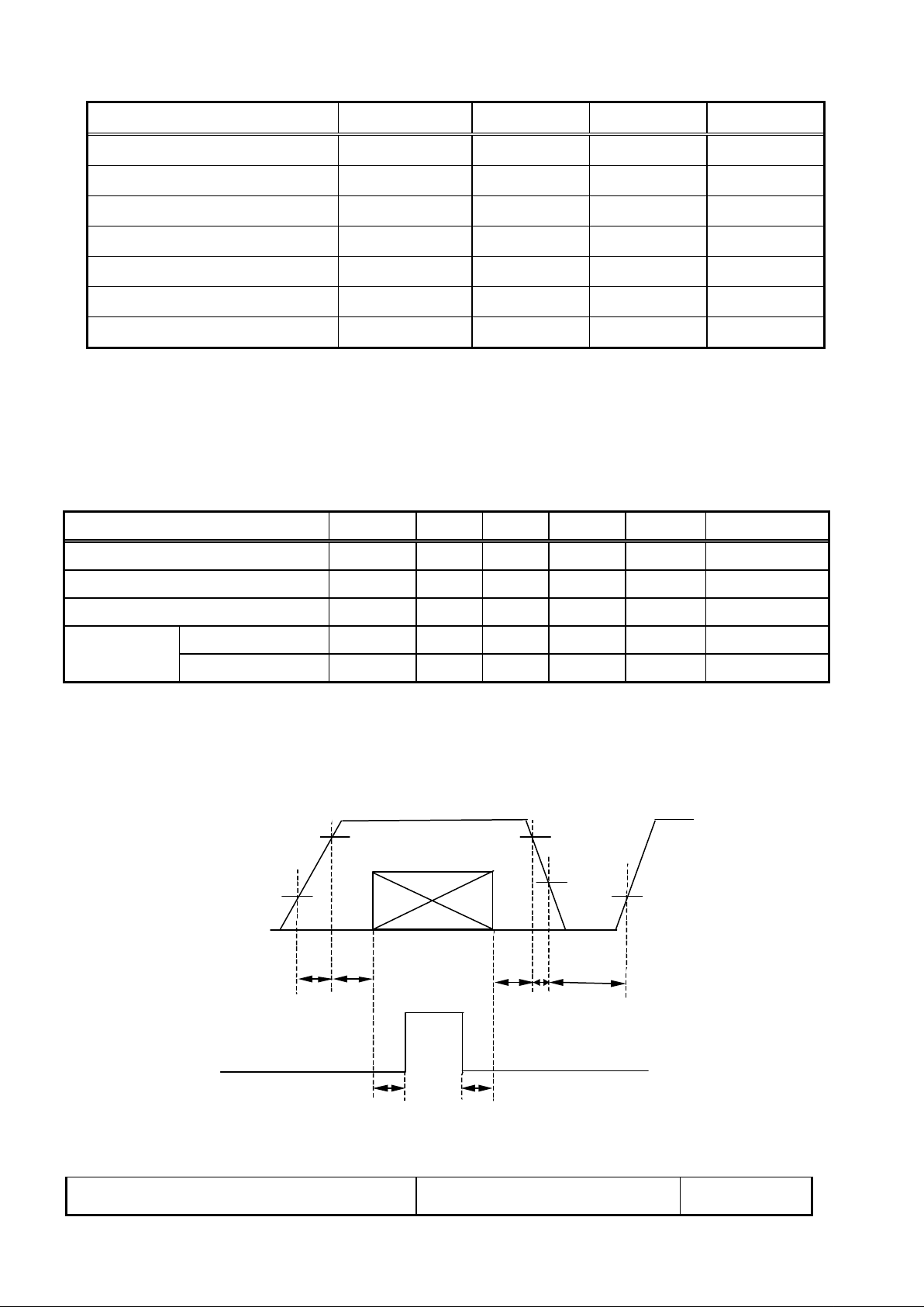
*1) Power and signals sequence:
t1 ≤ 10 ms
0 < t2 ≤ 10 ms
0 < t3 ≤ 1 s
0 < t4 ≤ 50 ms
1 s ≤ t5
200 ms ≤ t6
0 ≤ t7
t1 t2 t3
data
4.5V
4.5V
0.5V
VCC
2.2V
0.5V
t4
t5
LCD Power Supply
Logic Signal
t6 t7
Backlight Power Supply
VL
Data: RGB DATA, DCLK, HD, VD, DENA
T-51511D150-FW-A-AC (AC) No. 2002-0229 OPTREX CORPORATION Page 4/33
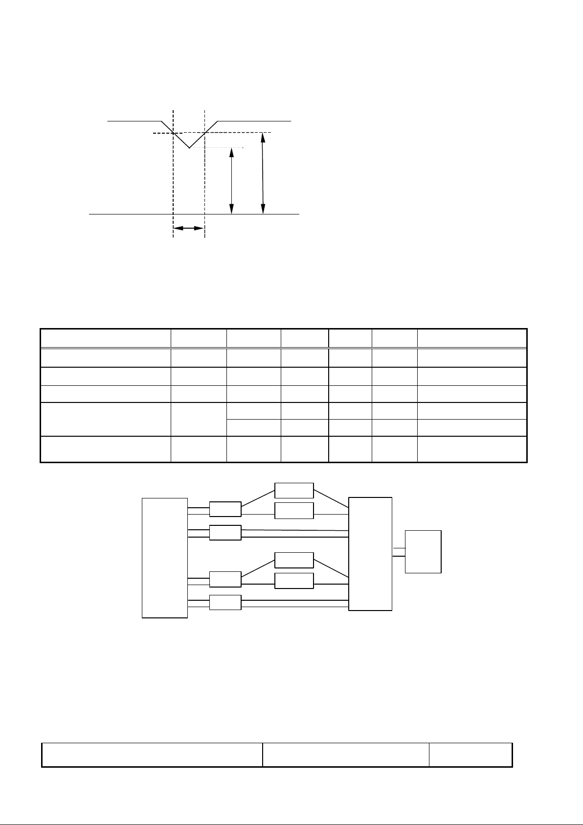
VCC-dip conditions:
1) When VCCMIN ≥ 3.6 V, td ≤ 10 ms
2) When VCCMIN < 3.6 V
VCC-dip conditions should also follow the power and signals sequence.
td
VCCMIN
4.5V
VCC
*2) Typical current condition:
256- gray- bar-pattern
768 line mode
VCC = 5.0 V, fH = 48.4 kHz, fV = 60 Hz, f
CLK
= 32.5 MHz
(2) Backlight Ta = 25°C
ITEM SYMBOL MIN. TYP. MAX. UNIT Remarks
Lamp Voltage VL -- 570 -- Vrms IL = 6.5 mArms
Lamp Current IL 3.5 6.5 8.0 mArms *1)
Lamp Frequency FL 40 -- 70 kHz *2)
1400 -- -- Vrms Ta = 0°C
Starting Lamp Voltage VS
1200
--
--
Vrms Ta = 25°C
Lamp Life Time LT -- 50000 -- h
*3), IL = 6.5 mArms,
Continuous Operation
*1) Lamp Current measurement method (The current meter is inserted in low voltage line.)
CTL
CTL
CTH
CTH
CTL
CTH
CTH
CTL
LCD
Module
A
Inverter
Power
Supply
A
A
A
*2) Lamp frequency of inverter may produce interference with horizontal synchronous frequency,
and this may cause horizontal beat on the display. Therefore, please adjust lamp frequency, and
keep inverter as far from module as possible or use electronic shielding between inverter and
module to avoid the interference.
*3) Lamp life time is defined as the time either when the brightness becomes 50% of the initial value,
or when the starting lamp voltage does not meet the value specified in this table.
T-51511D150-FW-A-AC (AC) No. 2002-0229 OPTREX CORPORATION Page 5/33
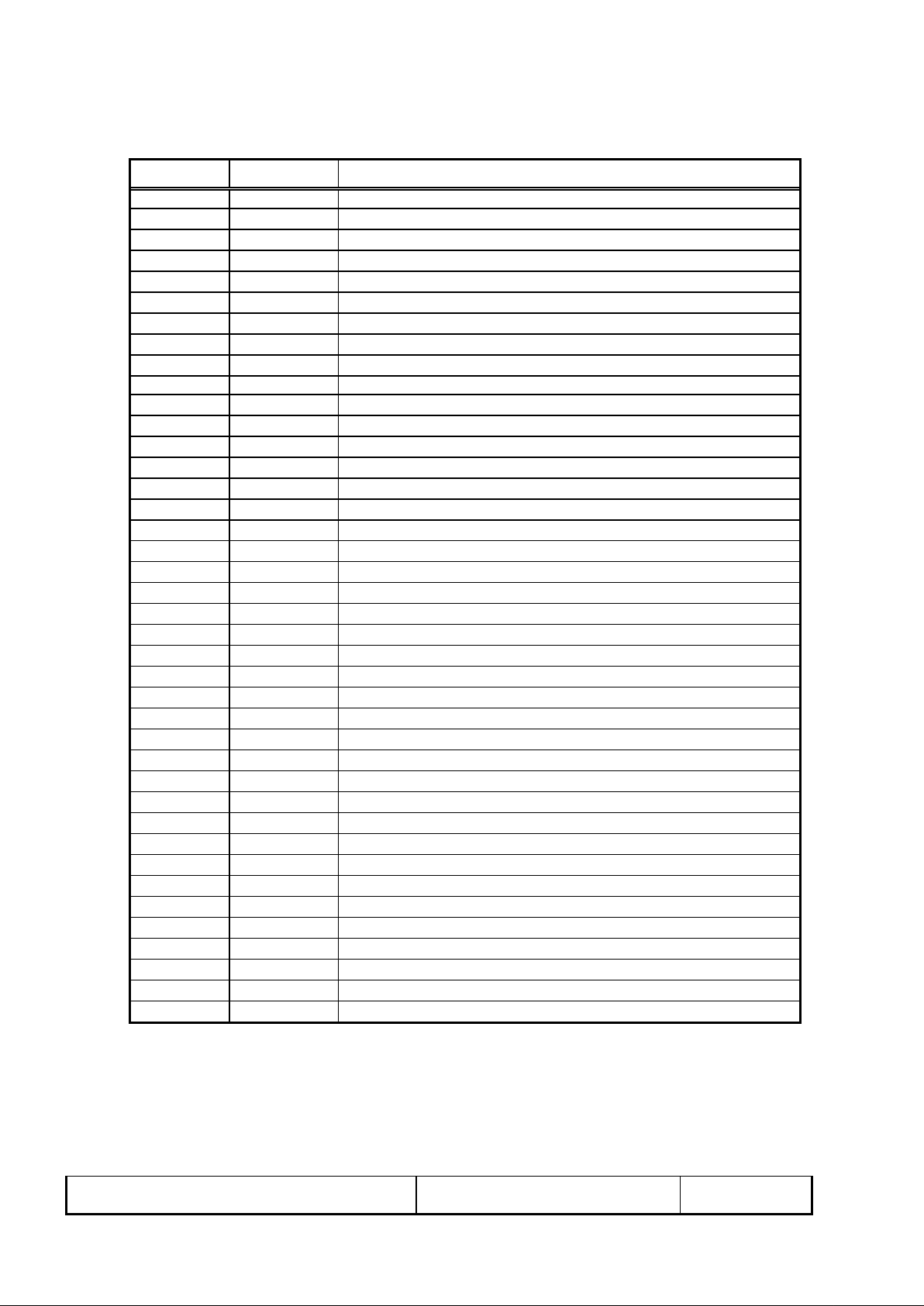
4. INTERFACE PIN CONNECTION
(1) CN 1(Data Signal and Power Supply)
Used Connector: IL-FHR-BF40S-HF (JAE)
Pin No. Symbol Function
1
GND
2 VCC
3 VCC
4 RO0 Red odd data(LSB)
5 RO1 Red odd data
6 RO2 Red odd data
7 RO3 Red odd data
8 GND
9 RO4 Red odd data
10
RO5
Red odd data
11 RO6 Red odd data
12 RO7 Red odd data(MSB)
13 GND
14 GO0 Green odd data(LSB)
15 GO1 Green odd data
16 GO2 Green odd data
17 GO3 Green odd data
18 GND
19 GO4 Green odd data
20 GO5 Green odd data
21 GO6 Green odd data
22 GO7 Green odd data(MSB)
23 GND
24 BO0 Blue odd data(LSB)
25 BO1 Blue odd data
26 BO2 Blue odd data
27 BO3 Blue odd data
28 GND
29 BO4 Blue odd data
30 BO5 Blue odd data
31 BO6 Blue odd data
32 BO7 Blue odd data(MSB)
33 GND
34 NC This pin should be open or GND.
35 HD Horizontal Sync
36 VD Vertical Sync
37 DENA Data enable
38 GND
39 DCLK Dot Clock
40 GND
T-51511D150-FW-A-AC (AC) No. 2002-0229 OPTREX CORPORATION Page 6/33
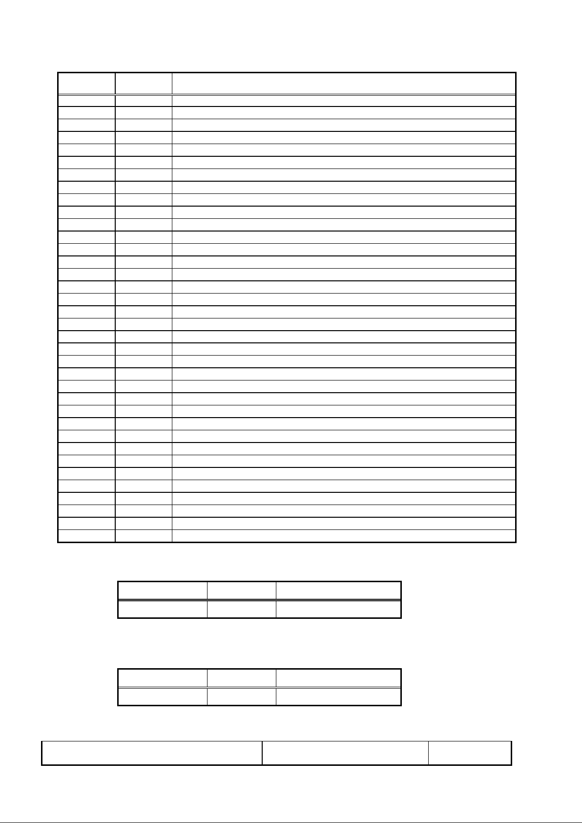
(2) CN 2 (Data signal)
Used Connector: IL-FHR-BF36S-HF (JAE)
Pin No. Symbol Function
1
GND
2
TEST
This pin should be open. Test signal output for only internal test use.
3
TEST
This pin should be open. Test signal output for only internal test use.
4
TEST
This pin should be open. Test signal output for only internal test use.
5
GND
6
GND
7
RE0
Red even data
(LSB)
8
RE1
Red even data
9
RE2
Red even data
10
RE3
Red even data
11
GND
12
RE4
Red even data
13
RE5
Red even data
14
RE6
Red even data
15
RE7
Red even data(MSB)
16
GND
17GE0
Green even data
(LSB)
18GE1
Green even data
19GE2
Green even data
20GE3
Green even data
21
GND
22
GE4
Green even data
23
GE5
Green even data
24
GE6
Green even data
25
GE7
Green even data(MSB)
26
GND
27
BE0
Blue even data
(LSB)
28
BE1
Blue even data
29
BE2
Blue even data
30
BE3
Blue even data
31
GND
32
BE4
Blue even data
33
BE5
Blue even data
34
BE6
Blue even data
35
BE7
Blue even data(MSB)
36
GND
(3) CN 3, 4(Backlight)
Backlight-side connector: BHSR-02VS-1(JST)
Inverter-side connector: SM02B-BHSS-1-TB
Pin No. Symbol Function
1, 2 CTH VBLH(High Voltage)
[Note] VBLH-VBLL = VL
(4) CN 5, 6(Backlight)
Backlight-side connector: BHR-02VS-1(JST)
Inverter-side connector: SM02(4.0)B-BHS-1-TB
Pin No. Symbol Function
1, 2 CTL VBLL(Low Voltage)
[Note] VBLH-VBLL = VL
 Loading...