

Page 1
Global LCD Panel Exchange Center
www.panelook.com
One step solution for LCD / PDP / OLED panel application: Datasheet, inventory and accessory!
www.panelook.com
Prepared by (Module Coordination Group)
First Edition
Aug 22, 2003
LCD Module Technical Specification
Type No.
T-51784D150-FW-A-AA
Approved by (Quality Assurance Division)
Checked by (ACI Engineering Division)
No. Item Page
-- CONTENTS 1
Final Revision
******
1 OVERVIEW 2
2 ABSOLUTE MAXIMUM RATINGS 3
3 ELECTRICAL CHARACTERISTICS 3
4 INTERFACE PIN CONNECTION 6
5 INTERFACE TIMING 8
6 BLOCK DIAGRAM 12
7 MECHANICAL SPECIFICATION 13
8 OPTICAL CHARACTERISTICS 15
9 RELIABILITY TEST CONDITION 18
10 INSPECTION STANDARDS 19
11 HANDLING PRECAUTIONS FOR TFT-LCD MODULE 20
-- PACKAGING SPECIFICATION 23
-- PRODUCT NUMBER LABELING FORMS 27
-- LAMP UNIT FOR 15.0” XGA 29
T-51784D150-FW-A-AA (AA) No. 2003-0143 OPTREX CORPORATION Page 1/35
Page 2
Global LCD Panel Exchange Center
www.panelook.com
One step solution for LCD / PDP / OLED panel application: Datasheet, inventory and accessory!
www.panelook.com
1. OVERVIEW
T-51784D150-FW-A-AA is 15.0” color TFT-LCD (Thin Film Transistor Liquid Crystal Display)
modules composed of LCD panel, driver ICs, control circuit, and backlight unit.
By applying 8bit digital data, 1024 × 768, 16.7M-color images are displayed on the 15.0” diagonal
screen. Input power voltages are 5.0 V for LCD driving.
The type of data and control signals are digital, and 2 pixel data are transmitted per Typ. 32.5 MHz
clock cycle.
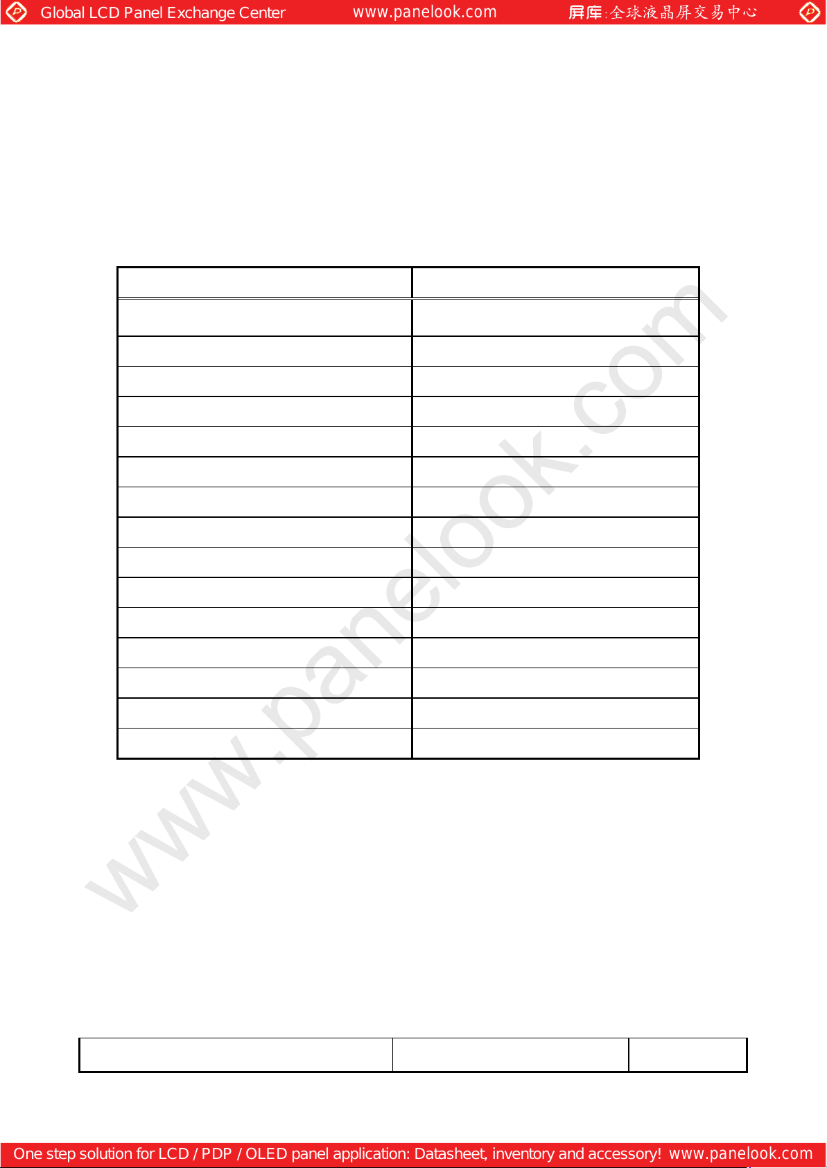
General specifications are summarized in the following table:
ITEM SPECIFICATION
Display Area (mm)
Number of Dots 1024 × 3 (H) × 768 (V)
Pixel Pitch (mm) 0.297 (H) × 0.297 (V)
Color Pixel Arrangement RGB vertical stripe
Display Mode Normally white TN
Number of Color 16.7 M(8 bits/color)
Brightness 450 cd/m2(Typ.)
Wide Viewing Angle Technology Optical Compensation Film
Viewing Angle -75~75° (H) -60~50° (V)
Surface Treatment Anti-glare and hard-coating 3H
Electrical Interface CMOS(VI = 3~5 V, 2 pixel / clock)
Optimum Viewing Angle(Contrast ratio) 6 o’clock
Module Size (mm) 326.0 (W) × 255.0 (H) × 15.9(D)
304.1 (H) × 228.1 (V)
(15.0-inch diagonal)
Module Mass (g) 1350
Backlight Unit CCFL, 4-tubes, edge-light
Characteristic value without any note is typical value.
The LCD product described in this specification is designed and manufactured for the standard use
in OA equipment and consumer products, such as computers, communication equipment, industrial
robots, AV equipment and so on.
Do not use the LCD product for the equipment that require the extreme high level of reliability,
such as aerospace applications, submarine cables, nuclear power control systems and medical or
other equipment for life support.
OPTREX assumes no responsibility for any damage resulting from the use of the LCD product in
disregard of the conditions and handling precautions in this specification.
If customers intend to use the LCD product for the above items or other no standard items,
please contact our sales persons in advance.
T-51784D150-FW-A-AA (AA) No. 2003-0143 OPTREX CORPORATION Page 2/35
Page 3
Global LCD Panel Exchange Center
www.panelook.com
One step solution for LCD / PDP / OLED panel application: Datasheet, inventory and accessory!
www.panelook.com
Logic Signal
Backlight Power Supply
Data: RGB DATA, DCLK, HD, VD, DENA,
2. ABSOLUTE MAXIMUM RATINGS
ITEM SYMBOL MIN. MAX. UNIT
Power Supply Voltage for LCD VCC 0 7.0 V
Logic Input Voltage VI -0.5 6.1 V
Lamp Voltage VL 0 2500 Vrms
Lamp Current IL 0 9.0 mArms
Lamp Frequency FL -- 100 kHz
Operation Temperature *) T
Storage Temperature *) T
op
stg
0 50 °C
-20 60 °C
[Note]
*) Top,Tstg ≤ 40°C : 90% RH max. without condensation
Top,Tstg > 40°C : Absolute humidity shall be less than the value of 90% RH at 40°C without
condensation.
3. ELECTRICAL CHARACTERISTICS
(1) TFT- LCD Ambient Temperature : Ta = 25°C
ITEM SYMBOL MIN. TYP. MAX. UNIT Remarks
Power Supply Voltages for LCD VCC 4.5 5.0 5.5 V *1)
Power Supply Currents for LCD ICC -- 700 900 mA *2)
Permissive Input Ripple Voltage VRP -- -- 100 mVp-p VCC = +5.0 V
Logic Input High VIH 2.2 3.3 5.5 V
Voltage Low VIL 0 -- 0.8 V
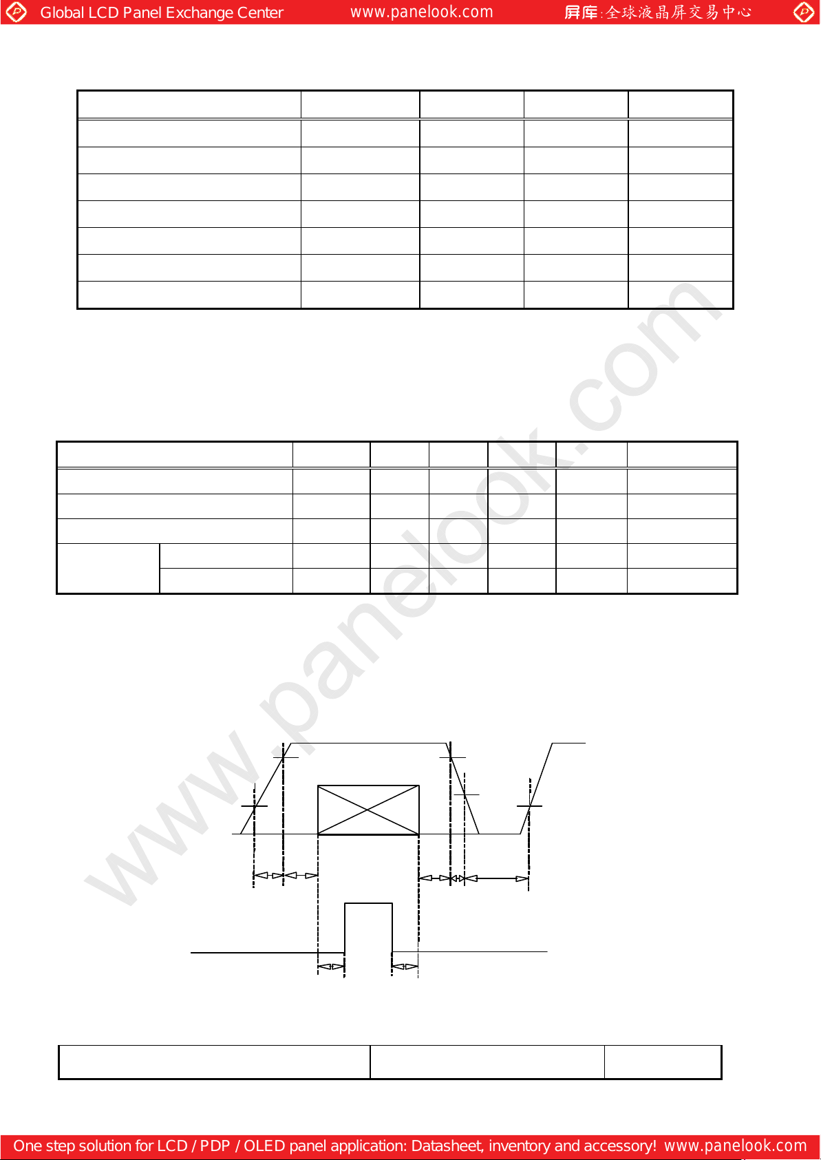
*1) Power and signals sequence:
t1 ≤ 10 ms
0 < t2 ≤ 10 ms
1 s ≤ t5
200 ms ≤ t6
0 < t3 ≤ 1 s
0 ≤ t7
0 < t4 ≤ 50 ms
VCC
4.5V
LCD Power Supply
0.5V
t1 t2 t3
T-51784D150-FW-A-AA (AA) No. 2003-0143 OPTREX CORPORATION Page 3/35
data
VL
t6 t7
4.5V
2.2V
0.5V
t4
t5
Page 4
Global LCD Panel Exchange Center
www.panelook.com
One step solution for LCD / PDP / OLED panel application: Datasheet, inventory and accessory!
www.panelook.com
4.5V
VCC
CTL
VCC-dip conditions:
1) When VCCMIN ≥ 3.6 V, td ≤ 10 ms
2) When VCCMIN < 3.6 V
VCC-dip conditions should also follow the power and signals sequence.
td
*2) Typical current condition:
256- gray- bar-pattern
768 line mode
VCC = 5.0 V, fH = 48.4 kHz, fV = 60 Hz, f
VCCMIN
CLK
= 32.5 MHz
(2) Backlight Ta = 25°C
ITEM SYMBOL MIN. TYP. MAX. UNIT Remarks
Lamp Voltage VL -- 595 -- Vrms IL = 6.5 mArms
Lamp Current IL 3.5 6.5 7.0 mArms *1), *4)
Lamp Frequency FL 40 -- 70 kHz *2)
1350 -- -- Vrms Ta = 0°C
Starting Lamp Voltage VS
1000
--
--
Lamp Life Time LT -- 50000 -- h
Vrms Ta = 25°C
*3), IL = 6.5 mArms,
Continuous Operation
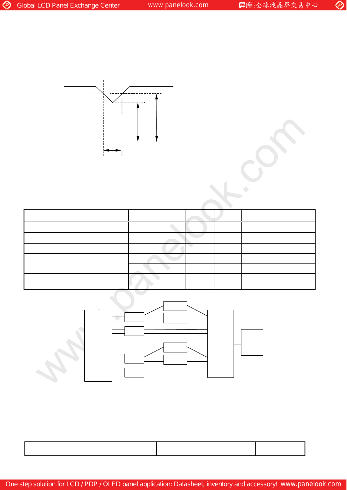
*1) Lamp Current measurement method (The current meter is inserted in low voltage line.)
A
A
A
Inverter
A
Power
Supply
LCD
Module
CTL
CTL
CTH
CTH
CTL
CTH
CTH
*2) Lamp frequency of inverter may produce interference with horizontal synchronous frequency,
and this may cause horizontal beat on the display. Therefore, please adjust lamp frequency, and
keep inverter as far from module as possible or use electronic shielding between inverter and
module to avoid the interference.
*3) Lamp life time is defined as the time either when the brightness becomes 50% of the initial value,
or when the starting lamp voltage does not meet the value specified in this table.
T-51784D150-FW-A-AA (AA) No. 2003-0143 OPTREX CORPORATION Page 4/35
Page 5
Global LCD Panel Exchange Center
www.panelook.com
One step solution for LCD / PDP / OLED panel application: Datasheet, inventory and accessory!
www.panelook.com
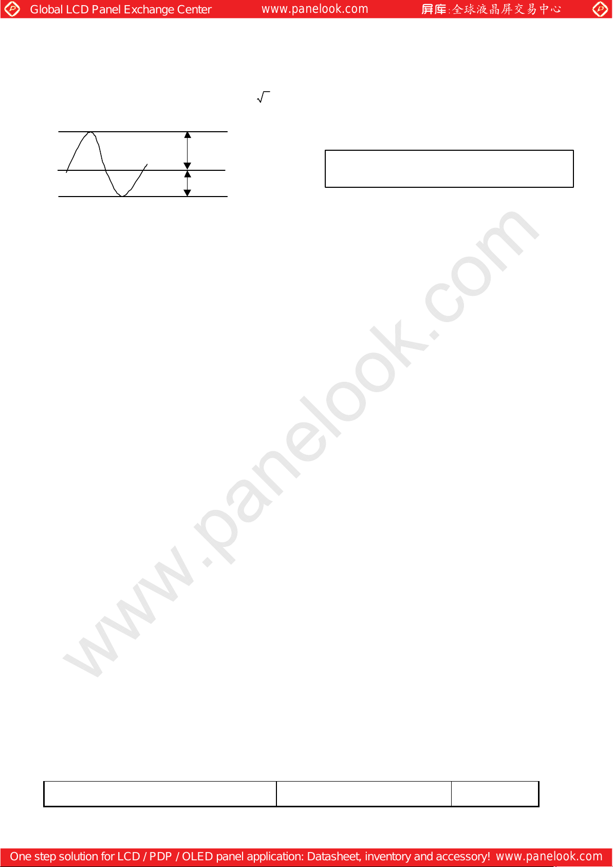
*4) Please use the inverter which has symmetrical current wave form as follows,
The degree of unbalance: less than 10%
The ratio of wave height: less than 2±10%
I
PH
I
PL
IPH: High side peak
The degree of unbalance = |IPH - IPL| / Irms
The ratio of wave height = IPH(or IPL) / Irms
IPL: Low side peak
CURRENT WAVE FORM
×
100(%)
T-51784D150-FW-A-AA (AA) No. 2003-0143 OPTREX CORPORATION Page 5/35
Page 6
Global LCD Panel Exchange Center
www.panelook.com
One step solution for LCD / PDP / OLED panel application: Datasheet, inventory and accessory!
www.panelook.com
1
GND
10
RO5
Red odd data
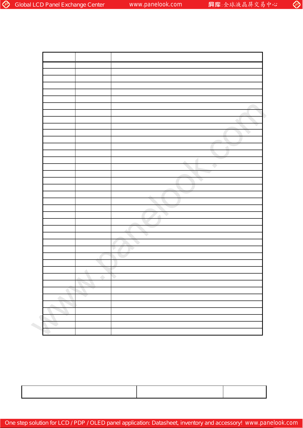
4. INTERFACE PIN CONNECTION
(1) CN 1(Data Signal and Power Supply)
Used Connector: IL-FHR-BF40S-HF (JAE)
Pin No. Symbol Function
2 VCC
3 VCC
4 RO0 Red odd data(LSB)
5 RO1 Red odd data
6 RO2 Red odd data
7 RO3 Red odd data
8 GND
9 RO4 Red odd data
11 RO6 Red odd data
12 RO7 Red odd data(MSB)
13 GND
14 GO0 Green odd data(LSB)
15 GO1 Green odd data
16 GO2 Green odd data
17 GO3 Green odd data
18 GND
19 GO4 Green odd data
20 GO5 Green odd data
21 GO6 Green odd data
22 GO7 Green odd data(MSB)
23 GND
24 BO0 Blue odd data(LSB)
25 BO1 Blue odd data
26 BO2 Blue odd data
27 BO3 Blue odd data
28 GND
29 BO4 Blue odd data
30 BO5 Blue odd data
31 BO6 Blue odd data
32 BO7 Blue odd data(MSB)
33 GND
34 NC This pin should be open.
35 HD Horizontal Sync
36 VD Vertical Sync
37 DENA Data enable
38 GND
39 DCLK Dot Clock
40 GND
T-51784D150-FW-A-AA (AA) No. 2003-0143 OPTREX CORPORATION Page 6/35
Page 7
Global LCD Panel Exchange Center
www.panelook.com
One step solution for LCD / PDP / OLED panel application: Datasheet, inventory and accessory!
www.panelook.com
1
GND
2
TEST
This pin should be open. Test signal output for only internal test use.
3
TEST
This pin should be open. Test signal output for only internal test use.
4
TEST
This pin should be open. Test signal output for only internal test use.
5
GND
6
GND
7
RE0
Red even data(LSB)
8
RE1
Red even data
9
RE2
Red even data
10
RE3
Red even data
11
GND
12
RE4
Red even data
13
RE5
Red even data
14
RE6
Red even data
15
RE7
Red even data(MSB)
16
GND
17
GE0
Green even data(LSB)
18
GE1
Green even data
19
GE2
Green even data
20
GE3
Green even data
21
GND
22
GE4
Green even data
23
GE5
Green even data
24
GE6
Green even data
25
GE7
Green even data(MSB)
26
GND
27
BE0
Blue even data(LSB)
28
BE1
Blue even data
29
BE2
Blue even data
30
BE3
Blue even data
31
GND
32
BE4
Blue even data
33
BE5
Blue even data
34
BE6
Blue even data
35
BE7
Blue even data(MSB)
36
GND
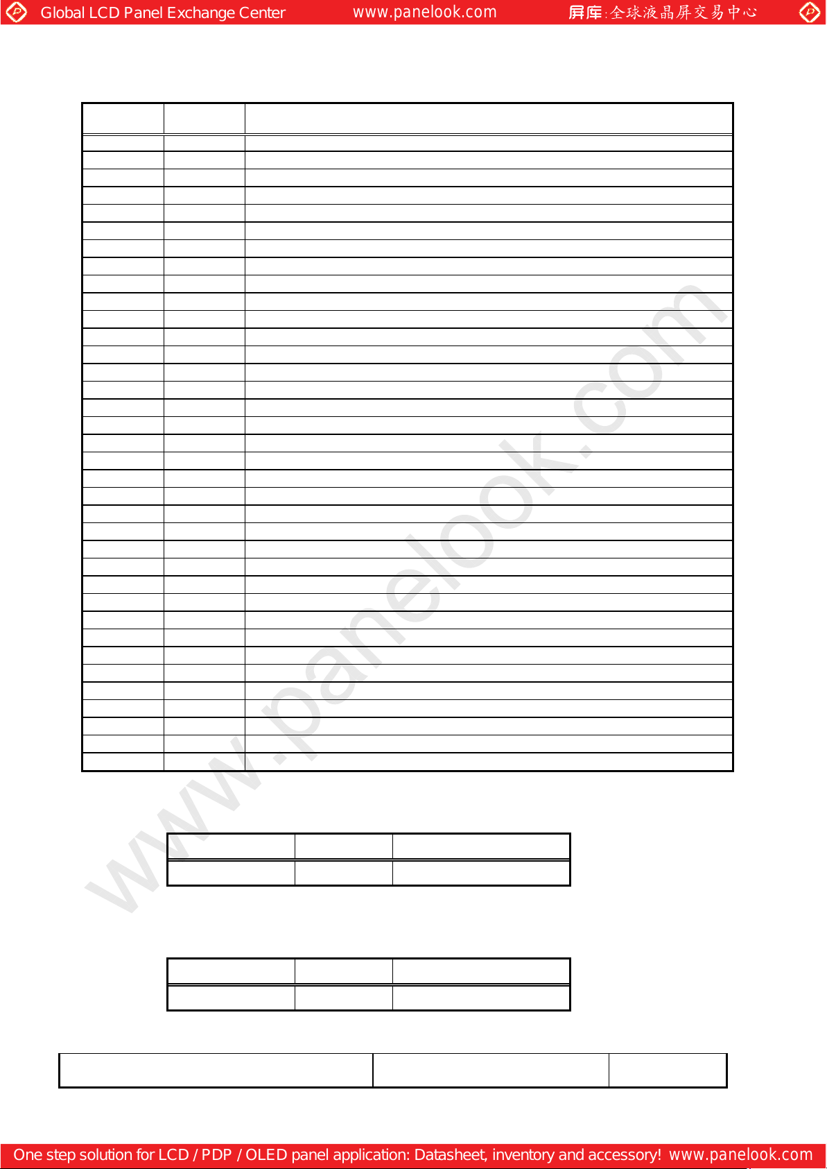
(2) CN 2 (Data signal)
Used Connector: IL-FHR-BF36S-HF (JAE)
Pin No. Symbol Function
(3) CN 3, 4(Backlight)
Backlight-side connector: BHSR-02VS-1(JST)
Inverter-side connector: SM02B-BHSS-1-TB
Pin No. Symbol Function
1, 2 CTH VBLH(High Voltage)
[Note] VBLH-VBLL = VL
(4) CN 5, 6(Backlight)
Backlight-side connector: BHR-02VS-1(JST)
Inverter-side connector: SM02(4.0)B-BHS-1-TB
Pin No. Symbol Function
1, 2 CTL VBLL(Low Voltage)
[Note] VBLH-VBLL = VL
T-51784D150-FW-A-AA (AA) No. 2003-0143 OPTREX CORPORATION Page 7/35
Page 8
Global LCD Panel Exchange Center
www.panelook.com
One step solution for LCD / PDP / OLED panel application: Datasheet, inventory and accessory!
www.panelook.com
5. INTERFACE TIMING
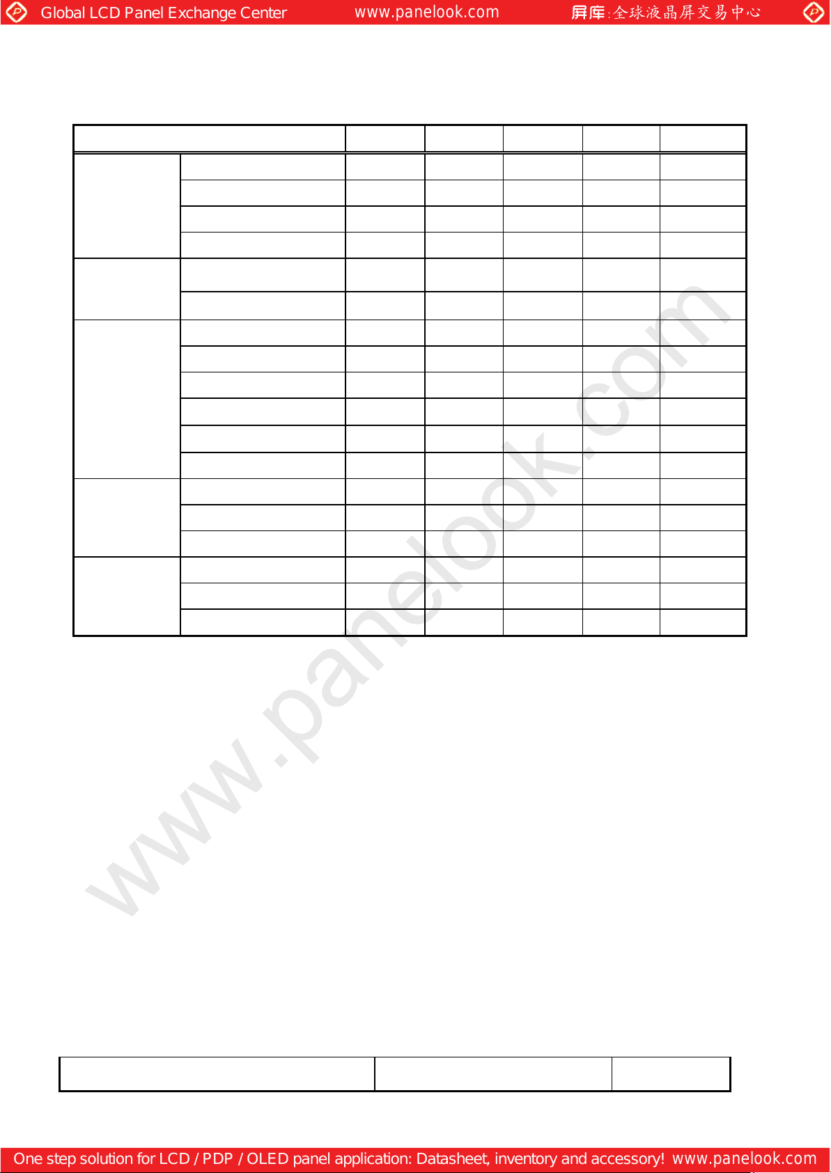
(1) Timing Specifications
ITEM SYMBOL MIN. TYP. MAX. UNIT
DCLK
*1) *4)
DATA *1)
(R,G,B,DENA,
HD, VD)
DENA
*3)
HD
*2)*4)
Frequency f
Period t
Low Width t
High Width t
Set up time t
Hold time t
Horizontal Active Time t
Horizontal Front Porch t
Horizontal Back Porch t
Vertical Active Time t
Vertical Front Porch t
Vertical Back Porch t
Frequency f
Period t
Low Width t
Frequency f
CLK
CLK
WCL
WCH
DS
DH
HA
HFP
HBP
VA
VFP
VBP
H
H
WHL
V
30 32.5 40 MHz
25.0 30.8 33.3 ns
5 -- -- ns
5 -- -- ns
3 -- -- ns
6 -- -- ns
512 512 512 t
16 24 -- t
28 33 -- t
CLK
CLK
CLK
768 768 768 t
2 3 -- t
4 35 -- t
-- 48.4 62.5 kHz
16 20.7 -- µs
4 8 -- t
CLK
55 60 75 Hz
H
H
H
Period t
Low Width t
V
WVL
13.3 16.7 18.2 msVD *2)
2 6 -- t
[Note]
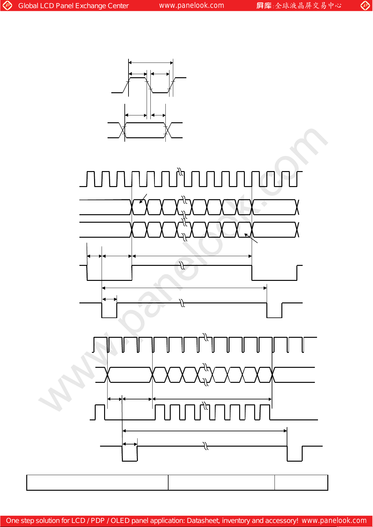
*1) DATA is latched at fall edge of DCLK in this specification.
*2) Polarities of HD and VD are negative in this specification.
*3) DENA (Data Enable) should always be positive polarity as shown in the timing specification.
*4) DCLK should appear during all invalid period, and HD should appear during invalid period of
frame cycle.
H
T-51784D150-FW-A-AA (AA) No. 2003-0143 OPTREX CORPORATION Page 8/35
Page 9
Global LCD Panel Exchange Center
www.panelook.com
One step solution for LCD / PDP / OLED panel application: Datasheet, inventory and accessory!
www.panelook.com
2.2V
0.8V
0.8V
2.2V
Last Data
VD
HD
(2) Timing Chart
a. Pixel Timing Chart
DCLK
DATA
(R,G,B,ODD,EVEN),
DENA, HD, VD
b. Horizontal Timing Chart
DCLK
ODD DATA
(R,G,B)
EVEN DATA
(R,G,B)
Invalid Data
Invalid Data
t
CLK
tWCH tWCL
DS
123
t
DH
4
t
1021
1022
1023
1024
Invalid Data
Invalid Data
5
6
t
HFP
t
HBP
DENA
t
WHL
HD
c. Vertical Timing Chart
LINE DATA
t
VFP
DENA
tVBP
t
HA
tH=1/f
H
1 2 767 7683Invalid Data Invalid Data
tVA
tV=1/fV
t
WVL
T-51784D150-FW-A-AA (AA) No. 2003-0143 OPTREX CORPORATION Page 9/35
Page 10
Global LCD Panel Exchange Center
www.panelook.com
One step solution for LCD / PDP / OLED panel application: Datasheet, inventory and accessory!
www.panelook.com
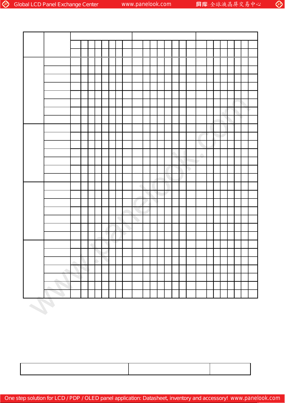
(3) Color Data Assignment
R DATA G DATA B DATA
COLOR R7 R6 R5 R4 R3 R2 R1 R0 G7 G6 G5 G4 G3 G2 G1 G0 B7 B6 B5 B4 B3 B2 B1 B0
INPUT
DATA
MSB LSB MSB LSB MSB LSB
BASIC
COLOR
RED
GREEN
BLACK
RED(255)
GREEN(255)
BLUE(255)
CYAN
MAGENTA
YELLOW
WHITE
RED(0)
RED(1)
RED(2)
RED(254)
RED(255)
GREEN(0)
GREEN(1)
GREEN(2)
0 0 0 0 0 0 0 0 0 0 0 0 0 0 0 0 0 0 0 0 0 0 0 0
1 1 1 1 1 1 1 1 0 0 0 0 0 0 0 0 0 0 0 0 0 0 0 0
0 0 0 0 0 0 0 0 1 1 1 1 1 1 1 1 0 0 0 0 0 0 0 0
0 0 0 0 0 0 0 0 0 0 0 0 0 0 0 0 1 1 1 1 1 1 1 1
0 0 0 0 0 0 0 0 1 1 1 1 1 1 1 1 1 1 1 1 1 1 1 1
1 1 1 1 1 1 1 1 0 0 0 0 0 0 0 0 1 1 1 1 1 1 1 1
1 1 1 1 1 1 1 1 1 1 1 1 1 1 1 1 0 0 0 0 0 0 0 0
1 1 1 1 1 1 1 1 1 1 1 1 1 1 1 1 1 1 1 1 1 1 1 1
0 0 0 0 0 0 0 0 0 0 0 0 0 0 0 0 0 0 0 0 0 0 0 0
0 0 0 0 0 0 0 1 0 0 0 0 0 0 0 0 0 0 0 0 0 0 0 0
0 0 0 0 0 0 1 0 0 0 0 0 0 0 0 0 0 0 0 0 0 0 0 0
1 1 1 1 1 1 1 0 0 0 0 0 0 0 0 0 0 0 0 0 0 0 0 0
1 1 1 1 1 1 1 1 0 0 0 0 0 0 0 0 0 0 0 0 0 0 0 0
0 0 0 0 0 0 0 0 0 0 0 0 0 0 0 0 0 0 0 0 0 0 0 0
0 0 0 0 0 0 0 0 0 0 0 0 0 0 0 1 0 0 0 0 0 0 0 0
0 0 0 0 0 0 0 0 0 0 0 0 0 0 1 0 0 0 0 0 0 0 0 0
GREEN(254)
GREEN(255)
BLUE(0)
BLUE(1)
BLUE(2)
BLUE
BLUE(254)
BLUE(255)
[Note]
*1) Definition of gray scale
Color (n) --- n indicates gray scale level.
*2) Data
1:High, 0: Low
0 0 0 0 0 0 0 0 1 1 1 1 1 1 1 0 0 0 0 0 0 0 0 0
0 0 0 0 0 0 0 0 1 1 1 1 1 1 1 1 0 0 0 0 0 0 0 0
0 0 0 0 0 0 0 0 0 0 0 0 0 0 0 0 0 0 0 0 0 0 0 0
0 0 0 0 0 0 0 0 0 0 0 0 0 0 0 0 0 0 0 0 0 0 0 1
0 0 0 0 0 0 0 0 0 0 0 0 0 0 0 0 0 0 0 0 0 0 1 0
0 0 0 0 0 0 0 0 0 0 0 0 0 0 0 0 1 1 1 1 1 1 1 0
0 0 0 0 0 0 0 0 0 0 0 0 0 0 0 0 1 1 1 1 1 1 1 1
Higher n means brighter level.
T-51784D150-FW-A-AA (AA) No. 2003-0143 OPTREX CORPORATION Page 10/35
Page 11
Global LCD Panel Exchange Center
www.panelook.com
One step solution for LCD / PDP / OLED panel application: Datasheet, inventory and accessory!
www.panelook.com
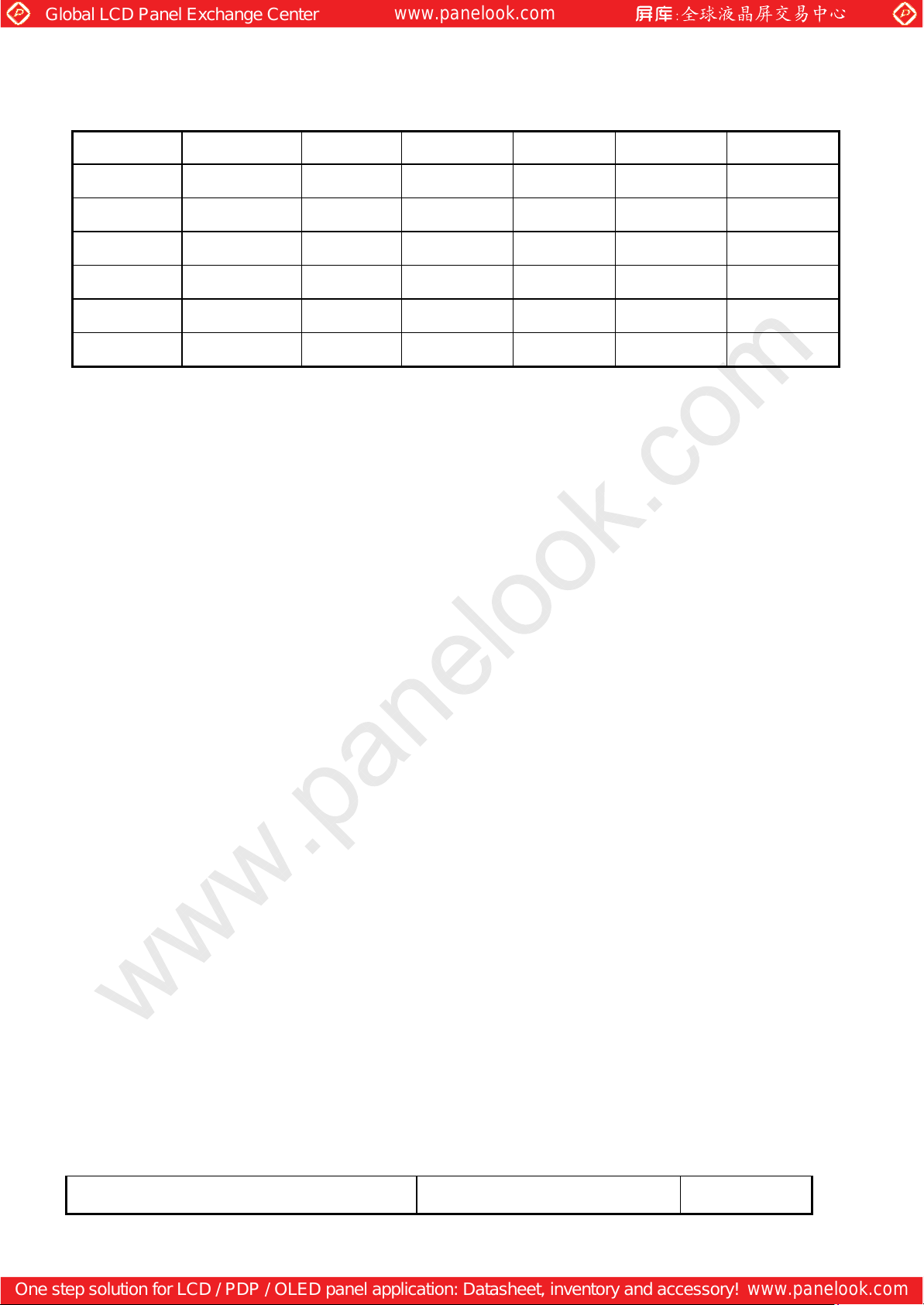
(4) Data Mapping
D( 1, 1) D( 2, 1) --- D( X, 1) --- D(1023, 1) D(1024, 1)
D( 1, 2) D( 2, 2) --- D( X, 2) --- D(1023, 2) D(1024, 2)
¦ ¦ + ¦ + ¦ ¦
D( 1, Y) D( 2, Y) --- D( X, Y) --- D(1023, Y) D(1024, Y)
¦ ¦ + ¦ + ¦ ¦
D( 1,767) D( 2,767) --- D( X,767) --- D(1023,767) D(1024,767)
D( 1,768) D( 2,768) --- D( X,768) --- D(1023,768) D(1024,768)
T-51784D150-FW-A-AA (AA) No. 2003-0143 OPTREX CORPORATION Page 11/35
Page 12
Global LCD Panel Exchange Center
www.panelook.com
One step solution for LCD / PDP / OLED panel application: Datasheet, inventory and accessory!
www.panelook.com
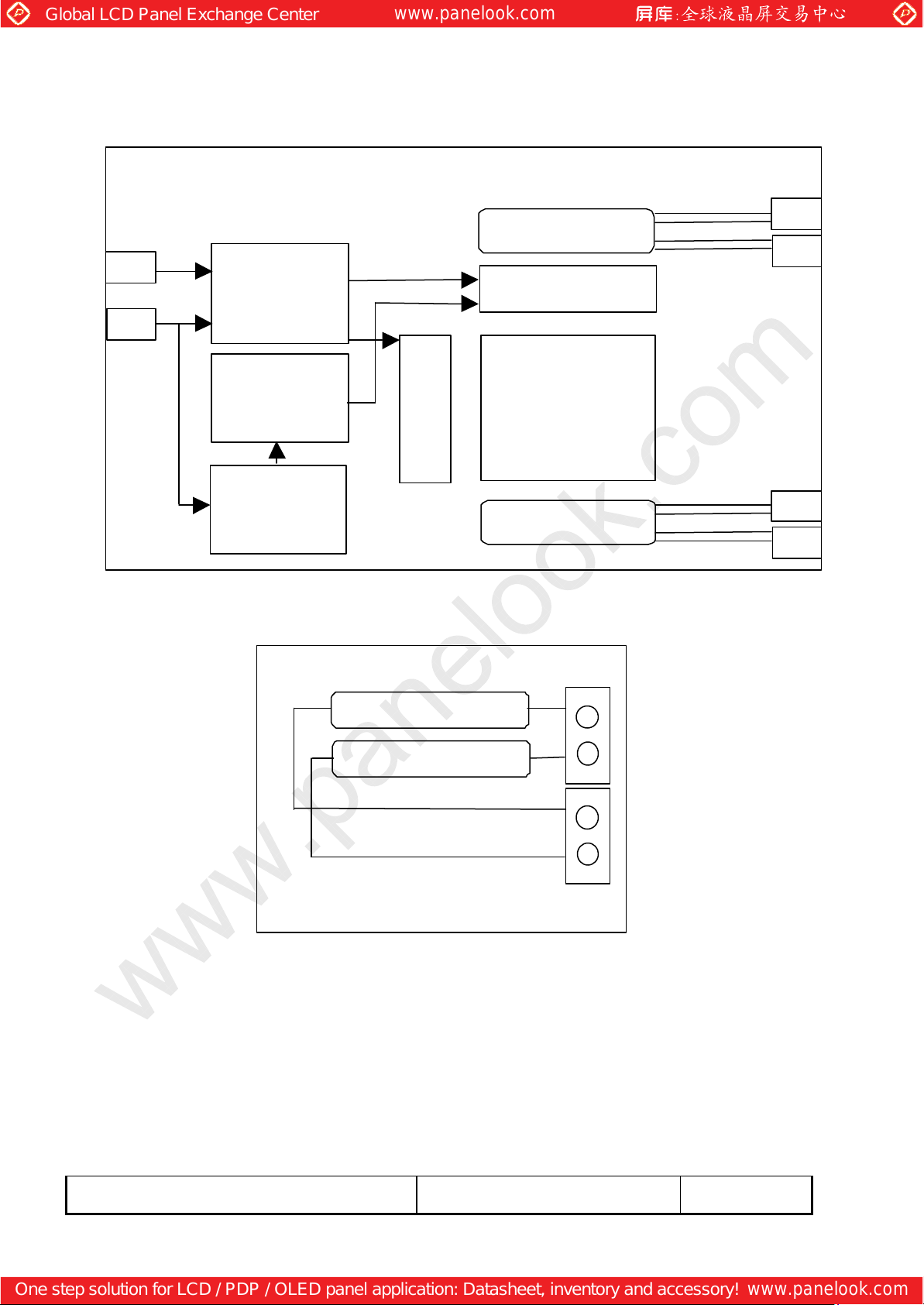
6. BLOCK DIAGRAM
TFT-LCD Module
c
CN2
CN1
Timing
Controller
CN3
Backlight
CN5
Source Driver
Voltage Supply
for Gray Levels
and Vcom
DC/DC
Converter
BACKLIGHT
Gate Driver
CCFL
LCD Panel
1024 X 3 X 768
CN4
Backlight
CN6
CN3, 4
1
2
1
2
CN5, 6
T-51784D150-FW-A-AA (AA) No. 2003-0143 OPTREX CORPORATION Page 12/35
Page 13
Global LCD Panel Exchange Center
www.panelook.com
One step solution for LCD / PDP / OLED panel application: Datasheet, inventory and accessory!
www.panelook.com
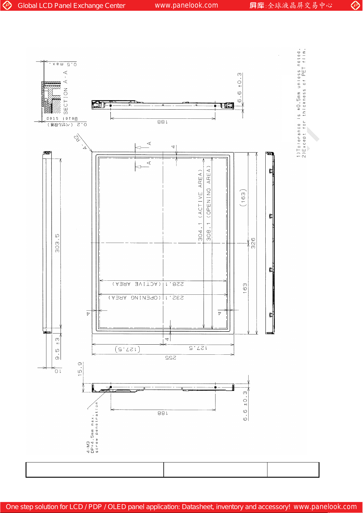
7. MECHANICAL SPECIFICATIONS
(1)Front side
T-51784D150-FW-A-AA (AA) No. 2003-0143 OPTREX CORPORATION Page 13/35
Page 14
Global LCD Panel Exchange Center
www.panelook.com
One step solution for LCD / PDP / OLED panel application: Datasheet, inventory and accessory!
www.panelook.com
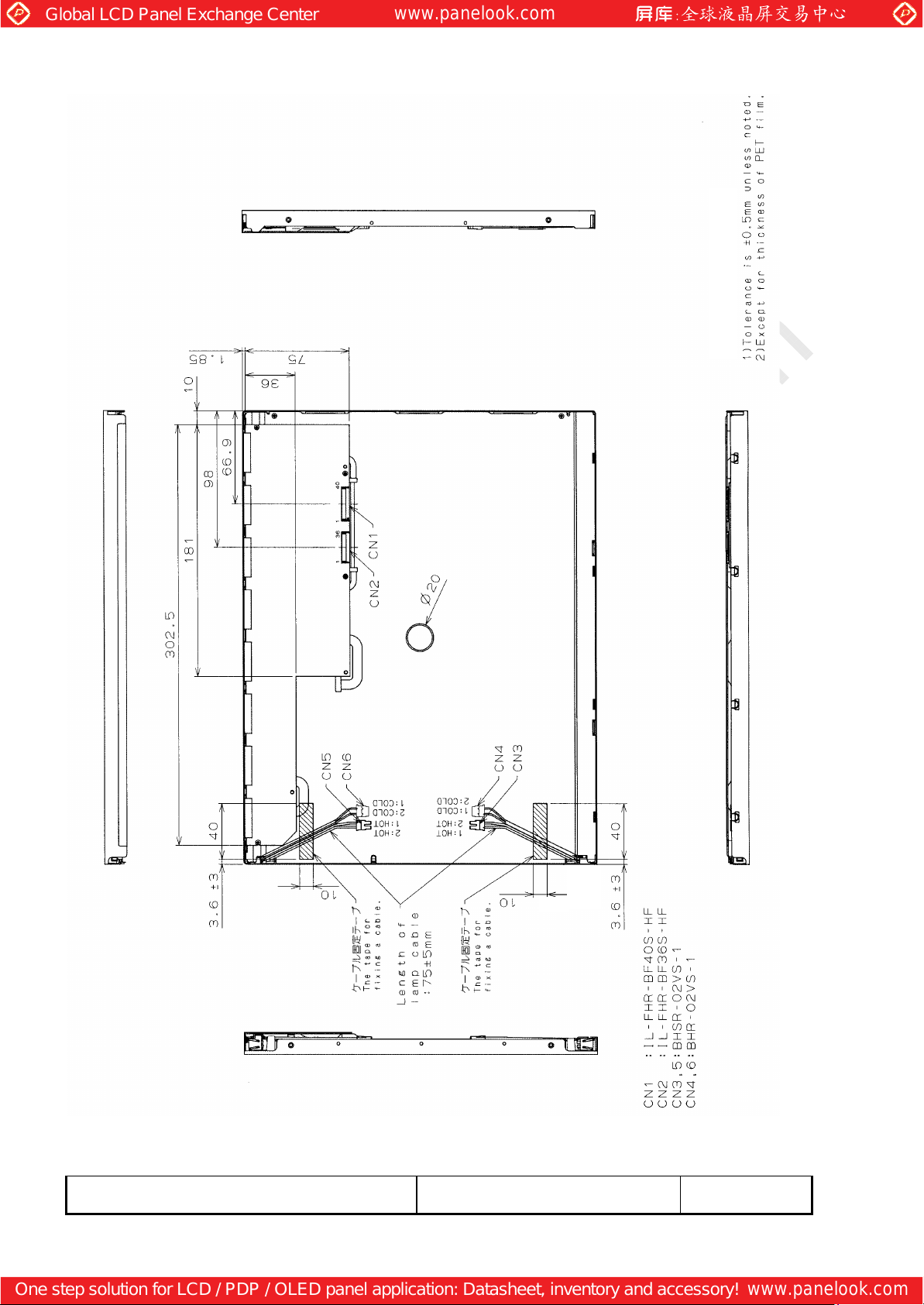
(2)Rear side
[Note] We recommend you referring to the detailed drawing for your design.
Please contact our company sales representative when you need the detailed drawing.
T-51784D150-FW-A-AA (AA) No. 2003-0143 OPTREX CORPORATION Page 14/35
Page 15
Global LCD Panel Exchange Center
www.panelook.com
One step solution for LCD / PDP / OLED panel application: Datasheet, inventory and accessory!
www.panelook.com
768
8. OPTICAL CHARACTERISTICS
Ta = 25°C, VCC = 5.0 V, Input Signals: Typ. Values shown in Section 5
ITEM SYMBOL CONDITION MIN. TYP. MAX. UNIT Remarks
Contrast Ratio CR θ = φ = 0° 350 500 - Luminance Normal Lw θ = φ = 0° 360 450 --
Uniformity ∆Lw θ = φ = 0° -- -- 30
Response Time
(White - Black)
Response Time
(Gray Scale Level)
Horizontal φ CR ≥ 10 -- -75∼75 --
tr θ = φ = 0° -- 6 -- ms *3)*4)
tf θ = φ = 0° -- 19 -- ms *3)*4)
trg,tfg θ = φ = 0° -- 10 15 ms *3)*5)
Viewing Vertical θ -- -60∼50 --
Angle Horizontal φ CR ≥ 5 -- -80∼80 --
Vertical θ -- -80∼70 --
Image Sticking tis 2 h -- -- 2 s
Red Rx 0.607 0.637 0.667
Ry 0.297 0.327 0.357
Color Green Gx 0.243 0.273 0.303
Coordinates Gy θ = φ = 0° 0.553 0.583 0.613
Blue Bx 0.112 0.142 0.172
By 0.022 0.052 0.082
White Wx 0.253 0.283 0.313
Wy 0.267 0.297 0.327
[Note]
These items are measured using CS1000(MINOLTA) for color coordinates, EZContrast(ELDIM) for
viewing angle, and CS1000 or BM-5A(TOPCON) for others under the dark room condition (no ambient
light) after more than 30 minutes from turning on the lamp unless noted.
--
cd/m
%
°
°
°
°
--
2
*1)*3)
*2)*3)
*2)*3)
*3)
*3)
*3)
*3)
*6)
*3)
Condition: IL = 6.5 mArms, Inverter frequency: 60 kHz
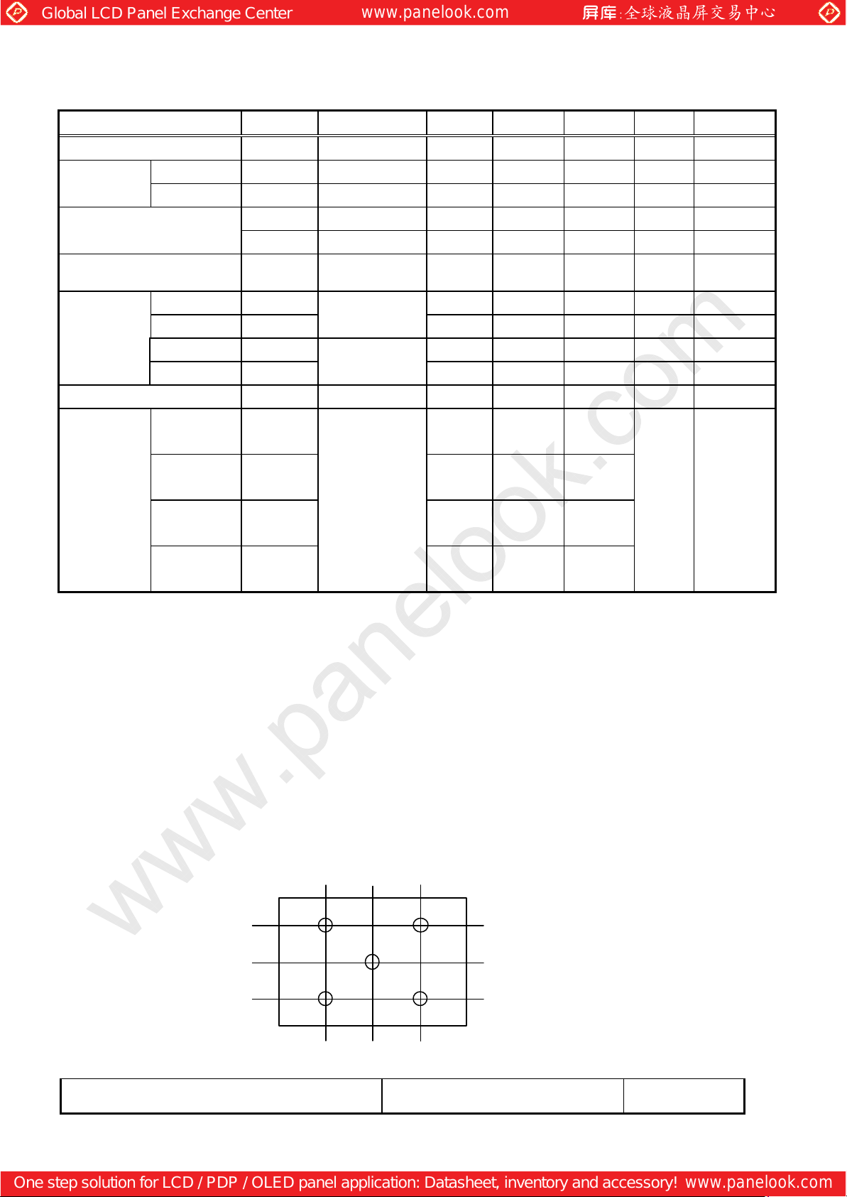
*1) Definition of Contrast Ratio
CR=ON(White) Luminance / OFF(Black) Luminance: the center of 5 points (No.5) shown in a
figure below
*2) Definition of Luminance and Luminance Uniformity
Lw=ON (White) Luminance: the center of 5 points (No.5) shown in a figure below
∆Lw=[Lw(MAX)/Lw(MIN)-1] × 100: Measure Contrast ratio and White Luminance on the below 5
points
(1,1)
192
384
576
256 512
1
3
2
5
4
(1024,768)
MEASUREMENT POINT
T-51784D150-FW-A-AA (AA) No. 2003-0143 OPTREX CORPORATION Page 15/35
Page 16
Global LCD Panel Exchange Center
www.panelook.com
One step solution for LCD / PDP / OLED panel application: Datasheet, inventory and accessory!
www.panelook.com
Luminance
tft
r
Luminance
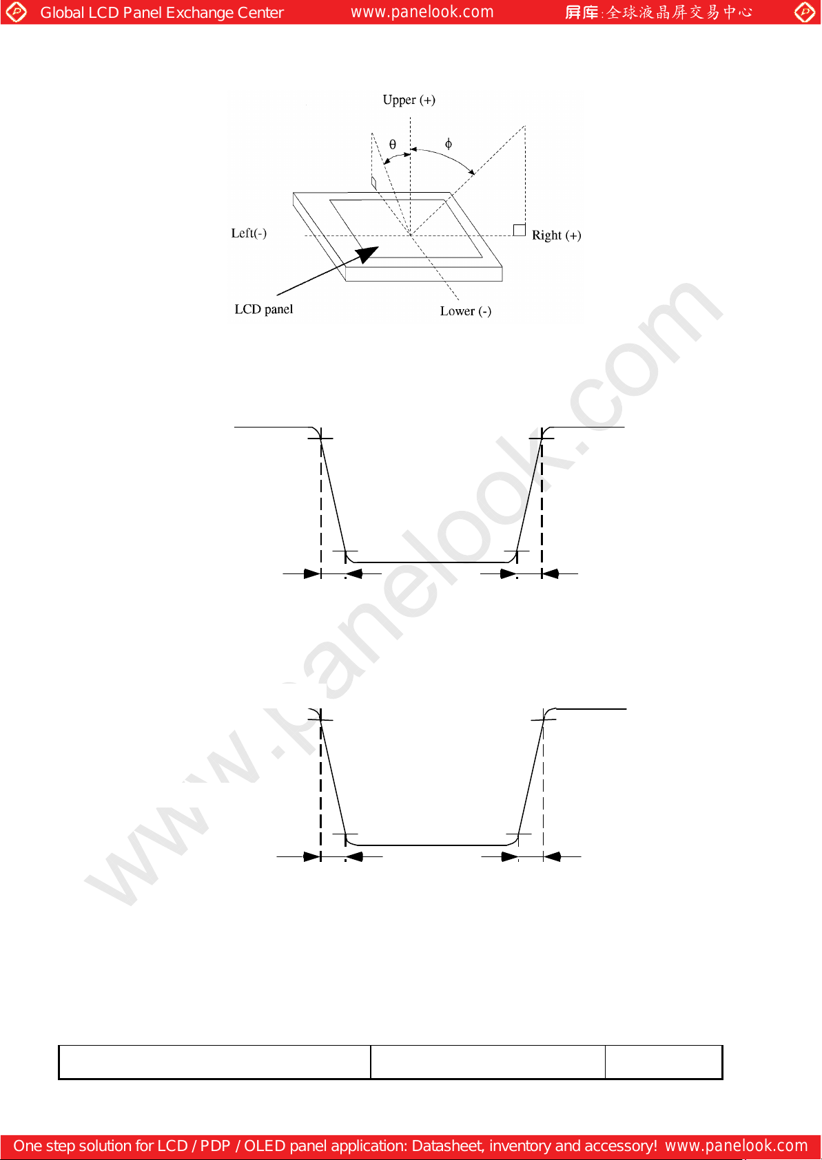
*3) Definition of Viewing Angle( θ , φ)
*4) Definition of Response Time (White - Black)
White(255th)
90%90%
10%
*5) Definition of Response Time(Gray Scale Level between 32th and 224th at intervals of 32 levels)
(64~224th)
(Gray Scale Level)
10%
Black(0)
90%90%
trg
T-51784D150-FW-A-AA (AA) No. 2003-0143 OPTREX CORPORATION Page 16/35
10%
10%
(32~192th)
tfg
Page 17
Global LCD Panel Exchange Center
www.panelook.com
One step solution for LCD / PDP / OLED panel application: Datasheet, inventory and accessory!
www.panelook.com
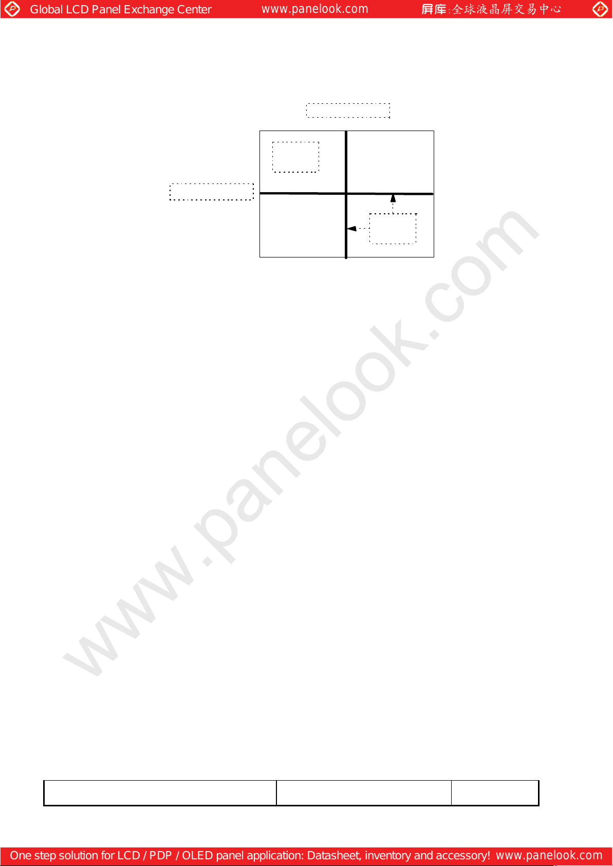
Cols 510-514
*6) Image Sticking
Continuously display the test pattern shown in the figure below for two-hours. Then display a
completely white screen. The previous image shall not persist more than two seconds at 25°C.
Rows 382-386
TEST PATTERN FOR IMAGE STICKING TEST
White
Area
Black
Lines
T-51784D150-FW-A-AA (AA) No. 2003-0143 OPTREX CORPORATION Page 17/35
Page 18
Global LCD Panel Exchange Center
www.panelook.com
One step solution for LCD / PDP / OLED panel application: Datasheet, inventory and accessory!
www.panelook.com
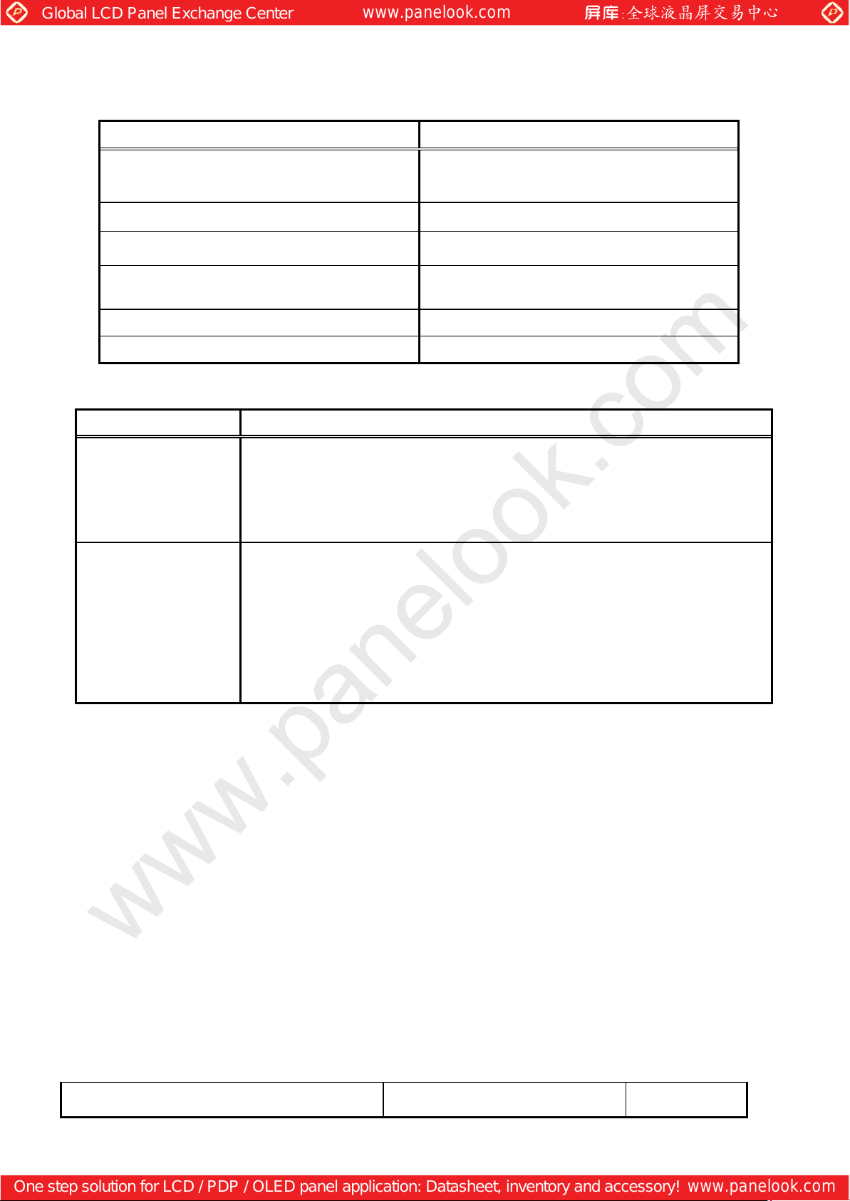
9. RELIABILITY TEST CONDITION
(1) Temperature and Humidity
TEST ITEM CONDITIONS
HIGH TEMPERATURE 40°C, 90% RH, 240h
HIGH HUMIDITY OPERATION (No condensation)
HIGH TEMPERATURE OPERATION 50°C, 240 h
LOW TEMPERATURE OPERATION 0°C, 240 h
THERMAL SHOCK
(Non-Operation)
HIGH TEMPERATURE STORAGE 60°C, 240 h
LOW TEMPERATURE STORAGE -20°C, 240 h
(2) Shock & Vibration
ITEM CONDITIONS
Shock level: 980 m/s2 (100 G)
SHOCK Waveform: half sinusoidal wave, 2 ms
(NON-OPERATION) Number of shocks: one shock input in each direction of three mutually
Perpendicular axes for a total of six shock inputs
Vibration level: 9.8 m/s2 (1.0 G)zero to peak
Waveform: sinusoidal
VIBRATION Frequency range: 5 to 500 Hz
(NON-OPERATION) Frequency sweep rate: 0.5 octave /min
Duration: one sweep from 5 to 500 Hz in each of three mutually
perpendicular axis(each x,y,z axis: 1 hour, total 3 hours)
BETWEEN -20°C (1h) and 60°C(1h),
5 CYCLES
(3) Judgment standard
The judgment of the above tests should be made as follow:
Pass: Normal display image with no obvious non-uniformity and no line defect.
Partial transformation of the module parts should be ignored.
Fail: No display image, obvious non-uniformity, or line defects.
T-51784D150-FW-A-AA (AA) No. 2003-0143 OPTREX CORPORATION Page 18/35
Page 19
Global LCD Panel Exchange Center
www.panelook.com
One step solution for LCD / PDP / OLED panel application: Datasheet, inventory and accessory!
www.panelook.com
10. INSPECTION STANDARDS
Inspection condition is as follows:
Viewing distance is approximately 35 cm.
Viewing angle is normal to the LCD panel.
Ambient temperature is approximately 25°C.
Ambient light is from 300 to 500 lx.
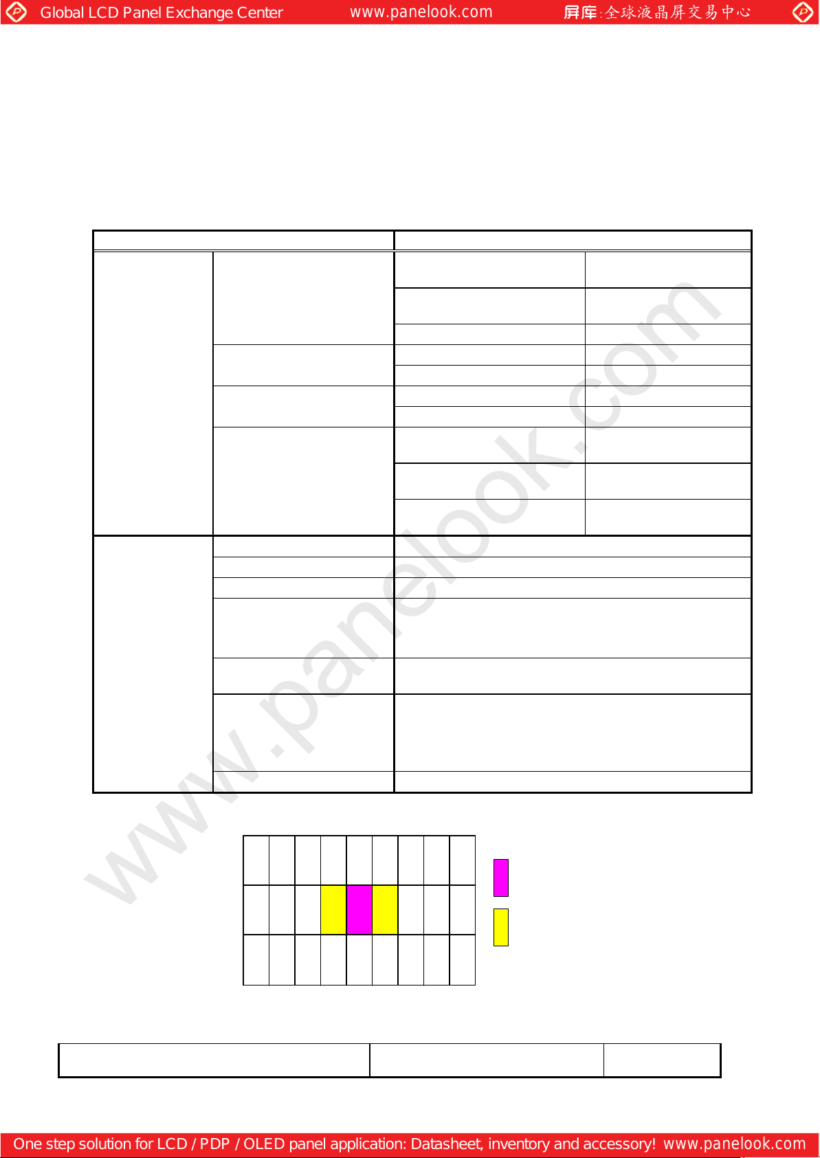
Bright Dot is defined as follows:
Visible through 5% transmission ND filter under the condition that black image (color 0) is on the
display.
DEFECT TYPE LIMIT
SCRATCH
DENT
VISUAL
DEFECT
ELECTRICAL
DEFECT
*1) W: width,L: length,φ : diameter,N: number
*2) DEFINITION OF ADJACENT
BLACK SPOT
BUBBLE
BRIGHT DOT N ≤ 5
DARK DOT N ≤ 5
TOTAL DOT N ≤ 8
TWO ADJACENT DOT
BRIGHT DOT ≤ 2 PAIRS
DARK DOT ≤ 2 PAIRS
THREE OR MORE
ADJACENT DOT
DISTANCE BETWEEN
DEFECTS
BRIGHT DOT ≥ 15 mm
DARK DOT ≥ 15 mm
LINE DEFECT NOT ALLOWED
LINT
0.01 mm < W ≤ 0.05 mm
L ≤ 10 mm
0.01 mm < W
10 mm < L
0.05 mm < W N = 0
0.2 mm < φ ≤ 0.4 mm N ≤ 4
0.4 mm < φ N = 0
0.2 mm < φ ≤ 0.4 mm N ≤ 5
0.4 mm < φ N = 0
L ≤ 3 mm
W ≤ 0.1 mm
3 mm < L
W ≤ 0.1 mm
0.1 mm < W
N ≤ 4
N = 0
N ≤ 4
N = 0
ACCORDING TO
BLACK SPOT
NOT ALLOWED
GR BR G B R G B
Defective Dot
GR BR G B R G B
Adjacent Dots
GR BR G B R G B
The defects that are not defined above and considered to be problem shall be reviewed and discussed by
both parties.
T-51784D150-FW-A-AA (AA) No. 2003-0143 OPTREX CORPORATION Page 19/35
Page 20

Global LCD Panel Exchange Center
www.panelook.com
One step solution for LCD / PDP / OLED panel application: Datasheet, inventory and accessory!
www.panelook.com
11. HANDLING PRECAUTIONS FOR TFT-LCD MODULE
Please pay attention to the followings in handling TFT-LCD products;
(1) ASSEMBLY PRECAUTION
a. Please mount the LCD module by using mounting hole with a screw clamping torque less than 0.5
Nm. Please do not bend or wrench the LCD module in assembling. Please do not drop, bend or twist
the LCD module in handling. Please mount the invertor circuit board by using mounting hole of
rear side with a screw clamping torque less than 0.2 Nm.
b. Please design display housing in accordance with the following guide lines.
(a) Housing case must be designed carefully so as not to put stresses on LCD all sides and not to
wrench module. The stresses may cause non-uniformity even if there is no non-uniformity
statically.
(b) Keep sufficient clearance between LCD module back surface and housing when the LCD
module is mounted. Approximately 1.0mm of the clearance in the design is recommended taking
into account the tolerance of LCD module thickness and mounting structure height on the
housing.
(c) When some parts, such as, FPC cable and ferrite plate, are installed underneath the LCD
module, still sufficient clearance is required, such as 0.5mm. This clearance is, especially, to be
reconsidered when the additional parts are implemented for EMI countermeasure.
(d) Design the inverter location and connector position carefully so as not to give stress to lamp
cable, or not to interface the LCD module by the lamp cable.
(e) Keep sufficient clearance between LCD module and the others parts, such as inverter and
speaker so as not to interface the LCD module. Approximately 1.0mm of the clearance in the
design is recommended.
c. Please do not push or scratch LCD panel surface with anything hard. And do not soil LCD panel
surface by touching with bare hands. (Polarizer film, surface of LCD panel is easy to be flawed.)
d. Please do not press any parts on the rear side such as source TCP, gate TCP, control circuit board
and FPCs during handling LCD module. If pressing rear part is unavoidable, handle the LCD
module with care not to damage them.
e. Please wipe off LCD panel surface with absorbent cotton or soft cloth in case of it being soiled.
f. Please wipe off drops of adhesives like saliva and water on LCD panel surface immediately. They
might damage to cause panel surface variation and color change.
g. Please do not take a LCD module to pieces and reconstruct it. Resolving and reconstructing modules
may cause them not to work well.
h. Please do not touch metal frames with bare hands and soiled gloves. A color change of the metal
frames can happen during a long preservation of soiled LCD modules.
T-51784D150-FW-A-AA (AA) No. 2003-0143 OPTREX CORPORATION Page 20/35
Page 21

Global LCD Panel Exchange Center
www.panelook.com
One step solution for LCD / PDP / OLED panel application: Datasheet, inventory and accessory!
www.panelook.com
i. Please pay attention to handling lead wire of backlight so that it is not tugged in connecting with
inverter.
j. Please connect the metal frame of LCD module to GND in order to minimize the effect of external
noise and EMI.
k. Be sure to connect the cables and the connectors correctly.
(2) OPERATING PRECAUTIONS
a. Please be sure to turn off the power supply before connecting and disconnecting signal input cable.
b. Please do not change variable resistance settings in LCD module. They are adjusted to the most
suitable value. If they are changed, it might happen LCD does not satisfy the characteristics
specification.
c. LCD backlight takes longer time to become stable of radiation characteristics in low temperature
than in room temperature.
d. The interface signal speed is very high. Please pay attention to transmission line design and other
high speed signal precautions to satisfy signal specification.
e. A condensation might happen on the surface and inside of LCD module in case of sudden change of
ambient temperature.
f. Please pay attention not to display the same pattern for very long time. Image might stick on LCD.
Even if image sticking happens, it may disappear as the operation time proceeds.
g. Please obey the same safe instructions as ones being prepared for ordinary electronic products
(3) PRECAUTIONS WITH ELECTROSTATICS
a. This LCD module use CMOS-IC on circuit board and TFT-LCD panel, and so it is easy to be affected
by electrostatics. Please be careful with electrostatics by the way of your body connecting to the
ground and so on.
b. Please remove protection film very slowly from the surface of LCD module to prevent from
electrostatics occurrence.
(4) STORAGE PRECAUTIONS
a. Please do not leave the LCDs in the environment of high humidity and high temperature such as
60°C90% RH.
b. Please do not leave the LCDs in the environment of low temperature; below -20°C.
(5) SAFETY PRECAUTIONS
T-51784D150-FW-A-AA (AA) No. 2003-0143 OPTREX CORPORATION Page 21/35
Page 22

Global LCD Panel Exchange Center
www.panelook.com
One step solution for LCD / PDP / OLED panel application: Datasheet, inventory and accessory!
www.panelook.com
a. When you waste damaged or unnecessary LCDs, it is recommended to crush LCDs into pieces and
wash them off with solvents such as acetone and ethanol, which should later be burned.
b. If any liquid leaks out of a damaged glass cell and comes in contact with the hands, wash off
thoroughly with soap and water.
c. Be sure to turn off the power supply when inserting or disconnecting the cable.
d. Inverter should be designed carefully so as not to keep working in case of detecting over current or
open circuit on the lamp.
(6) OTHERS
a. A strong incident light into LCD panel might cause display characteristics changing inferior
because of polarizer film, color filter, and other materials becoming inferior. Please do not expose
LCD module direct sunlight and strong UV rays.
b. Please pay attention to a panel side of LCD module not to contact with other materials in
preserving it alone.
c. For the packaging box, please pay attention to the followings;
(a) Packaging box and inner case for LCD are designed to protect the LCDs from the damage or
scratching during transportation. Please do not open except picking LCDs up from the box.
(b) Please do not pile them up more than 5 boxes. (They are not designed so.) And please do not
turn over.
(c) Please handle packaging box with care not to give them sudden shock and vibrations. And also
please do not throw them up.
(d) Packaging box and inner case for LCDs are made of cardboard. So please pay attention not to
get them wet. (Such like keeping them in high humidity or wet place can occur getting them
wet.)
T-51784D150-FW-A-AA (AA) No. 2003-0143 OPTREX CORPORATION Page 22/35
Page 23
Global LCD Panel Exchange Center
www.panelook.com
One step solution for LCD / PDP / OLED panel application: Datasheet, inventory and accessory!
www.panelook.com
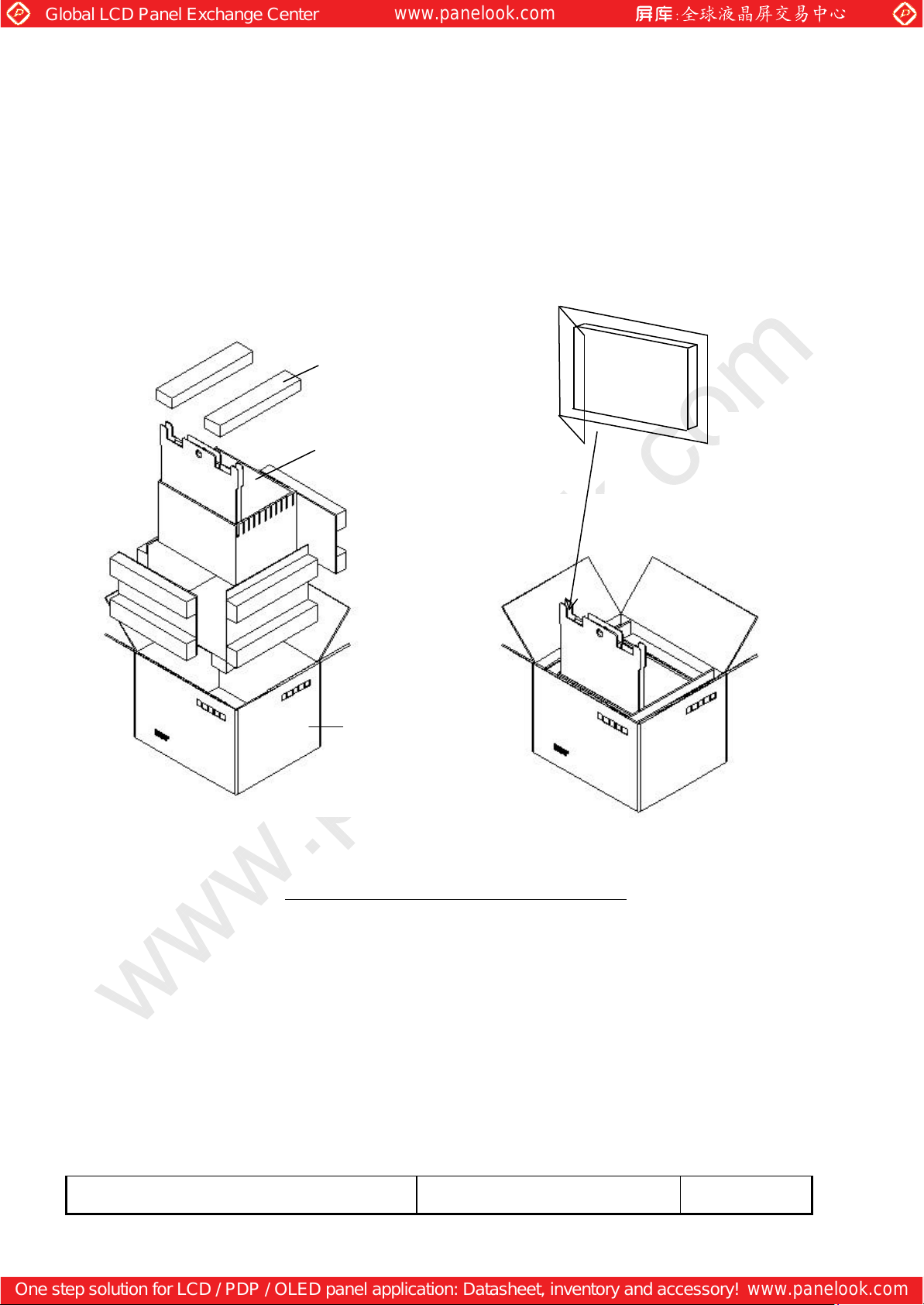
Packaging specification
1. Packaging box
material: cardboard
construction: See fig. 1
max. packaging number: 10 pcs.
dimension: 488 (W) × 395 (H) × 361 (D)[mm]
mass(including 10 modules): 17.8 kg
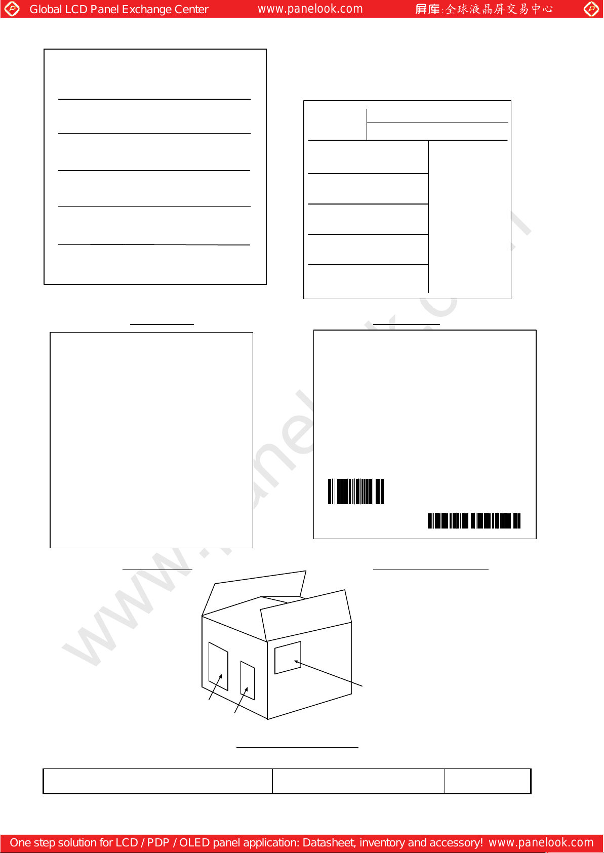
label: Labels are put on the box.(See fig. 2, 3, 4)
T op cover
LCD
Inner box
Outside box
Fig. 1. Illustration of packaging box structure
T-51784D150-FW-A-AA (AA) No. 2003-0143 OPTREX CORPORATION Page 23/35
Page 24
Global LCD Panel Exchange Center
www.panelook.com
One step solution for LCD / PDP / OLED panel application: Datasheet, inventory and accessory!
www.panelook.com
収納
バーコー
シリアル番
バーコー
バーコー
バーコー
シリアル番
シリアル番
シリアル番
バーコー
シリアル番
バーコー
バーコー
バーコー
シリアル番
シリアル番
シリアル番
Bar-code
Serial No.
Bar-code
Serial No.
Bar-code
Bar-code
Serial No.
Bar-code
Serial No.
Bar-code
Serial No.
Bar-code
Serial No.
Bar-code
Serial No.
Bar-code
Serial No.
Bar-code
Serial No.
Bar-code
Serial No.
Bar-code
Bar-code
Bar-code
型
Product name
Packaging number
バーコー
シリアル番
バーコー
Fig.2. Label1 Fig.3. Label 2
Consignee
Product name
Product name of consignee
Order No.
バーコー
シリアル番
バーコー
Shipper
Box No.
Mass
Shipping No.
Bar-code
Shipping No.
Bar-code
Packaging No.
Shipping No.
Products name
Bar-code
OPTREX
TFT - LCD: AA150XK01
T-51784D150-FW-A-AA
P / O NO. 123456789
Box No.
Place of production
Bar-code
Shipping date
Fig. 4. Label 3 Fig. 5 Sample of Label3
Fig. 4. Label 3 Fig. 5 Sample of Label3
Label 1
C / S 001 OF 005
MADE IN JAPAN
001 JA1BK4144
2001/11/15
Label 3
Label 2
Fig. 6. Location of Labels
T-51784D150-FW-A-AA (AA) No. 2003-0143 OPTREX CORPORATION Page 24/35
Page 25
Global LCD Panel Exchange Center
www.panelook.com
One step solution for LCD / PDP / OLED panel application: Datasheet, inventory and accessory!
www.panelook.com
2. Location of label on the packaging box
l Labels are put on the box.(See Fig.6)
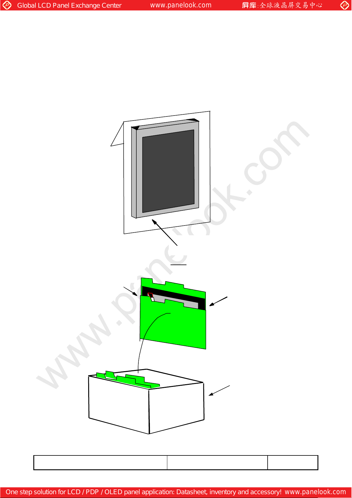
3. Packaging form of product
l Each of LCD module is packed in anti-electrostatic bag(Fig. 7)
l Packed LCD module is put in the packaging box.(Fig. 8)
The packaging box accumulates maximum 10 modules.
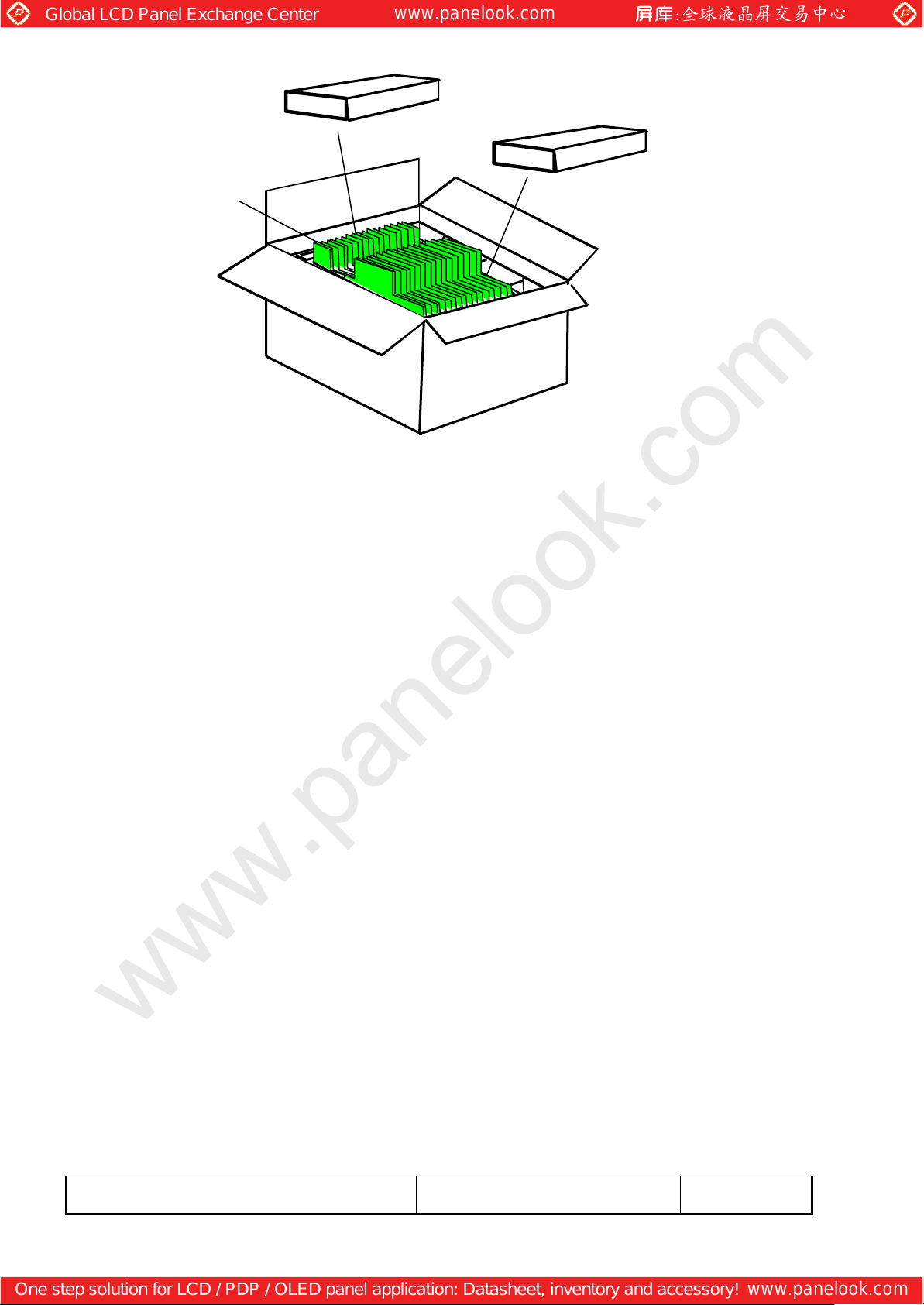
l Upper protector is put on the products and shut the box.(Fig. 9)
Product in
Anti-elctrostatic bag
(Surface)
Fig. 7
Lamp lead Product in
Anti-elctrostatic bag
Inner box
Fig. 8
T-51784D150-FW-A-AA (AA) No. 2003-0143 OPTREX CORPORATION Page 25/35
Page 26
Global LCD Panel Exchange Center
www.panelook.com
One step solution for LCD / PDP / OLED panel application: Datasheet, inventory and accessory!
www.panelook.com
Inner box
Top cover
Fig. 9
4. Cautions of shipping & storage
l Do not turn the packaging upside down while storage and transportation. The boxes should not be
piled up more than 5.
l Handle with care. Keep off from rain & dew.
l Keep off from direct sunlight exposure. Please store under room temperature & low humidity in
original packaging condition when they were shipped.
l Keep other cautions described in handling manual.
T-51784D150-FW-A-AA (AA) No. 2003-0143 OPTREX CORPORATION Page 26/35
Page 27
Global LCD Panel Exchange Center
www.panelook.com
One step solution for LCD / PDP / OLED panel application: Datasheet, inventory and accessory!
www.panelook.com
E158720
Products Number Labeling Forms
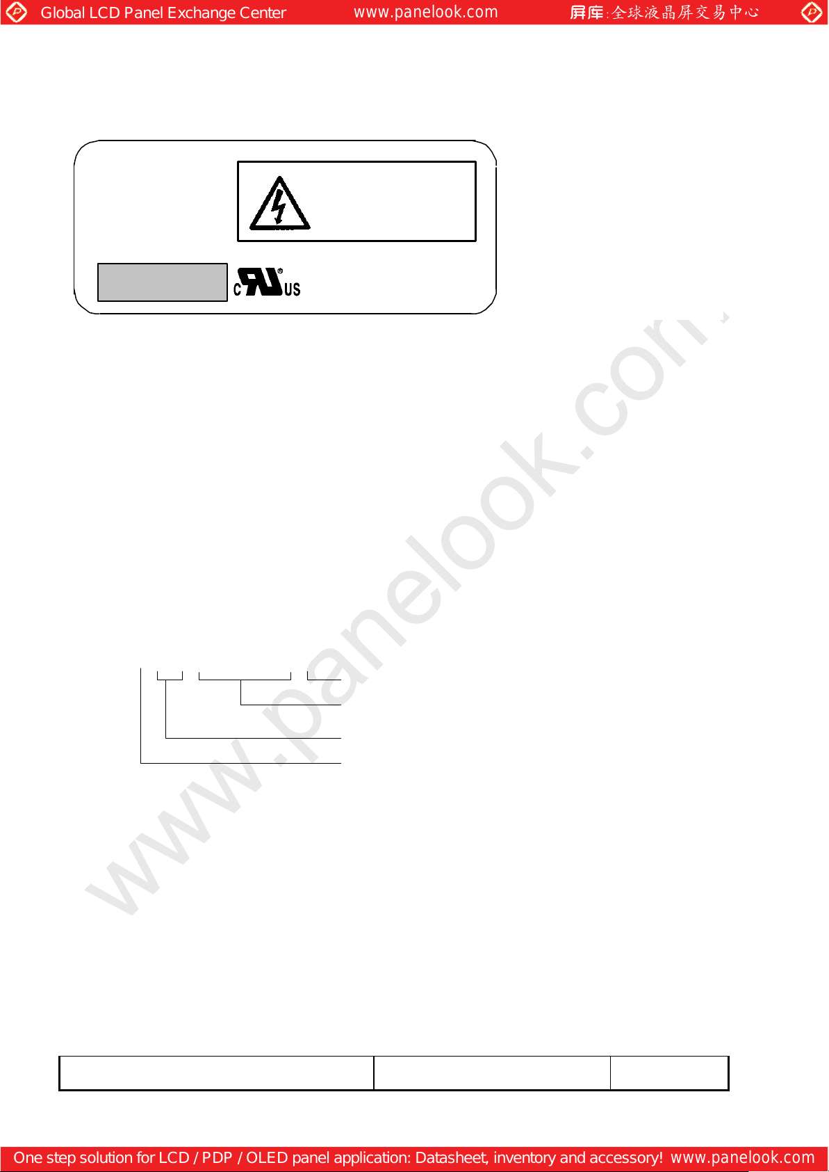
Products number label is constructed as below;
①
Brand Name, Symbol
②
T-51512D121-FW-A-AA
③
AA121SK26
④
ABC1234567890
⑤
60100001L
⑥
Bar-code
① Brand Name, Symbol
OPTREX
② Products Name of Optrex
⑦ ⑧
WARNING
LAMP HIGH
VOLTAGE
Made in Japan
①
Brand Name, Symbol
②Products Name of Optrex
③Products Name
④
Production Key Number(13Digits)
⑤
Date Code
(Serial Number, Factory Sign )
⑥Bar-code of Date Code
⑦
UL File No.
⑧Production Country
ex. T51512D121-FW-A-AA
③ Products Name
ex.1: AA121SK26 ex.2: AA150XA03 B
④ Production Key Number(13Digits)
(ID Number for Production Control)
⑤Date Code(Serial Number, Factory Sign)
□□□□□□□□□
123456789
Factory Sign
Serial Number on Every Production Week
(00001 〜 99999)
Production Week Number(01 〜53)
Production Year Number
(Last 1 Digit of AD Year Number)
・Date Code is constructed by 9 Digits as below;
1st Digit :Production Year Number(Last 1 Figure of AD Year)
2nd〜3rd Digit : Production Week Number in a Year
(A Year is divided to 53 weeks from Monday to Saturday)
4th〜8th Digit :Serial Number on Every Production Weeks.
( 00001 〜 99999 )
These are numbered in order according to Production Name.
9th Digit :Factory Sign ( on the Module Test Process)
( L: Shisui Factory Line, Y: YACHIYO SANYO Industries Line,
W: CPT Fab-1, R: CPT Fab-2 , U: CPT Wujiang-LCM)
T-51784D150-FW-A-AA (AA) No. 2003-0143 OPTREX CORPORATION Page 27/35
Page 28

Global LCD Panel Exchange Center
www.panelook.com
One step solution for LCD / PDP / OLED panel application: Datasheet, inventory and accessory!
www.panelook.com
⑥Bar-code(Date Code)
Bar-code Line for computer reading Date Code mentioned as above.
⑦UL File No.
ADI: E158720, CPT: E194548
⑧Production Country
ADI: Made in Japan, CPT: Made in Taiwan
T-51784D150-FW-A-AA (AA) No. 2003-0143 OPTREX CORPORATION Page 28/35
Page 29
Global LCD Panel Exchange Center
www.panelook.com
One step solution for LCD / PDP / OLED panel application: Datasheet, inventory and accessory!
www.panelook.com
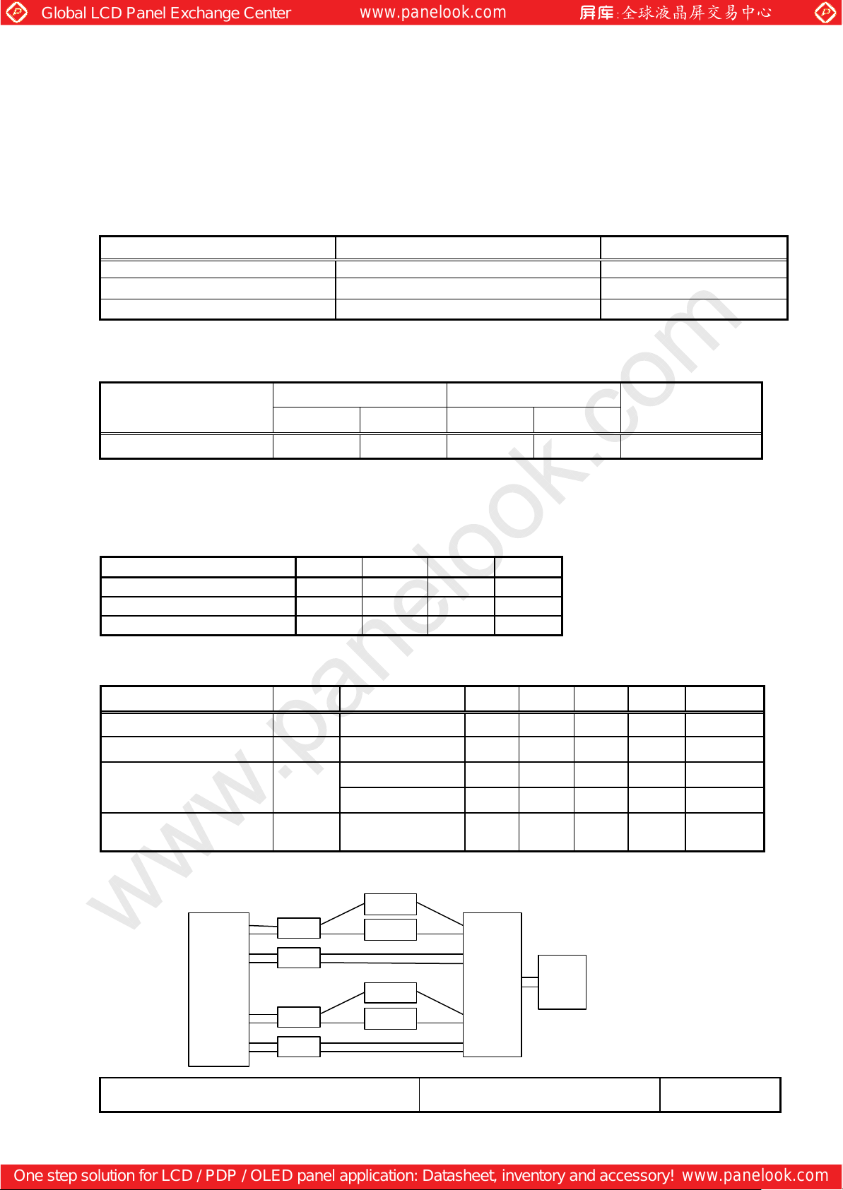
Outline Dimension of Reflector
324.0±0.6 × 7.0±0.1
Except wire
CTL
CTL
LAMP UNIT for 15.0"XGA
APPLICATION
This technical literature applies to the replaceable lamp unit that is the maintenance parts for
15.0”XGA TFT-LCD module industrial use(model name:T-51784D150-FW-A-AA).
(AA-L5902147(Top), AA-L5902148(Bottom))
MECHANICAL CHARACTERISTICS
Item Specification Remarks
Mass 22±3(g)(MAX) With wire and connector
Lamp Diameter φ 2.4-1.8 (mm)
See DRAWING OF OUTLINE DIMENTIONS
ENVIRONMENTAL CONDITIONS
Item
Operation Non Operation
Remarks
MIN MAX MIN MAX
Ambient Temperature 0°C 50°C -25°C 60°C No Condensation
Top,Tstg ≤ 40°C : 90%RH max. without condensation
Top,Tstg > 40°C : Absolute humidity shall be less than the value of 90%RH at 40°C without
condensation.
ABSOLUTE MAXIMUM RATINGS
Item Symbol MIN MAX UNIT
Lamp Current IL 0 9.0 mArms
Lamp Voltage VL 0 2500 Vrms
Lamp Frequency FL 0 100 kHz
ELECTRICAL CHARACTERISTICS
Item Symbol Condition MIN TYP MAX Unit Remarks
Lamp Current IL Ta = 25°C 3.5 6.5 8.0
Lamp Voltage VL Ta = 25°C - 595 - Vrms
Ta = 25°C 1000 - - Vrms
Starting Lamp Voltage VS
Ta = 0°C 1350 - - Vrms
Lamp Frequency FL
Ta = 25℃,
IL = 6.5 mArms
40 - 70 kHz
*1) These values are shown by ALPUS Electric using ALPS-UHP061095 inverter.
*2) Lamp Current measurement method (The current meter is inserted in low voltage line.)
mArm
CTL
CTH
LCD
Module
T-51784D150-FW-A-AA (AA) No. 2003-0143 OPTREX CORPORATION Page 29/35
CTH
CTL
CTH
CTH
A
A
A
A
Inverter
Power
Supply
Page 30
Global LCD Panel Exchange Center
www.panelook.com
One step solution for LCD / PDP / OLED panel application: Datasheet, inventory and accessory!
www.panelook.com
768
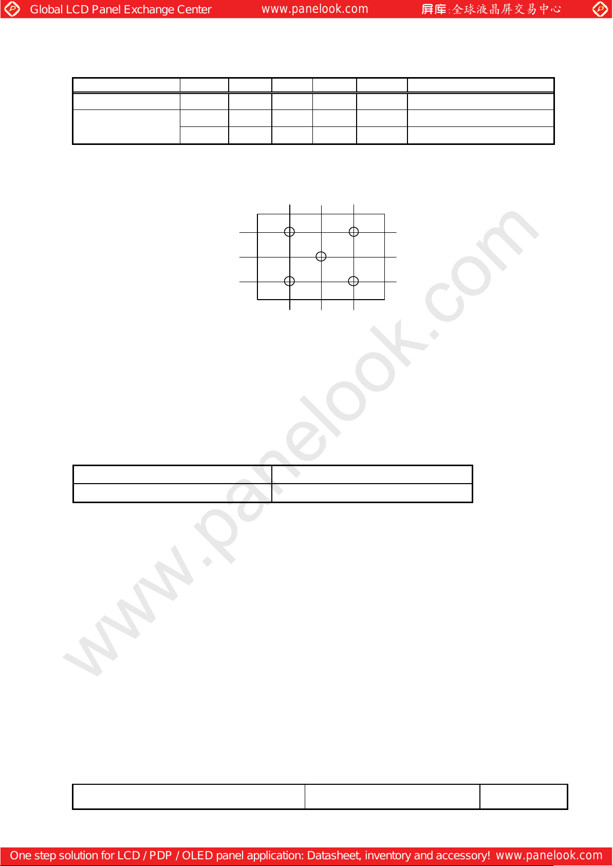
OPTICAL CHARACTERISTICS
Item Symbol MIN TYP MAX Unit Remarks
Luminance Lw 360 450 -- cd/m
Color Coordinates
(White)
[Conditions]
IL=6.5 mArms, Inverter frequency: 60kHz
[Measurement Point]
Wx
Wy
0.253 0.283 0.313
0.267 0.297 0.327
Ta=25°C, 60±10%RH
2
Average of below 5 points
- Value of center point(5)
- Value of center point(5)
(1,1)
192
384
576
256 512
1
3
2
5
4
(1024,768)
These items are measured when lamp units are assembled into T-51784D150-FW-A-AA, and
using CS1000(MINOLTA) for color coordinates, and CS1000 or BM-5A(TOPCON) for others
under the dark room condition (no ambient light) after more than 30 minutes from turning on
the lamp unless noted.
LIFE TIME OF THE LAMP UNIT
Environmental Conditions are as follows:
Ambient temperature is 25±5°C.
Lamp Current is 6.5 mArms.
Continuous Operation 50,000 h
Number of turning on and off 100,000 times (30 sec ON-OFF)
(1) Lamp life time is defined as the time either when the brightness becomes 50% of the initial
value, or when the starting lamp voltage does not meet the value specified in the table of
section 4.
(2) The life time of the backlight depends on the ambient temperature. The life time will decrease
under low/high temperature.
(3) Following standards should be satisfied
・No flickers should be allowed.
・Decrease in luminous length that is caused by lamp blacking is within 11 mm from the
edge of the lamp.
T-51784D150-FW-A-AA (AA) No. 2003-0143 OPTREX CORPORATION Page 30/35
Page 31
Global LCD Panel Exchange Center
www.panelook.com
One step solution for LCD / PDP / OLED panel application: Datasheet, inventory and accessory!
www.panelook.com
INTERFACE PIN CONNECTION
(1) CN 3, 4(Backlight)
Backlight-side connector: BHSR-02VS-1(JST)
Inverter-side connector: SM02B-BHSS-1-TB
Pin No. Symbol Function
1, 2 CTH VBLH(High Voltage)
[Note] VBLH-VBLL = VL
(2) CN 5, 6(Backlight)
Backlight-side connector: BHR-02VS-1(JST)
Inverter-side connector: SM02(4.0)B-BHS-1-TB
Pin No. Symbol Function
1, 2 CTL VBLL(Low Voltage)
[Note] VBLH-VBLL = VL
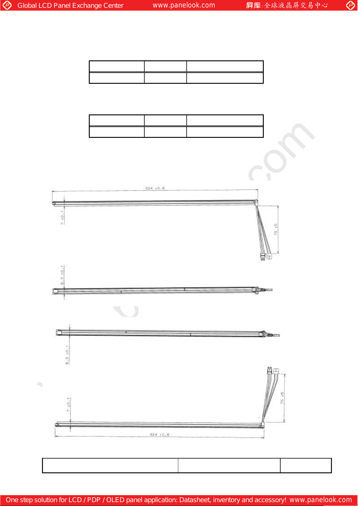
DRAWING OF OUTLINE DIMENTIONS
(1) AA-L5902147(Top)
(2) AA-L5902148(Bottom)
T-51784D150-FW-A-AA (AA) No. 2003-0143 OPTREX CORPORATION Page 31/35
Page 32
Global LCD Panel Exchange Center
www.panelook.com
One step solution for LCD / PDP / OLED panel application: Datasheet, inventory and accessory!
www.panelook.com
matters.
METHOD OF REPLACING THE LAMP UNIT
(1) Precautions
Please pay attention to the following items while replacing the Lamp Unit.
a. Please do not damage the LCD Panel Surface, and do not touch it with bare hands.
(Wearing gloves is recommended.)
b. Please be careful with electrostatics, and work in clean environment to prevent entering dust
and/or foreign matters that will cause bad display image.
(Using clean bench or similar environment is recommended.)
c. Please be careful of the edge of the frame metal.
d. Please replace top and bottom lamp units at the same time. Replace only one lamp unit
will cause inferior display image.
(2) Method of replacing the Lamp Unit
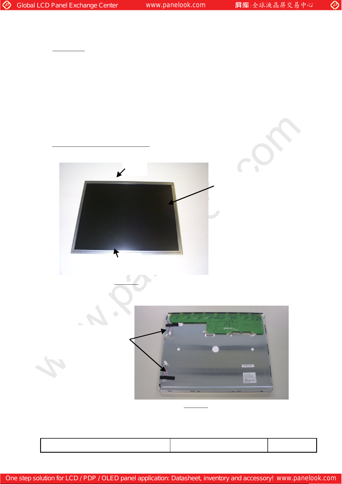
1) Put the TFT-LCD Module on the table.(LCD Panel Surface is upside.)
Top
Bottom
Picture 1
2) Turn the TFT-LCD Module upside down.
Please check the rear
surface for dust and foreign
Please check the LCD Panel
Surface for scratch, dust, and
foreign matters.
Picture 2
T-51784D150-FW-A-AA (AA) No. 2003-0143 OPTREX CORPORATION Page 32/35
Page 33
Global LCD Panel Exchange Center
www.panelook.com
One step solution for LCD / PDP / OLED panel application: Datasheet, inventory and accessory!
www.panelook.com
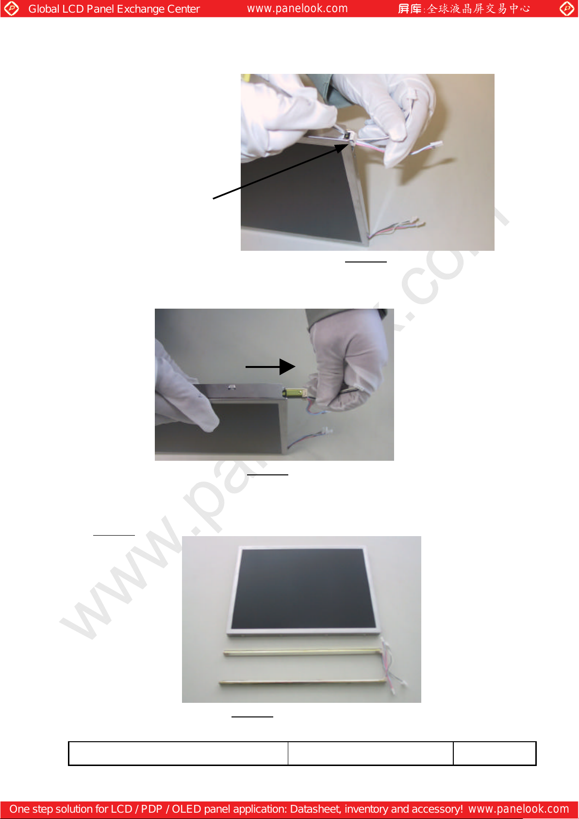
3) Stand the TFT-LCD Module up and push down the latch of rubber holder with that Lamp
Unit fastens using a screw driver(-) and the like.
Push down the latch of rubber
holder.
4) Pull the black cable and white one slowly and remove the Lamp Unit.(Do not tug at the pink
cable and blue one.)
Picture 3
Picture 4
5) Remove the other Lamp Unit at the opposite(bottom) side of LCD Module in the same way.
See.3) and 4)
6) Picture 5 shows the TFT-LCD Module after removing the Lamp Units.
Picture 5
T-51784D150-FW-A-AA (AA) No. 2003-0143 OPTREX CORPORATION Page 33/35
Page 34
Global LCD Panel Exchange Center
www.panelook.com
One step solution for LCD / PDP / OLED panel application: Datasheet, inventory and accessory!
www.panelook.com
7) Prepare to insert the new Lamp Units.
• Open the package and take the new Lamp Units out.
• Check the new Lamp Units for dust and foreign matters.
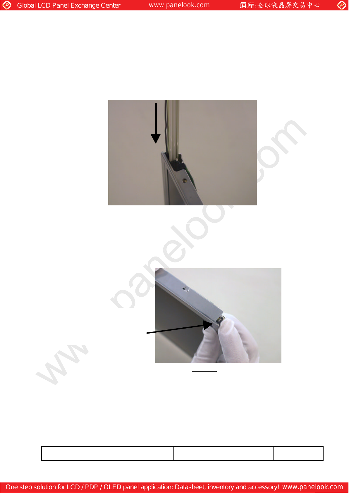
8) Stand the TFT-LCD module up and insert the new Lamp Unit.
The light guide and reflector sheet should be inside of the Lamp Unit.
Please be careful not to hurt your hands from the edge of the Lamp Unit.
Please pay attention to insert direction.
Picture 6
9) Please insert Lamp Unit. After inserting the Lamp Unit, please check that the Lamp Unit is
fastened with the latch of rubber holder.
Please be careful not to tug at and bend the wire hard in handling.
Please check that the Lamp Unit is
fastened with the latch of rubber
holder.
Picture 7
T-51784D150-FW-A-AA (AA) No. 2003-0143 OPTREX CORPORATION Page 34/35
Page 35
Global LCD Panel Exchange Center
www.panelook.com
One step solution for LCD / PDP / OLED panel application: Datasheet, inventory and accessory!
www.panelook.com
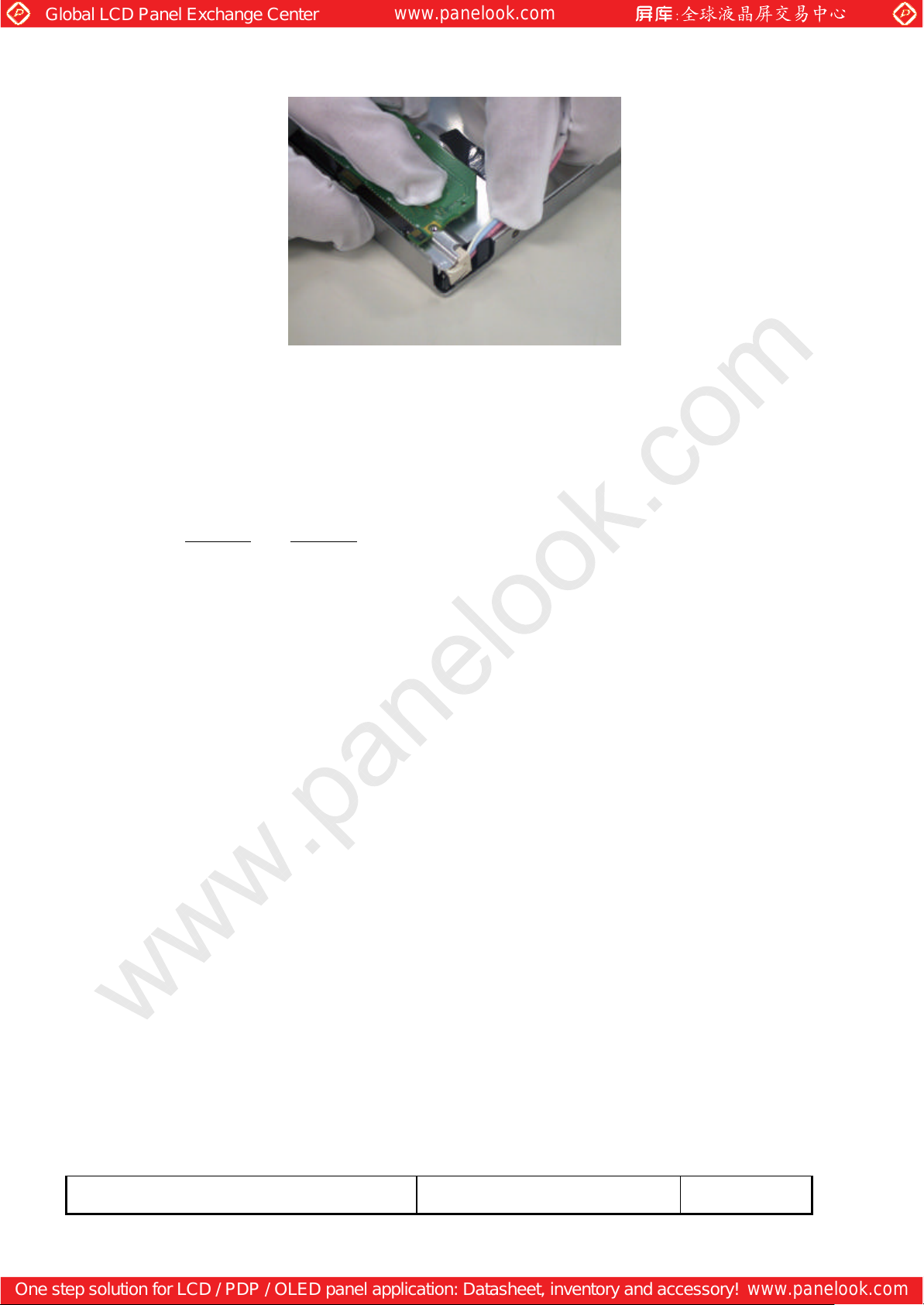
10) Put the lamp cables in the trench of the plastic frame to keep inside of the module.
11) Insert the other Lamp Unit to the opposite(bottom) side of the LCD module in the same way.
See. 8) to 10)
12) After replacing the Lamp Units, please check the following items.
• Appearance of TFT-LCD Module is not changed after replacing Lamp Units.
(See. Picture 1 and Picture 2)
• There is no damage, dust, or foreign matters on the LCD Panel Surface.
• Install the TFT-LCD Module then check turning on the lamps.
Picture 8
T-51784D150-FW-A-AA (AA) No. 2003-0143 OPTREX CORPORATION Page 35/35
 Loading...