

OPTREX T-51446L050J-FW-P-AB Datasheet
Rev.
Date
Page
Comment
First Edition
Mar 27, 2002
Final Revision
******
OP T R E X
LCD Module Technical Specification
T-51446L050J-FW-P-AB
Tentative
Table of Contents
1. Applications
2. Features
3. Mechanical Specifications
4. Mechanical Drawing TFT LCD Module
5. Input / Output Terminals
6. Absolute Maximum Ratings
7. Electrical Characteristics
8. Power Sequence
9. Optical Characteristics
10. Handling cautions
11. Reliability TEST
12. Labeling
13. Block Diagram
Revision History
........................................................................................................................................
.......................................................................................................................................
Checked by (Quality Assurance Div.)
Checked by (Design Engineering Div.)
Prepared by (Production Div.)
.................................................................................................................................
................................................................................................
..................................................................
..................................................................................................
..............................................................................................
.....................................................................................................
..................................................................................................................
......................................................................................................
................................................................................................................
.....................................................................................................................
.........................................................................................................................
2
2
2
3
4
6
6
15
16
19
20
20
21
T-51446L050J-FW-P-AB
OPTREX CORPORATION
Page 1/21

1. Application
This technical specification applies to 5” color TFT-LCD module. The applications of the
panel are car TV , portable DVD and GPS.
2. Features
. Compatible with NTSC & PAL system
. Pixel in stripe configuration
. Slim and compact
. Vcom Toggle
. Image Reversion : Up/Down and Left/Right
3. Mechanical Specifications
Parameter Specifications Unit
Screen Size 5 (diagonal) inch
Display Format
Active Area
Dot Pitch
Pixel Configuration Stripe
Outline Dimension
Weight 160±10 g
102.72 (H)×74.53 (V)
127.4 (W)×92.8 (H)×12.9 (D)(typ.)
960×234
0.107 (H)×0.319 (V)
dot
mm
mm
mm
T-51446L050J-FW-P-AB
OPTREX CORPORATION
Page 2/21
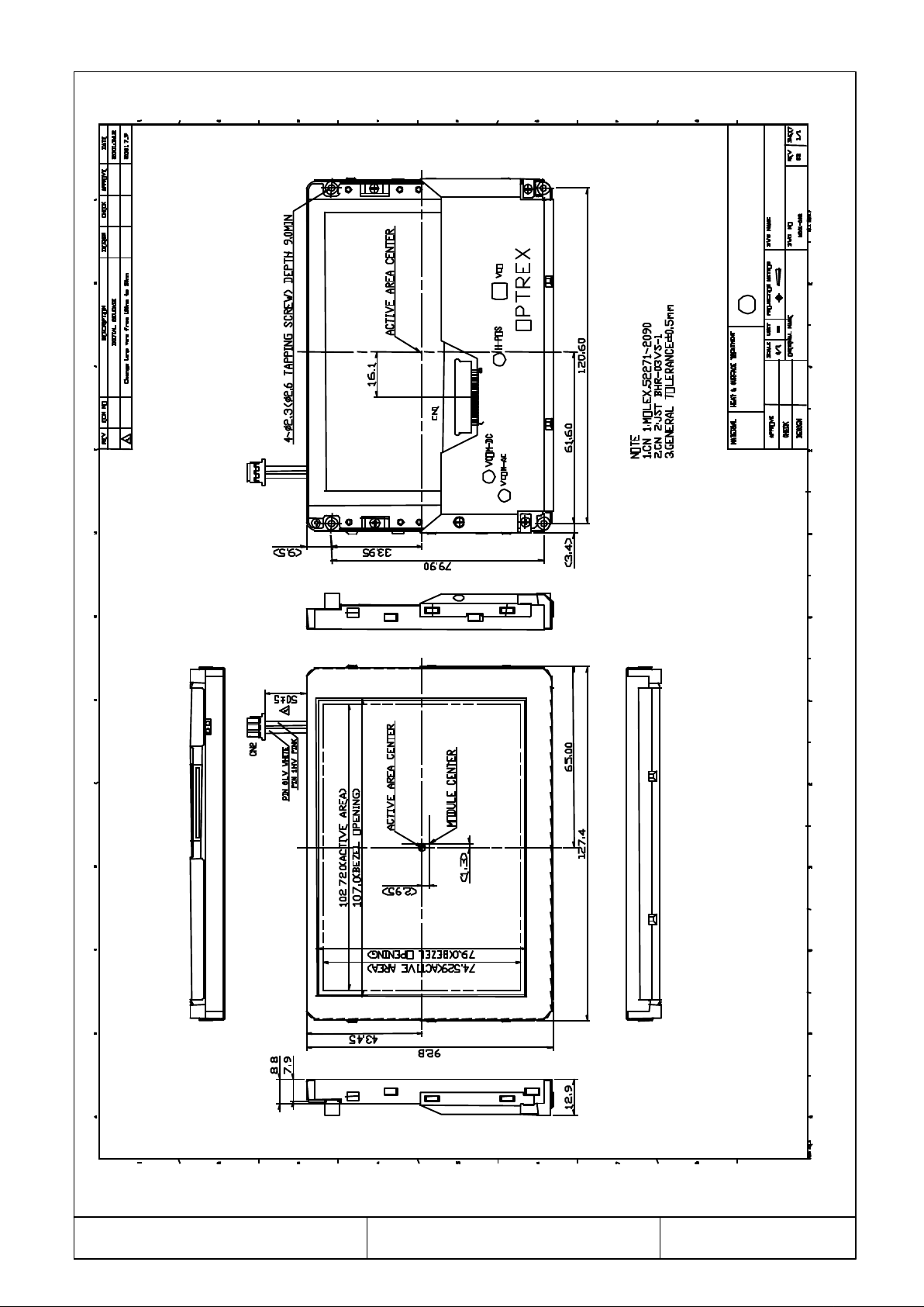
4. Mechanical Drawing of TFT-LCD Module
T-51446L050J-FW-P-AB
OPTREX CORPORATION
Page 3/21
5. Input / Output Terminals
5-1) TFT-LCD Panel Driving
Pin No Symbol I/O Description Remark
1 HSY I/O Horizontal Sync. Input / Output
2 FRP O Video Polarity Alternating Signal
3 CSY/HSY I Composite Sync. Signal Note 5-1
4 V
5 V
6 V
7 V
8 V
GH
GL
B
R
G
I Supply Voltage for Gate Driver (Hi level) Note 5-2
I Supply Voltage for Gate Driver (Low level) Note 5-3
I Video Signal (Blue)
I Video Signal (Red)
I Video Signal (Green)
9 GND I Ground
10 V
11 V
DD
CC
I Supply voltage for Controller Note 5-4
I Supply voltage for source driver Note 5-5
12 GND I Ground
13 CKC I Control pin for select I/O signal Note 5-1
14
VSY
I/O Vertical Sync. Input/ Output
15 PSI O Synchronize Pulse for Decoder
16 PSC O Synchronize Pulse for DC-DC Converter
17 NC I No Connection /Vertical sync. Signal Note 5-1
18 UD I UP/DOWN Control Note 5-7
19 RL I Right/Left Shift Control Note 5-6
20 NP I/O NTSC/PAL Selection Signal(Low : PAL, High : NTSC) Note 5-8
Note 5-1-1 : PVI’S module can support 2 input mode .
CKC of 26 pin select 2 input mode.
Parameter Select pin(CKC) Description
CKC CSY/HD NC/VD
Composite sync mode High CSY (positive edge) -
Sync separate mode Low HD(negative edge) VD(positive edge)
Note 5-1-2The default mode of PVI module is composite sync mode (CKC= high)
Note 5-1-3: If you use sync separate mode (CKC= low),please contact PVI.
Note 5-2:VGHTYP.=+17V
Note 5-3:VGLTYP.=-15V
T-51446L050J-FW-P-AB
OPTREX CORPORATION
Page 4/21
Note 5-4:VDDTYP.=+5V
Note 5-5:VCCTYP.=+5V
Note 5-6 : Low (0V) for shift Right; Input Hi (+5.0V) for inverse (shift Left).
Note 5-7 : Hi (+5.0V) for DOWN; Low (0V) for UP.
Note 5-8 : PAL= LOW(0V),NTSC= Hi(+5.0V) :
( If use auto detect , this pin is output ,otherwise this pin is input.)
Low High
Note5-6 Right Left
Note5-7 Down Up
Note5-8 PAL NTSC
5-2) Backlight driving
Pin No Symbol Description Remark
1 VL1 Input terminal (Hi voltage side) Wire color : pink
3 VL2 Input terminal (Low voltage side)
Wire color : white
Note 5-9
Note 5-9 : Low voltage side of backlight inverter connects with Ground of inverter circuits.
5-3) Input / Output Connector
( MOLEX,52271-2090 )
A) LCD Module Connector
FFC Down Connector
20 Pins
Pitch : 1.0 mm
B) Backlight Connector
JST BHR-03VS-1
Pin No. : 3
Pitch : 4 mm
Pink : High Voltage
White : Low Voltage
T-51446L050J-FW-P-AB
OPTREX CORPORATION
Page 5/21
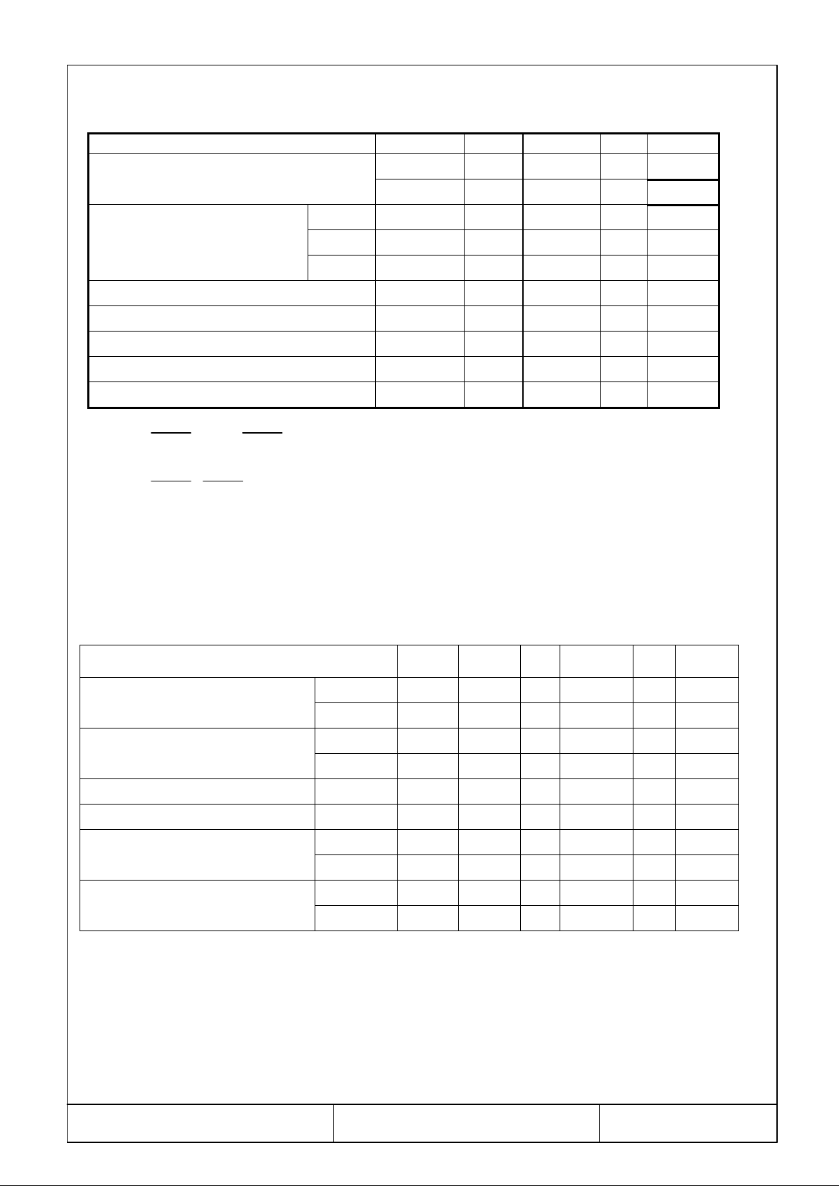
6. Absolute Maximum Ratings :
GND = 0 V,Ta = 25
Parameter Symbol MIN. MAX. Unit Remark
Supply Voltage For Source Driver
V
V
CC
DD
-0.5 7 V
-0.5 7 V
℃
Supply Voltage For Gate Driver
V
H Level V
L Level
VGL -20
GH-VGL
GH
-0.3 40 V
0 40 V
0 V
Analog Signal Input Level VR,VG,VB -0.3 7.0 V
Digital Input Signals -0.3 5.5 V Note 6-1
Digital Output Signals -0.3 5.5 V Note 6-2
Storage Temperature -30 +80
Operation Temperature -20 +70
℃
℃
Note 6-1 : HSY , CSY, VSY , CKC,
Note 6-2 : HSY , VSY , PSI, PSC
7. Electrical Characteristics
7-1) Recommended Operating Conditions:
A) Driving for TFT-LCD Panel
GND = 0V,Ta = 25
℃
Parameter Symbol MIN.
Analog V
CC
4.5 5.0 5.5 V
Typ MAX Unit Remark
Supply Voltage For Source Driver
Supply Voltage For Gate Driver
Logic V
H level V
L level V
DD
GH
GL
4.5 5.0 5.5 V
+15 +17 +19 V
-16 -15 -14 V
Supply Voltage For controller VDD 4.5 5.0 5.5 V
Analog Signal input Level
Amplitude 0.3 V
H level V
IH
0.7 V
DD
- V
0.3 V
CC-
DD
V
Digital input voltage
L level V
H level V
IL
OH
-0.3 - 0.3 V
0.7 V
DD
- V
DD
DD
V
V
Digital output voltage
L level V
OL
-0.3 - 0.3 V
DD
V
T-51446L050J-FW-P-AB
OPTREX CORPORATION
Page 6/21

B) Driving for backlight
GH
Ta= 25
℃
Parameter Symbol Min. Typ. Max. Unit Remark
Lamp voltage V
Lamp current I
Lamp frequency P
Kick-off voltage(25℃)
Kick-off voltage(0℃)
L
L
L
Vs --- --- 345 Vrms Note 7-2
Vs
387 430 473 Vrms IL= 5 mA
4.5 5.0 5.5 mA
40 43 80 KHz Note 7-1
--- --- 520 Vrms Note 7-2
Note 7-1 : The wave form of lamp driving voltage should be as closed to a perfect SIN wave as possible.
Note 7-2 : The Kick-off times≧1sec
7-2) Power Consumption
Ta=
℃
25
Parameter Symbol Conditions TYP. MAX Unit Remark
Supply current for Gate Driver (Hi level) I
Supply current for Gate Driver (Low level) I
Supply current for Source Driver I
Supply current for controller I
GH
GL
CC
DD
V
V
V
V
GL
CC
DD
=
=
=
=
+17V
-15V
+5V
+5V
0.15 0.20 mA
-10.0 -15.0 mA
17.0 20.0 mA
43.0 48.0 mA
LCD Panel Power Consumption 0.45 0.57 W Note 7-3
Backlight Lamp Power Consumption 2.65 2.80 W Note 7-4
Note 7-3 : The power consumption for backlight is not included.
Note 7-4 : Backlight lamp power consumption is calculated by I
7-3) Input / Output signal timing chart
FRP
Black
V
R
V
G
V
B
Black
CSY
White
×
VL.
L
4.5V
5V
0V
f=15.4kHz
Vcom
T-51446L050J-FW-P-AB
OPTREX CORPORATION
6.0V
Page 7/21
 Loading...