

OPTREX T-51410D104-FW-P-AF Datasheet
Rev.
Date
Page
Comment
OP T R E X
LCD Module Technical Specification
T-51410D104-FW-P-AF
First Edition
Dec 5, 2001
Final Revision
******
Checked by (Quality Assurance Div.)
***The part number and specification are still tentative.
Table of Contents
1. Applications................................................................................................................................................. 2
2. Features........................................................................................................................................................... 2
3. Mechanical Specifications................................................................................................................ 2
4. Mechanical Drawing TFT LCD Module ............................................................................ 3
5. Input / Output Terminals................................................................................................................. 4
6. Absolute Maximum Ratings.............................................................................................................6
7. Electrical Characteristics.....................................................................................................................6
8. Power Sequence.................................................................................................................................... 12
9. Optical Characteristics ..................................................................................................................... 13
10. Handling Cautions............................................................................................................................... 16
11. Reliability TEST.....................................................................................................................................17
12. Block Diagram.........................................................................................................................................18
Checked by (Design Engineering Div.)
Prepared by (Production Div.)
Revision History
T-51410D104-FW-P-AF
OPTREX CORPORATION
Page 1/18
1.Application
This data sheet applies to a color TFT LCD module, T-51410D104-FW-P-AF.
T-51410D104-FW-P-AF module applies to notebook PC, sub-note-book PC and other OA
product, which require high quality flat panel display.
This module is not designed for
aerospace, avionics, medical, F/A, transportation, car or any other products, which require
extreme level of reliability.
Optrex assumes no responsibility for any damage resulting from the use of the device which
dose not comply with the instructions and the precautions inthese specification sheet.
2. Features
. Amorphous silicon TFT LCD panel with back-light unit
. Pixel in stripe configuration
. Slim and compact, designed for O/A application
. Display Colors:262,144 colors
. Optimum Viewing Direction:12 o’clock
. 3.3V LVDS interface standard: DS90CF364 as receiver
. +3.3V DC supply voltage for TFT LCD panel driving
. Backlight driving DC/AC inverter not included in this module
. Wide Viewing Angle
3.Mechanical Specifications
Parameter Specifications Unit
Screen Size 26.4(diagonal) cm
10.4 (diagonal) inch
Display Format
Display Colors 262,144
Active Area
Pixel Pitch
Pixel Configuration Stripe
Outline Dimension
Weight 310(typ.),320(max.) g
Back-light Single CCFL, side-light type
Surface treatment Anti-glare and hard-coating
Display mode Normally white
800×(R, G, B)×600
211.2(H)×158.4 (V)
0.264 (H)×0.264 (V)
238.6 (w)×171.0(H)×6.0(typ.) (D)
dot
mm
mm
mm
T-51410D104-FW-P-AF
OPTREX CORPORATION
Page 2/18
4.Mechanical Drawing of TFT-LCD Module
Unit: mm
T-51410D104-FW-P-AF
OPTREX CORPORATION
Page 3/18
5.Input Terminals
5-1) TFT-LCD Panel Driving
Connector type: Molex55177-1491
Pin No. Symbol Function Remark
1 VDD Power supply : +3.3V
2 VDD Power supply : +3.3V
3 GND
4 GND
5 IN0- Pixel data Transmission pair 0 (negative -)
6 IN0+ Pixel data Transmission pair 0 (positive +)
7 IN1- Pixel data Transmission pair 1 (negative -)
8 IN1+ Pixel data Transmission pair 1 (positive +)
9 IN2- Pixel data Transmission pair 2 (negative -)
10 IN2+ Pixel data Transmission pair 2 (positive +)
11 CLK- Sampling Clock (negative -)
12 CLK+ Sampling Clock (positive +)
13 GND
14 GND
Recommended Transmitter (DS90C*363 of National Semiconductor) toT-51410D104-FW-
P-AF interface Assignment:
Input
terminal
of DS
Symbol No. Symbol Function
TIN0 44 R0 Red pixel data (LSB)
TIN1 45 R1 Red pixel data
TIN2 47 R2 Red pixel data Tout0- No.5 : IN0TIN3 48 R3 Red pixel data
TIN4 1 R4 Red pixel data Tout0+ No.6 : IN0+
TIN5 3 R5 Red pixel data(MSB)
TIN6 4 G0 Green pixel data (LSB)
TIN7 6 G1 Green pixel data
TIN8 7 G2 Green pixel data
TIN9 9 G3 Green pixel data Tout1- No.7 : IN1TIN10 10 G4 Green pixel data
TIN11 12 G5 Green pixel data(MSB) Tout1+ No.8 : IN1+
TIN12 13 B0 Blue pixel data(LSB)
TIN13 15 B1 Blue pixel data
TIN14 16 B2 Blue pixel data
TIN15 18 B3 Blue pixel data
TIN16 19 B4 Blue pixel data Tout2- No.9 : IN2TIN17 20 B5 Blue pixel data(MSB)
TIN18 22 NC No connection Tout2+ N0.10 : IN2+
TIN19 23 NC No connection
TIN20 25 ENAB Compound Synchronization
CLK in 26 NCLK Data sampling clock TCLK out-
90C*363
Graphic controller output signal Output signal
symbol
signal
TCLK out+
To T-51410D104-
FW-P-AF interface
terminal(Symbol)
No.11 : CLK INNo.12 : CLK IN+
T-51410D104-FW-P-AF
OPTREX CORPORATION
Page 4/18
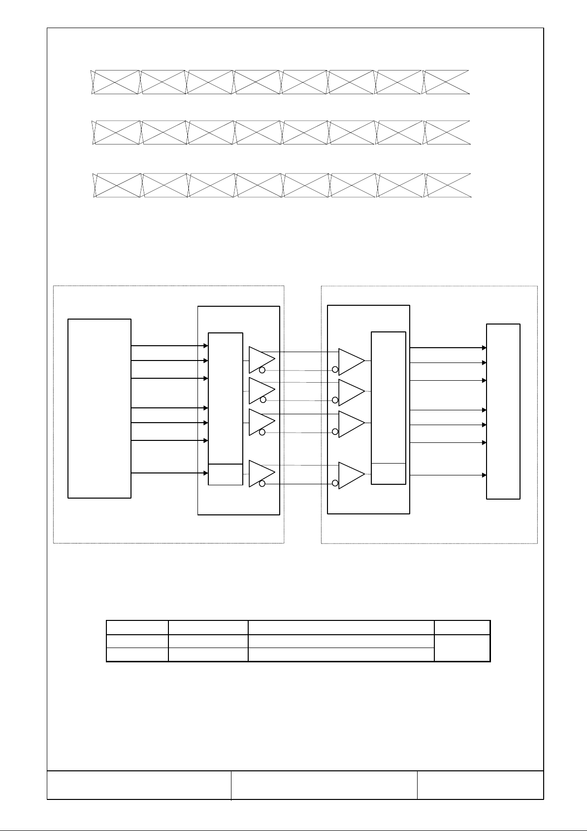
Data stream of IN0-/+, IN1-/+ and IN2-/+ for T-51410D104-FW-P-AF
GraphicController Circuit
TTLparallel to LVDS
LVDS to TTL parallel
LCD Internal Circuit
T-51410D104-FW-P-AF Module
IN0
IN1
RxOUT6 RxOUT5 RxOUT4 RxOUT3 RxOUT2
G0
RxOUT13 RxOUT12 RxOUT11 RxOUT10 RxOUT9
B1
IN2
RxOUT13 RxOUT12 RxOUT11 RxOUT10 RxOUT9
ENAB
R5
B0
NC
LVDS Interface Block Diagram
R0~R5
G0~G5
B0~B5
TIN0~TIN5
TIN6~TIN11
TIN12~TIN17
R4 R3 R2
G5 G4 G3
NC B5 B4
IN0IN0+
IN1-
RxOUT1
R1 R0
RxOUT8
G2 G1
RxOUT8
B3 B2
RxOUT0
RxOUT7
RxOUT7
RxOUT0~RxOUT5
RxOUT6~RxOUT11
RxOUT12~RxOUT17
TIN18
NC
TIN19
NC
ENAB
CLK IN
TIN20
TCLK IN
Customer systemside
PLL
DS90C*363
IN1+
IN2-
IN2+
CLKCLK+
RxOUT18
RxOUT19
RxOUT20
CLKOUT
PLL
DS90CF364
PD104SL6 moduleside
5-2) Backlight driving
Connector type :“BHR-02VS-1” of Japan Solderless Terminal MFG Co. LTD
PIN NO. Symbol Description Remark
1 VL1 Input Voltage(High)
2 VL2 Input Voltage(Low)
T-51410D104-FW-P-AF
OPTREX CORPORATION
Page 5/18
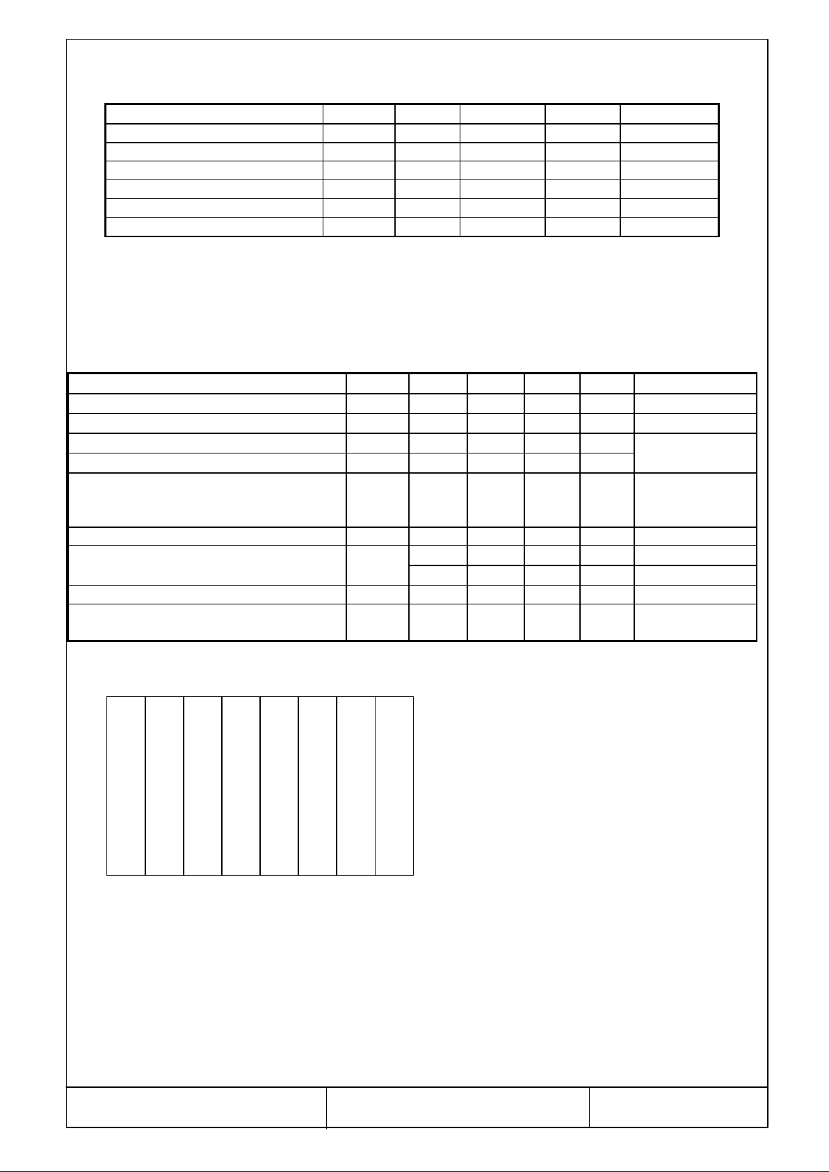
6.Absolute Maximum Ratings:
1234567
8
Parameters Symbol MIN. MAX. Unit Remark
Supply Voltage VDD -0.3 +4.0 V
Input Signals Voltage V
Backlight Driving Voltage V
Backlight Driving Frequency F
Storage Temperature T
Operating Temperature T
IN
L
L
ST
OP
-0.3 VDD+0.3 V Note 6-1
- 2000 V
0 100 KHz
-20 +70 C
0 +60 C
Note 6-1: LVDS signal
7.Electrical Characteristics
GND=0V, Ta=25C
7-1) Recommended Operating Conditions: GND = 0V,Ta = 25
Item Symbol Min. Typ. Max. Unit Remark
Supply Voltage VDD 3.0 3.3 3.6 V
Current Dissipation I
LVDS Differential input high threshold V
LVDS Differential input low threshold V
Lamp Current I
DD
TH
TL
FL
- 350 450 mA Note 7-1
- - 100 mV Note 7-2
-100 - -
3.0 7.0 - mA
Note 7-3
Note 7-5
Lamp Voltage V
Lamp Initial Voltage V
Lamp Driving Frequency F
L
SFL
L
500 550 600 Vrms Note 7-3
- 1200 - Vrms
1000
at Ta=25°C
at Ta=0°C
- 45 - KHz
Total power consumption (at IFL=7mA) - 5.01 - W Note 7-4
Note 7-1 : To test the current dissipation of VDD, using the“color bars” testing pattern
shown as below
White
1.
Yellow
2.
Cyan
3.
Green
4.
Magenta
5.
Red
6.
Blue
7.
Black
8.
℃
Idd current dissipation testing pattern
T-51410D104-FW-P-AF
OPTREX CORPORATION
Page 6/18
 Loading...