

OPTREX T-51410D104-FW-P-AE Datasheet
Rev.
Date
Page
Comment
OP T R E X
LCD Module Technical Specification
T-51410D104-FW-P-AE
Checked by (Quality Assurance Div.)
***The part number and specification are still tentative.
Checked by (Design Engineering Div.)
Prepared by (Production Div.)
Table of Contents
1. Applications................................................................................................................................................. 2
2. Features........................................................................................................................................................... 2
3. Mechanical Specifications................................................................................................................ 2
4. Mechanical Drawing TFT LCD Module............................................................................ 3
5. Input / Output Terminals................................................................................................................. 5
6. Absolute Maximum Ratings ............................................................................................................6
7. Electrical Characteristics.....................................................................................................................7
8. Power Sequence.................................................................................................................................... 13
9. Optical Characteristics..................................................................................................................... 14
10. Handling Cautions............................................................................................................................... 17
11. Reliability TEST .................................................................................................................................... 18
12. Block Diagram......................................................................................................................................... 19
13. Packing........................................................................................................................................................... 20
First Edition
Dec 17, 2001
Final Revision
******
Revision History
T-51410D104-FW-P-AE
OPTREX CORPORATION
Page 1/22
1.Application
This data sheet applies to a color TFT LCD module, T-51410D104-FW-P-AE.
T-51410D104-FW-P-AE module applies to OA product, carTV(must use Analog to Digital
drive board), which require high quality flat panel display. If you must use in high reliability
environment can’t over reliability test condition
Prime View assume no responsibility for any damage resulting from the use of the device
which dose not comply with the instructions and the precautions in these specification sheet.
2. Features
. Amorphous silicon TFT LCD panel with back-light unit
. Pixel in stripe configuration
. Slim and compact, designed for O/A application
. Display Colors:262,144 colors
. Optimum Viewing Direction:6 o’clock
. Image Up/Down, Left/Right inversion function
. +3.3V DC supply voltage for TFT LCD panel driving
. Backlight driving DC/AC inverter not included in this module
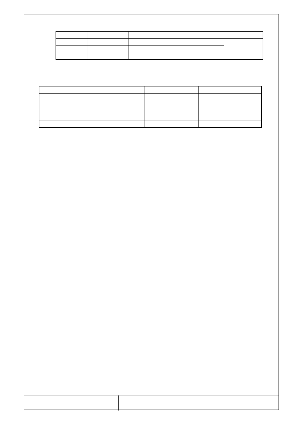
3.Mechanical Specifications
Parameter Specifications Unit
Screen Size 26.4(diagonal) cm
10.4 (diagonal) inch
Display Format
Display Colors 262,144
Active Area
Pixel Pitch
Pixel Configuration Stripe
Outline Dimension 243 (w)x185.1(H)x11(typ.) (D) mm
Weight 490(typ.), g
Back-light CCFL, 2 tubes
Surface treatment Anti-glare and hard-coating
Display mode Normally white
800×(R, G, B)×600
211.2(H)×158.4 (V)
0.264 (H)×0.264 (V)
dot
mm
mm
T-51410D104-FW-P-AE
OPTREX CORPORATION
Page 2/22
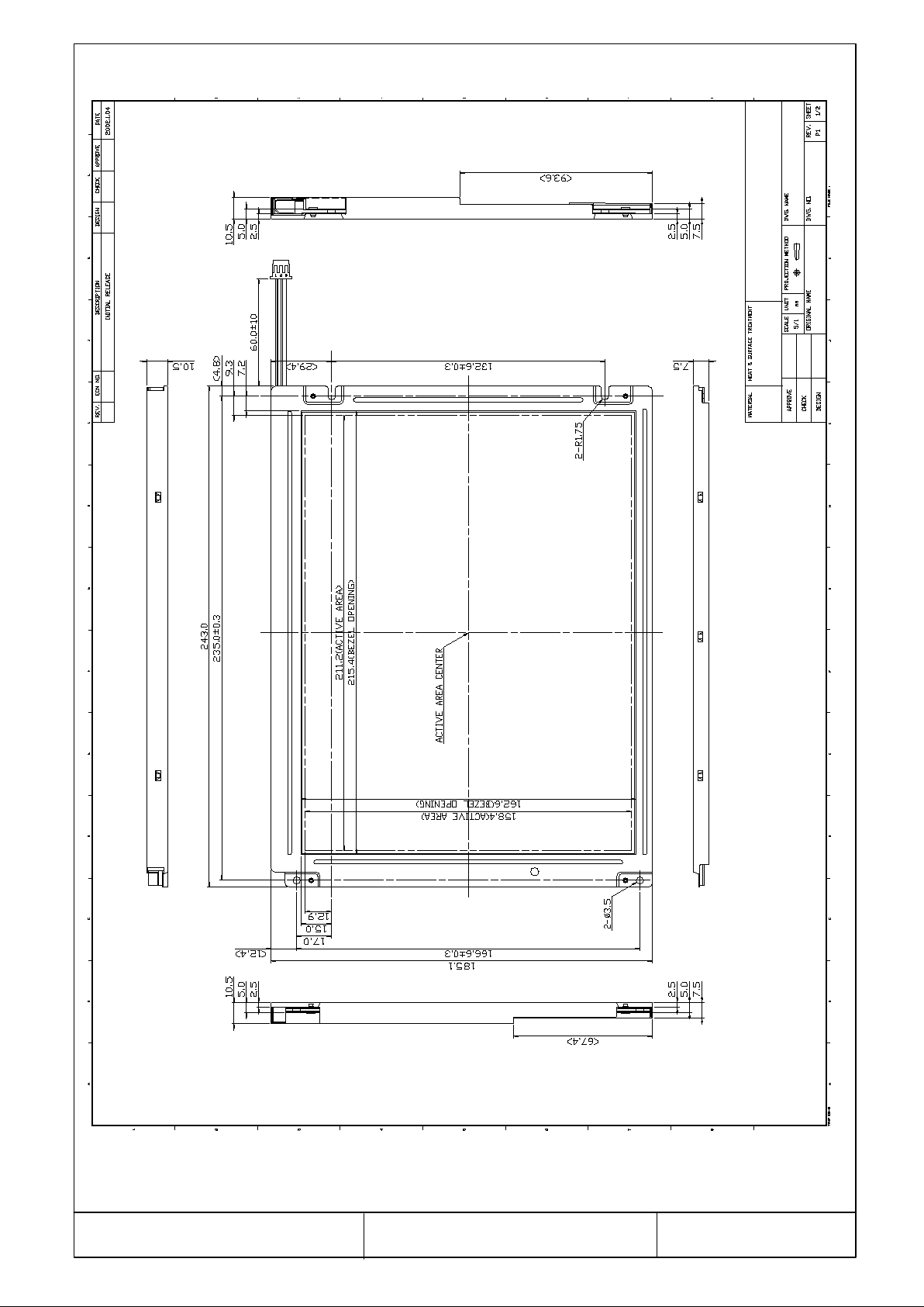
4.Mechanical Drawing of TFT-LCD Module
T-51410D104-FW-P-AE
OPTREX CORPORATION
Page 3/22
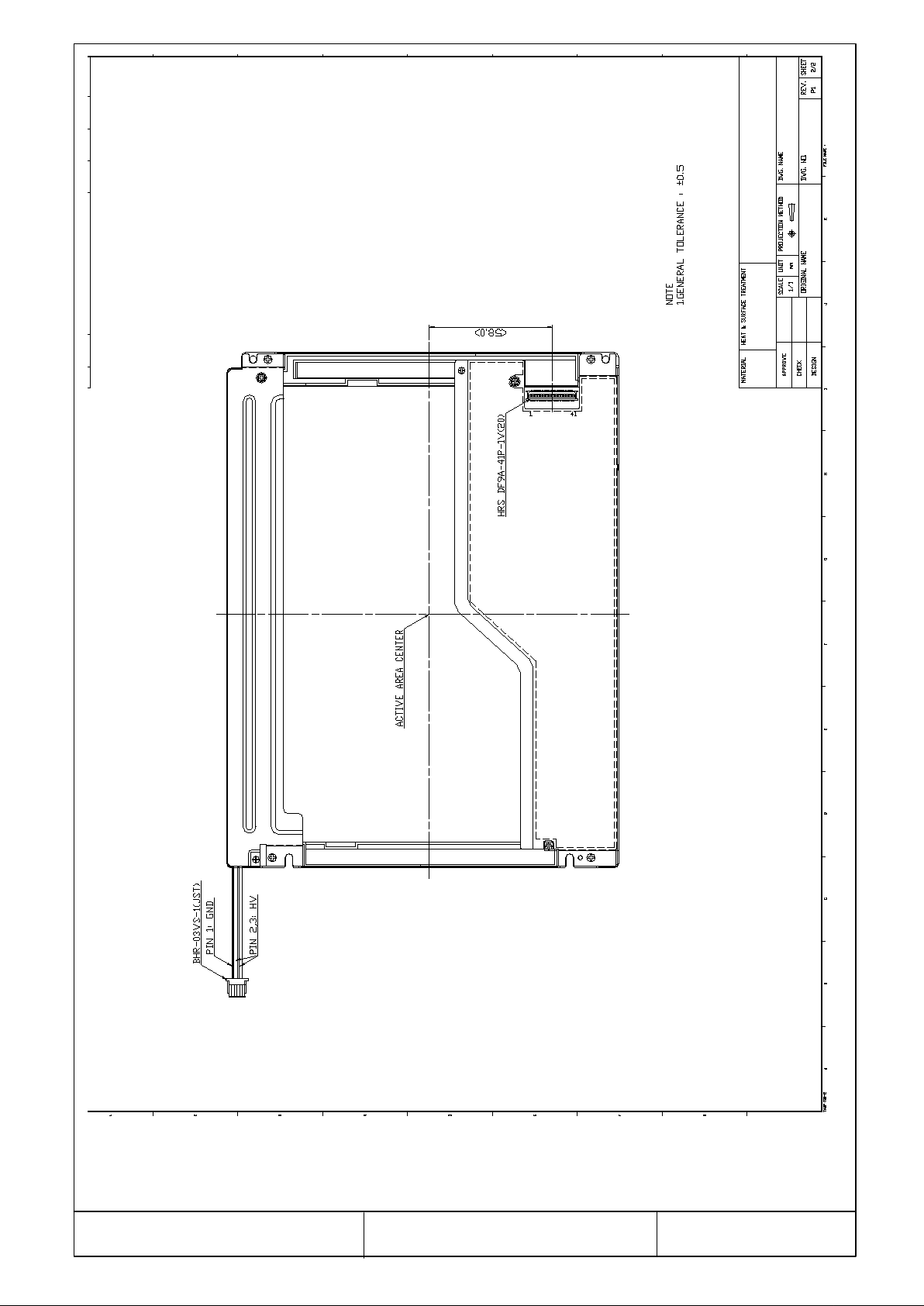
T-51410D104-FW-P-AE
OPTREX CORPORATION
Page 4/22
5.Input Terminals
5-1) TFT-LCD Panel Driving
Connector type: HIROSE, DF9B-41P-1V (or equivalent)
Pin No. Symbol Function Remark
1 GND Ground
2 CLK Clock
3 GND Ground
4 Hsync Horizontal sync
5 Vsync Vertical sync
6 GND Ground
7 GND Ground
8 GND Ground
9 R0 Red data(LSB)
10 R1 Red data
11 R2 Red data
12 GND Ground
13 R3 Red data
14 R4 Red data
15 R5 Red data(MSB)
16 GND Ground
17 GND Ground
18 GND Ground
19 G0 Green data(LSB)
20 G1 Green data
21 G2 Green data
22 GND Ground
23 G3 Green data
24 G4 Green data
25 G5 Green data(MSB)
26 GND Ground
27 GND Ground
28 GND Ground
29 B0 Blue data(LSB)
30 B1 Blue data
31 B2 Blue data
32 GND Ground
33 B3 Blue data
34 B4 Blue data
35 B5 Blue data(MSB)
36 GND Ground
37 NC No connect
38 SDS Scan direction select Note 5-1
39 Vcc Power supply
40 Vcc Power supply
41 NC No connect
Note 5-1:SDS can change scandirection .
High or open = normal scan, Low = reverse scan
T-51410D104-FW-P-AE
OPTREX CORPORATION
Page 5/22
5-2) Backlight driving
Connector type : “BHR-03VS-1” of Japan Solderless Terminal MFG Co. LTD
PIN NO. Symbol Description Remark
1 LV Ground White
2 HV Lamp power input Pink (or Gray)
3 HV Lamp power input Pink (or Gray)
6.Absolute Maximum Ratings:
Parameters Symbol MIN. MAX. Unit Remark
Supply Voltage Vcc -0.3 +3.6 V
Backlight Driving Voltage V
Backlight Driving Frequency F
Storage Temperature T
Operating Temperature T
L
L
ST
OP
- 2000 V
0 100 KHz
-20 +60 C Note 6-1
0 +50 C
Note 6-1: Humidity : 90% RH Max. at Ta £ 40C.
Maximum wet-bulb temperature is at 39Cor less at Ta > 40Cand no
condensation.
GND=0V, Ta=25C
T-51410D104-FW-P-AE
OPTREX CORPORATION
Page 6/22
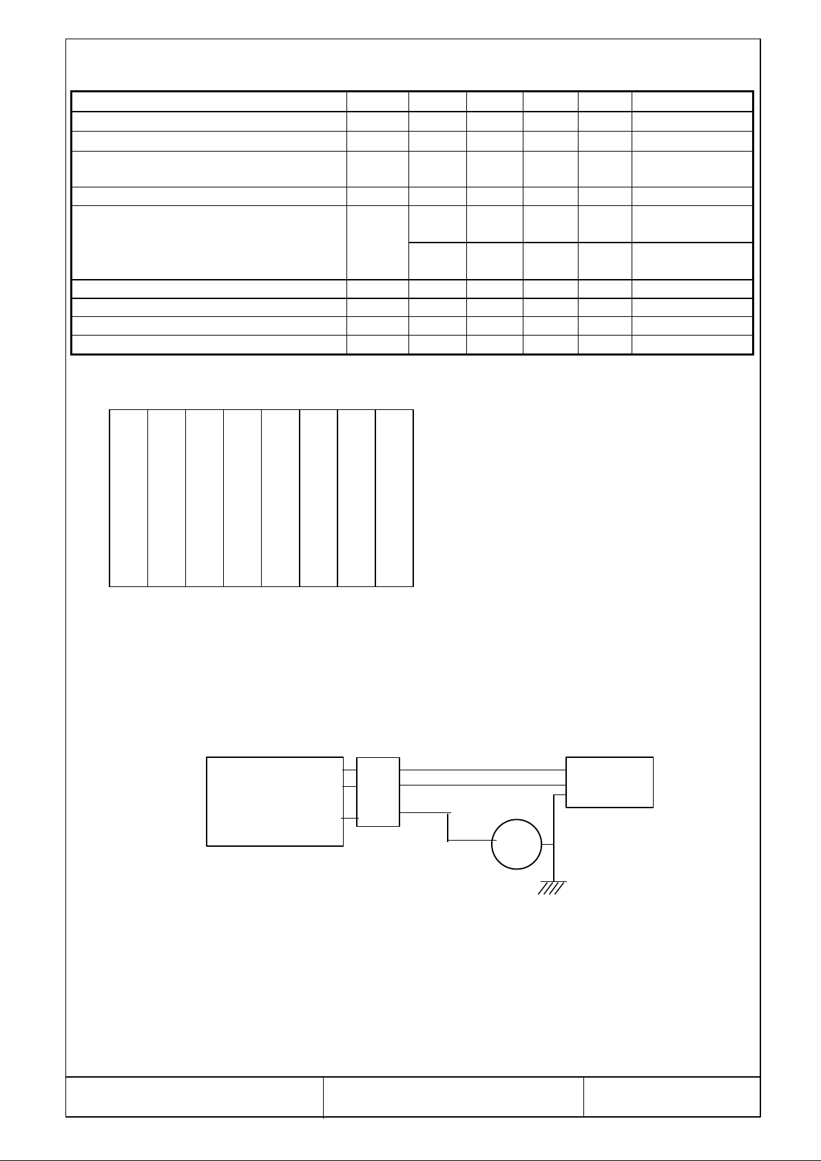
7.Electrical Characteristics
1234567
8
3 2 1
7-1) Recommended Operating Conditions: GND = 0V,Ta = 25
Item Symbol Min. Typ. Max. Unit Remark
Supply Voltage VDD 3.0 3.3 3.6 V
Current Dissipation I
Lamp Current I
Lamp Voltage V
Lamp Initial Voltage V
Lamp Driving Frequency F
Lamp power consumption 4 8 11 W Note 7-4
Lamp Life Time 30000 40000 Hrs Note 7-5
LCD Panel Life Time(MTBF) 50000 Hrs
Note 7-1 : To test the current dissipation of VDD, using the “color bars” testing pattern
shown as below
DD
FL
L
SFL
L
- 350 450 mA Note 7-1
3.0×2 7.0×2 8.0×2 mA Note 7-2
Note 7-4
400 430 530 Vrms Note 7-2
- - 875 Vrms
- - 1300
30 55 60 KHz
White
1.
Yellow
2.
Cyan
3.
Green
4.
Magenta
5.
Red
6.
Blue
7.
Black
8.
at Ta=25°C
Note 7-3
at Ta=0°C
Note 7-3
℃
Idd current dissipation testing pattern
Note 7-2 : The back-light driving waveform should be as closed to sine-wave as possible.
In order to satisfy the quality of B/L , no matter use what kind of inverter , the
output lamp current must between Min. and Max. to avoid the abnormal
display image caused by B/L.
Note 7-3 : Not including the efficiency of backlight DC/AC inverter
Note 7-4 : Lamp current is measured with current meter for high frequency as shown below
TFT-LCD
Inverter
Module
~
A
* Pin 3 isVlow
** Current meter:
Yokogawa 2016-01
Lamp current dissipation testing configuration
Note 7-5: The life time is determined as the time at which brightness of lamp is 50%
compare to that of initial value at the typical lamp current.
7-2) Input signal timing chart
T-51410D104-FW-P-AE
OPTREX CORPORATION
Page 7/22
 Loading...