

OPTREX T-51384L079J-FW-P-AA Datasheet
T-51384L079J-FW-P-AA
OPTREX CORPORATION Page-1/20
LCD Module Technical Specification
T-51384L079J-FW-P-AA
Table of Contents
1. Applications
...........................................................................................................................................................
2
2. Features
......................................................................................................................................................................
2
3. Mechanical Specifications
..........................................................................................................................
2
4. Mechanical Drawing TFT LCD Module
......................................................................................
3
5. Input / Output Terminals
...........................................................................................................................
4
6. Absolute Maximum Ratings
......................................................................................................................
6
7. Electrical Characteristics
...............................................................................................................................
6
8. Optical Characteristics
...............................................................................................................................
17
9. Handing Cautions
..........................................................................................................................................
18
10. Reliability
..............................................................................................................................................................
19
11. Block Diagram
.................................................................................................................................................
20
Checked by (Design Engineering Div.)
Checked by (Quality Assurance Div.)
Prepared by (Production Div.)
Revision History
Rev. Date Page Comment
First Edition
Jan 1, 2001
Final Revision
******
OPTREX

T-51384L079J-FW-P-AA
OPTREX CORPORATION Page-2/20
1,Application
This technical specification applies to 7.9” color TFT-LCD module1,
L079J
.The applications of
the panel are car TV, portable DVD , Video Display, m ultimedia applications and others AV
system.
2. Features
. Compatible with NTSC & PAL system
. Pixel in stripe configuration
. Slim and compact
. Dual lamp design to make high picture brightness
. Image Reversion:Up/Down and Left/Right
3. Mechanical Specifications
Parameter Specifications Unit
Screen Size 7.9 ( diagonal) inch
Display Format
1440(H)×234(V)
dot
Active Area
161.28 (H)×117.936 (V)
mm
Dot Pitch
0.112(H)×0.504 (V)
mm
Pixel Configuration Stripe
Outline Dimension 191.4 (W )×144.6 (H)×11.5 (D)(Typ.) mm
Surface treatment Anti-glare and har d coating
Weight 365±10 g
T-51384L079J-FW-P-AA
OPTREX CORPORATION Page-3/20
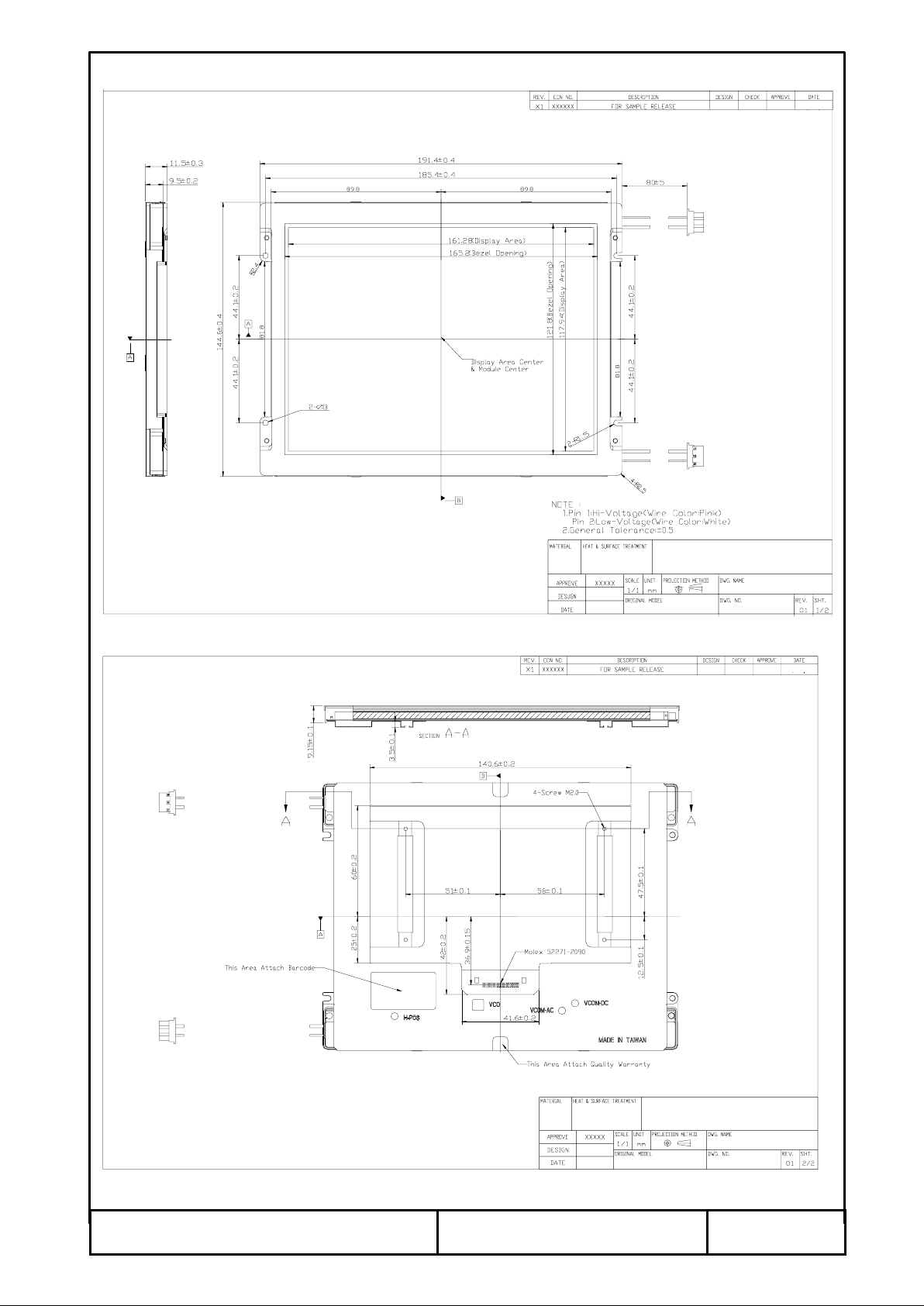
4. Mechanical Drawing of TFT-LCD Module

T-51384L079J-FW-P-AA
OPTREX CORPORATION Page-4/20
5. Input / Output Terminals
5-1) TFT-LCD Panel Driving
Pin No Symbol I/O Description Remark
1HSYI/O Horizontal Sync. Input / Output Note 5-1
2 FRP O Video Polarity Alternating Signal
3 CSY I Composite Sync. Signal Note 5-1
4VGHI Supply Voltage for Gate Driver (Hi level) Note 5-2
5VGLI Supply Voltage for Gate Dr iver ( Low level) Note 5-3
6VBI Video Signal (Blue)
7VRI Video Signal (Red)
8VGI Video Signal (Green)
9 GND I Ground
10 V
DD
I Supply voltage for Controller Note 5-4
11 V
CC
I Supply voltage for source driver Note 5-5
12 GND I Ground
13 CKC I Control pin for select I/O signal Note 5-1
14
VSY
I/O Vertical Sync. Input/ Output Note 5-1
15 PSI O Synchronize Pulse for Decoder
16 PSC O Synchronize Pulse for DC-DC Converter
17 NC -
No Connection
18 UD I UP/DOW N Cont r o l Note 5-7
19 RL I Right/Left Shift Control Note 5-6
20 NP I NTSC/PAL Input Note 5-8
Note 5-1:Pin 13 (CKC) can select the function for Pin 1 ( HSY ), Pin 3 (CSY), and Pin 14
( VSY
) .
Pin 13 (CKC)
Pin 1 ( HSY
)
Pin 3 (CSY)
Pin 14 ( VSY )
Hi HSY Out put CSY Input VSY Output
Low External Horizontal Sync Input External Clock Input
External Vertical Sync
Input
Note 5-1-1: CKC= High:
a. If CKC=1,the phase lock loop (PLL) is adopt ed in the LCD module.
b. Inputs CSY, the controller of LCD module will separate the Vertical Sync and
Horizontal Sync from CSY.
c.
Output Horizontal Sync ( HSY , Pin 1) and Vertical Sync ( VSY , Pin 14)..
d. The internal detect will detect Vert ical Sync to r e set t he vertical counter.
T-51384L079J-FW-P-AA
OPTREX CORPORATION Page-5/20
Note 5-1-2: CKC= Low (VGA mode)
a. If CKC=0, t he phase lock loop (PLL) is not adopted in the LCD module.
b. If CKC=0, the external clock input frequency of Pin 3 is 25. 175 MHz.
c. Input external Horizontal Sync (Pin 1) to synchronize the LCD module. External
Horizontal Sync and External Vertical Sync input pulse can be high going or low
going.
0. The cycle of exter nal Hor izontal Sync input is 31. 8µs. The cycle of external Vertical
Sync input is 525H.
Note 5-2:V
GH
TYP.=+17V
Note 5-3:V
GL
TYP.=-15V
Note 5-4:V
DD
TYP.=+5V
Note 5-5:V
CC
TYP.=+5V
Note 5-6 : Low (0V) for shift Right; Input Hi (+5.0V) for inverse (shift Left).
Note 5-7 : Hi (+5.0V) for DOWN; Low (0V) for UP.
Note 5-8 : PAL= LOW(0V),NTSC= Hi(+5.0V)
Low High
Note5-6 Right Left
Note5-7 Down Up
Note5-8 PAL NTSC
5-2) Backlight driving
Pin No Symbol Description Remark
1 VL1 Input terminal (Hi voltage side) Wire color: pink
2 NC NO Connection
3 VL2 Input terminal (Low voltage side)
Wire color: white
Note 5-9
Note 5-9:Low voltage side of backlight inverter connect s with Gr ound of inverter circuits.
5-3) Input / Output Connector
A)LCD Module Connector
6200-20P (Molex)
FFC Down Connector
20 Pins
Pitch:1.0 mm
B) Backlight Connector
JST BHR-03VS-1
Pin No.:3
Pitch:4 mm
Pink: High Voltage
White: Low Voltage
T-51384L079J-FW-P-AA
OPTREX CORPORATION Page-6/20
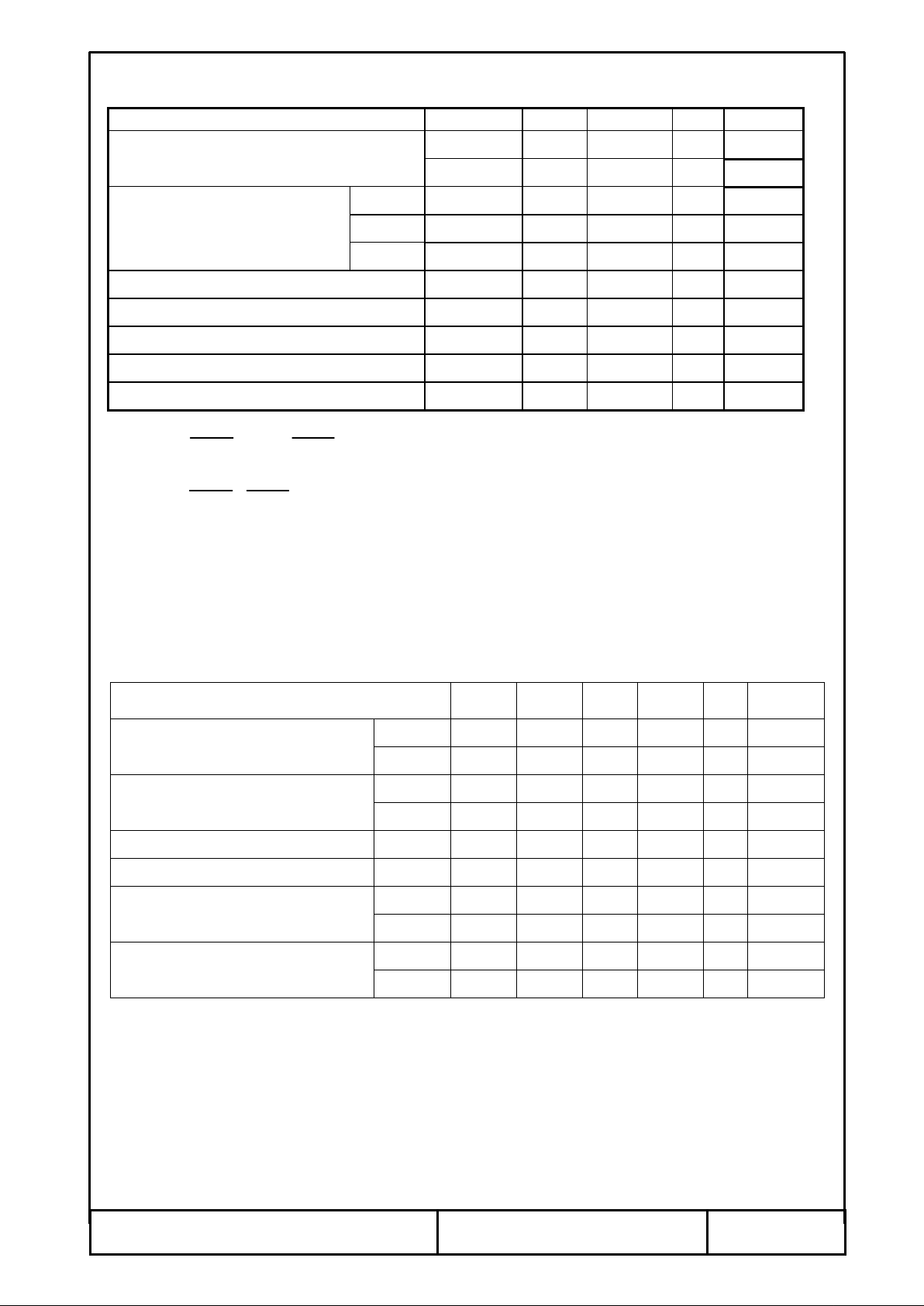
6. Absolute Maximum Ratings:
GND = 0 V, Ta = 25
℃
Parameter Symbol MIN. MAX. Unit Remark
V
CC
-0.5 7 V
Supply Voltage For Source Driver
V
DD
-0.5 7 V
V
GH- VGL
-0.3 40 V
H Level V
GH
040 V
Supply Voltage For Gate Driver
L Level
V
GL
-20
0V
Analog Signal Input Level VR,VG,V
B
-0.3 7.0 V
Digital Input Signals -0.3 5.5 V Note 6-1
Digital Output Signals -0.3 5.5 V Note 6-2
Storage Temperature -30 +80
℃
Operation Temperature -20 +70
℃
Note 6-1 : HSY , CSY, VSY , CKC,
Note 6-2 : HSY
, VSY , PSI, PSC
7. Electrical Characteristics
7-1) Recommended Operating Condit ions:
0. Driving for TFT-LCD Panel
GND = 0V, Ta = 25
℃
Parameter
Symbol MIN. Typ MA X Unit Remark
Analog V
CC
4.5 5.0 5.5 V
Supply Voltage For Source Driver
Logic V
DD
4.5 5.0 5.5 V
H level V
GH
+15 +17 +19 V
Supply Voltage For Gate Driver
L level V
GL
-16 -15 -14 V
Supply Voltage For controller
V
DD
4.5 5.0 5.5 V
Analog Signal input Level Amplitud
0.3 V
CC-
0.3 V
H level V
IH
0.7 V
DD
-VDDV
Digital input voltage
L level V
IL
-0.3 - 0.3 V
DD
V
H level V
OH
0.7 V
DD
-VDDV
Digital output voltage
L level V
OL
-0.3 - 0.3 V
DD
V
 Loading...