

OPTREX T-51383L070J-FW-P-AA Datasheet
T-51383L070J-FW-P-AA
OPTREX CORPORATION Page-
1/22
LCD Module Technical Specification
T-51383L070J-FW-P-AA
Table of Contents
1. Applications
...........................................................................................................................................................
2
2. Features
.....................................................................................................................................................................
2
3. Mechanical Specifications
.........................................................................................................................
2
4. Mechanical Drawing TFT LCD Module
.....................................................................................
3
5. Input / Output Terminals
..........................................................................................................................
4
6. Absolute Maximum Ratings
.....................................................................................................................
6
7. Electrical Characteristics
...............................................................................................................................
6
8. Power Sequence
.........................................................................................................................................
15
9. Optical Characteristics
................................................................................................................................
16
10. Handing Cautions
...........................................................................................................................................
17
11. Reliability TEST
.............................................................................................................................................
22
12. Block Diagram
....................................................................................................................................................
23
Checked by (Design Engineering Div.)
Checked by (Quality Assurance Div.)
Prepared by (Production Div.)
Revision History
Rev. Date Page Comment
First Edition
Jan 1, 2001
Final Revision
******
OPTREX
T-51383L070J-FW-P-AA
OPTREX CORPORATION Page-
2/22
1. Application
This technical specification applies to 7.0” color TFT-LCD module. The applications of the
panel are car TV, portable DVD,GPS, m ultimedia applications and others AV system.
2. Features
. Compatible with NTSC & PAL system
. Pixel in stripe configuration
. Slim and compact
. High Brightness
. Image Reversion:Up/Down and Left/Right
. Multi Video Display Mode
3. Mechanical Specifications
Parameter Specifications Unit
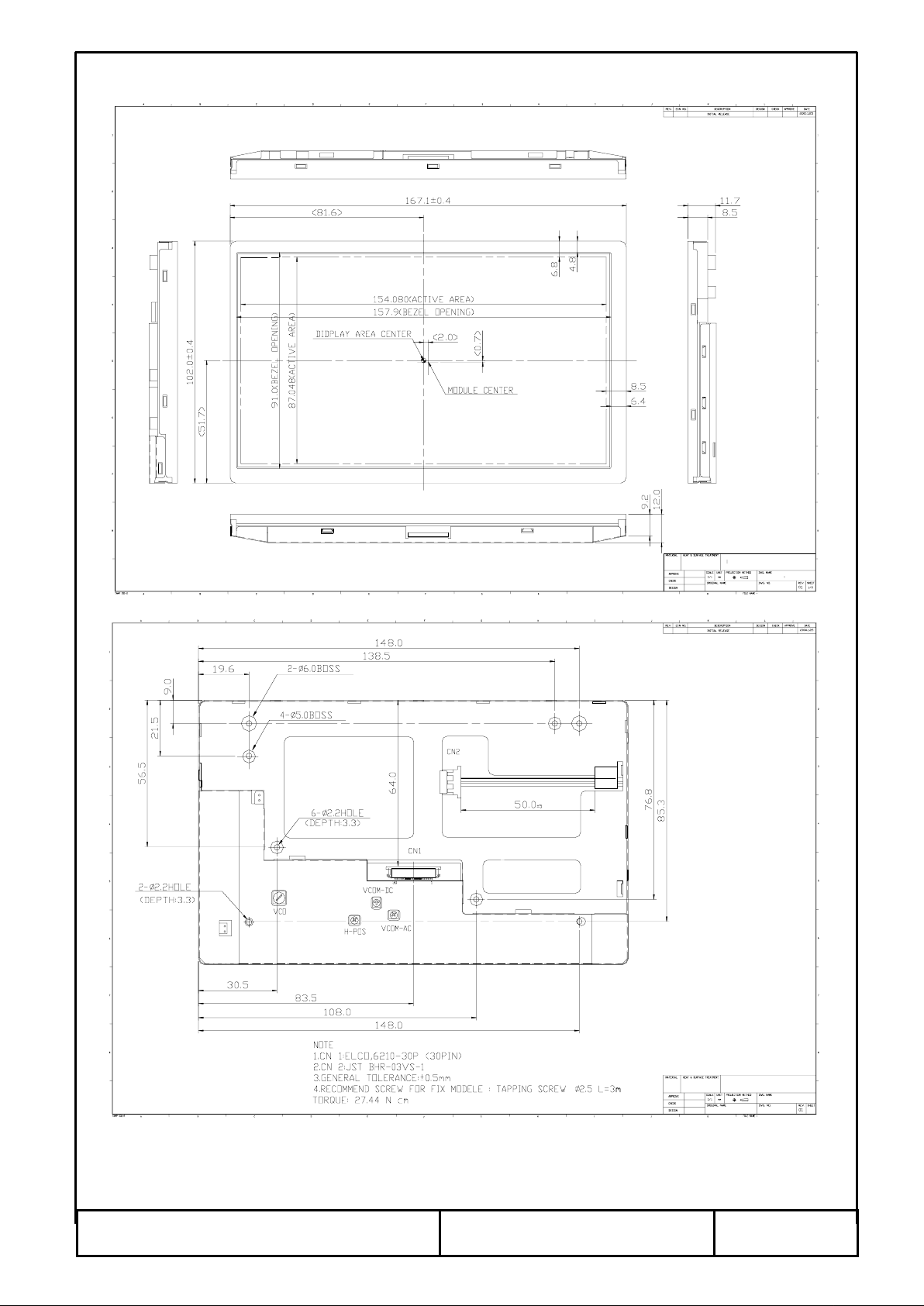
Screen Size 7.0 (16:9 diagonal) inch
Display Format
1440 (H) ×234(V)
dot
Active Area
154.08 (H)×87.05 (V)
mm
Dot Pitch
0.107(H)×0.372 (V)
mm
Pixel Configuration Stripe
Outline Dimension 167.1 (W )×102.0 (H)×12.0 (D)(typ.) mm
Surface Treatment Anti-Glare and Hard Coating
Weight
205±10
g
T-51383L070J-FW-P-AA
OPTREX CORPORATION Page-
3/22
4. Mechanical Drawing of TFT-LCD Module
T-51383L070J-FW-P-AA
OPTREX CORPORATION Page-
4/22
5. Input / Output Terminals
5-1) TFT-LCD Panel Driving
The interface connector is 6210-30P Series manufactured by ELCO or equivalent.
(0.5mm pitch 30 pin)
The connector interface pin assignments are listed in the Table below.
Pin No
Symbol
I/O Description Remark
1
PSI
O Synchronize Pulse for Decoder
2
V
R
I Red Video Input
3
V
G
I Green Video Input
4
V
B
I Blue Video Input
5
GND
I Ground
6
CSY
I Composite Sync Input
7
NC
No Connection
8
NC
No Connection
9
NC
No Connection
10
NC
No Connection
11
MODE 1
I Display mode selection pin 1 (refer to 5.2)
12
MODE 2
I Display mode selection pin 2 (refer to 5.2)
13
MODE 3
I Display mode selection pin 3 (refer to 5.2)
14
GND
I Ground
15
BLK
O Video Signal Mask Timing Output
16
HSY
O Horizontal Sync Output
17
VSY
O Vertical Sync Output
18
V
DD
I Input Voltage For Logic/Logic Voltage For Source Driver
19
NC
No Connection
20
FRP
O Video Polarity Control Signal
21
GND
I Ground
22
U/D
I Scanning Direction : (Low : Normal , High : Reverse)
23
L/R
I Scanning Direction : (Low : Normal , High : Reverse)
24
N/P
I NTSC/PAL Selection Signal(Low : PAL , Hig h : NTSC)
25
NC
No Connection
26
NC
No Connection
27
GND
I Ground
28 V
CC
I Analog Voltage For Source Driver/Logic Voltage For Gate
29 V
GH
I Positive Voltage For Gate Driver
30 V
GL
INegative Voltage For Gate Driver
T-51383L070J-FW-P-AA
OPTREX CORPORATION Page-
5/22
5.2)Display Mode
NO:11 NO:12 NO:13
Display Mode
Display (Input Signal
of 4:3 Aspect Ratio)
Mode 1 Mode 2 Mode 3
Note
Full
Low
Low Low
Input Video Signals Are
Displayed In Full Screen.
Normal
Center
High Low Low
Input Video Signals Are
Displayed In The Center
Screen.(4:3 Aspect Ratio)
Zoom 1 High High Low
Input Video Signal Of
Central 176 Lines Are
Display In Full
Screen.(Vertically Extension)
Wide Low High Low
Input Video Signals Are
Displayed In Full Screen.
(Horizontal Modification)
Normal Left High Low High
Input Video Signals Are
Display In the Left Screen.
(4:3 Aspect Ratio)
Normal Right
Low
High High
Input Video Signals Are
Display In the Right Screen.
(4:3 Aspect Ratio)
Zoom 2 Low Low High
I
nput Video Signal Of
Central 204 Lines Are
Display In Full
Screen.(Vertically Extension
Zoom 3
High
High High
Same As Zoom 2 Mode
Vertically Offset Centered
T-51383L070J-FW-P-AA
OPTREX CORPORATION Page-
6/22
6
Absolute Maximum Ratings:
The followings are maximum values , which if exceeded, may cause faulty operat ion or dam age
to the unit.
Parameter Symbol MIN. MAX. Unit Remark
V
CC
-0.5 7 V
Supply Voltage For Source Driver
V
DD
-0.5 7 V
V
GH- VGL
-0.3 40 V
H Level V
GH
040 V
Supply Voltage For Gate Driver
L Level
V
GL
-20
0V
Analog Signal Input Level VR,VG,V
B
-0.3 7.0 V Note 6-1
Digital Input Signals -0.3 5.5 V
Digital Output Signals -0.3 5.5 V
Storage Temperature -30 +80
℃
Operation Temperature -20 +70
℃
Note 6-2
Notes:6-1 Analog Input Voltage means VR,VG,VB.
Notes:6-2 Operating Tem perature define that contrast, response time, other display
optical character are Ta=+25.
7
Electrical Characteristics
7-1) Recommended Driving condition for TFT-LCD panel
Parameter
Symbol MIN. Typ MAX Unit Remark
Analog V
CC
4.5 5.0 5.5 V
Supply Voltage For Source
Driver
Logic V
DD
4.5 5.0 5.5 V
H level V
GH
+15 +17 +19 V
Supply Voltage For Gate Driver
L level V
GL
-16 -15 -14 V
Supply Voltage For controller
V
DD
4.5 5.0 5.5 V
Analog Signal input Level
Amplitude 0.3 V
CC-
0.3 V
H level V
IN
0.7
-VDDV
Digital input voltage
L level V
IL
-0.3 - 0.3 V
DD
V
H level V
OH
0.7
-VDDV
Digital output voltage
L level V
OL
-0.3 - 0.3 V
DD
V
7-2) Backlight driving & Power Consumpt ion
Pin No Symbol Description Remark
1 VL1 Input terminal (Hi voltage side) Wire color: pink
2 NC No Connection
3 VL2 Input ter minal (Low voltage side) Wire color: white Note 7-1
T-51383L070J-FW-P-AA
OPTREX CORPORATION Page-
7/22
Note 7-1:Low voltage side of backlight inverter connect s with Gr ound of inverter circuits.
Recommended Driving condition for backlight Ta= 25
℃
Parameter Symbol Min. Typ. Max. Unit Remark
Lamp voltage V
L
810 Vrms IL=6mA
Lamp current I
L
4.5 6 7 mA
Lamp frequency P
L
35 60 KHz Note 7-2
Kick-off voltage(25
℃
)
Vs TBD TBD 1095 Vrms Note 7-3
Kick-off voltage(0
℃
)
Vs TBD TBD 1340 Vrms Note 7-3
Note 7-2 : The waveform of lam p driving voltage should be as closed to a perfect sine wave as
possible.
Note 7-3 : The Kick-off times≧1sec.
Power Consumption Ta= 25
℃
Parameter Symbol Conditions TYP. MAX Unit Remark
Supply current for Gate Dr iver ( Hi level) I
GH
V
GH
=
+17V
0.15 0.2 mA
Supply current for Gate Dr iver ( Low level) I
GL
V
GL
=
-15V
20 50 mA
Supply current for Source Driver I
CC
VCC = +5V
20 30 mA
Supply current for controller I
DD
VDD = +5V
20 30 mA
LCD Panel Power Consumption 0.50 W Note 7-4
Backlight Lamp Power Consumption 4.86 W Note 7-5
Note 7-4:The power consumption for backlig ht is not included.
Note 7-5:Backlight lamp power consumption is calculated by I
L
×
V
L
.
7-4) Input / Output Connector
A) LCD Module Connector
The interface connector is 6210-30p Ser ies m anufactured by Elco or equivaleut
(0.5mm pitch 30pin)
B) Backlight Connector, JST BHR-03VS-1. Pin No.:3, Pitch:4 mm
7-5) Pixel Arrangement and Output Interface Pin
123456
1438 1439 1440
1RGBRGB RGB
2RGBRGB RGB
3RGBRGB RGB
233RGBRGB RGB
234RGBRGB RGB
 Loading...