

OPTREX T-51382D064J-FW-P-AA Datasheet
T-51382D064J-FW-P-AA (AA) No. 2002-0221 OPTREX CORPORATION Page 1/24
LCD Module Technical Specification
T-51382D064J-FW-P-AA
NO. ITEM PAGE
- Contents 1
1 Application 2
2 Features 2
3 Mechanical Specifications 2
4 Mechanical Drawing of TFT-LCD module 3
5 Input / Output Terminals 4
6 Absolute Maximum Ratings 6
7 Electrical Characteristics 6
8 Optical Characteristics 15
9 Handling Cautions 17
10 Reliability Test 18
11 Indication of Label 18
12 Block Diagram 19
13 Standard 20
14 Packing 23
- Revision History 24
Checked by (ACI Engineering Div.)
Checked by (Quality Assurance Div.)
Approved by (Production Div.)
Prepared by (Production Div.)
Type No.
Sep 18, 2002
OPTREX
First Edition
Final Revision
******
T-51382D064J-FW-P-AA (AA) No. 2002-0221 OPTREX CORPORATION Page 2/24
1. Application
This product applies computer peripheral , industrial meter , image communication and
multi-media.
2. Features
. Compatible with VGA-480 , VGA-400 , VGA-350 and free format.
. Pixel in stripe configuration
. Slim and compact
. Display Colors : 262,144 colors
. Image Reversion : Up/Down and Left/Right
. Active area / Outline area = 62.3 %
. Viewing Direction : 6 o’clock
. Backlight lamps are Replaceable
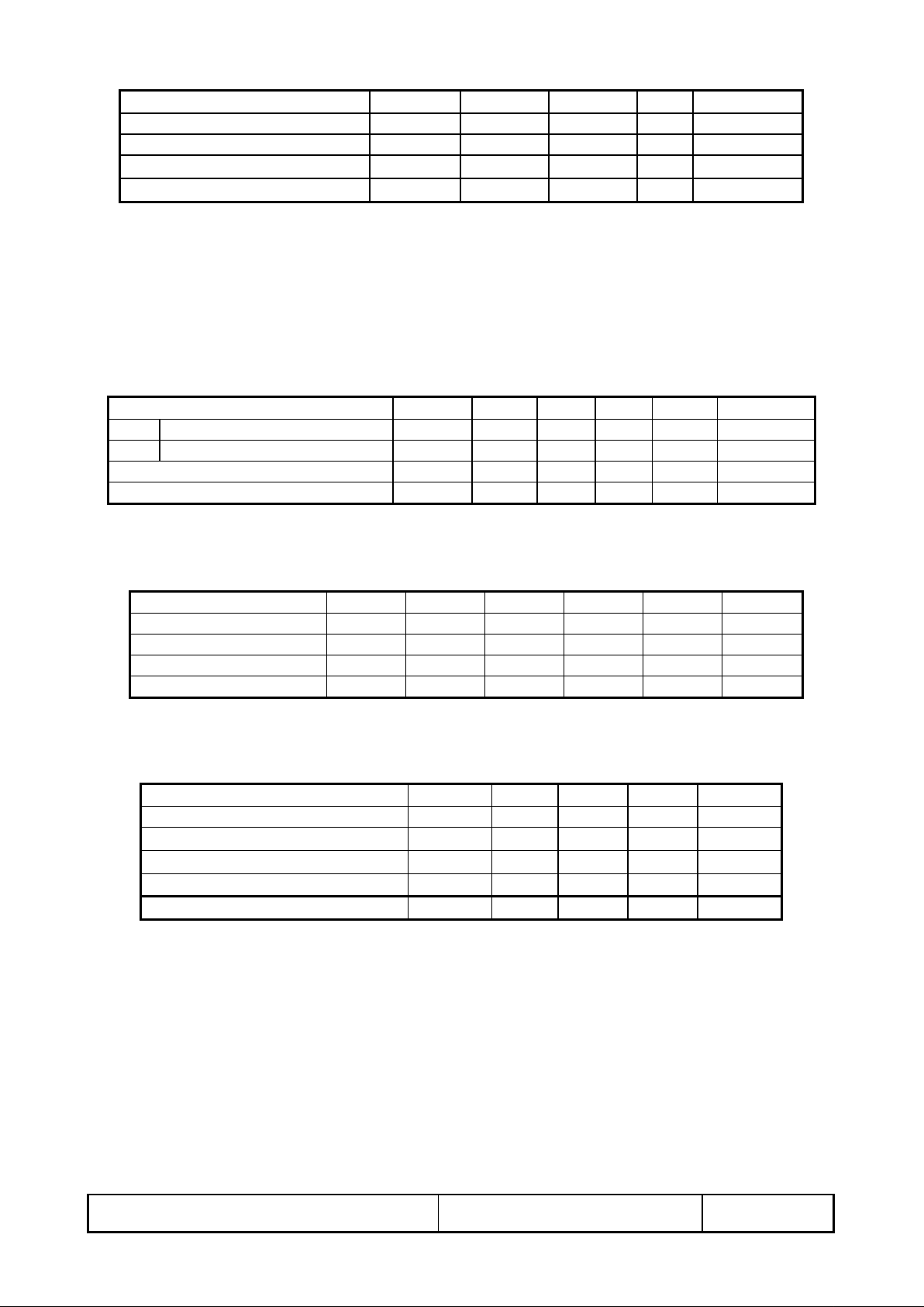
3. Mechanical Specifications
Parameter Specifications Unit
Screen Size 6.4 (diagonal) inch
Display Format
640×R, G, B×480
dot
Active Area
129.6(H)×97.44 (V)
mm
Dot Pitch
0.0675 (H)×0.203 (V)
mm
Pixel Pitch
0.203 (H)×0.203 (V)
mm
Pixel Configuration Stripe
Outline Dimension See Mechanical Drawing mm
Weight 335±10 g
T-51382D064J-FW-P-AA (AA) No. 2002-0221 OPTREX CORPORATION Page 3/24
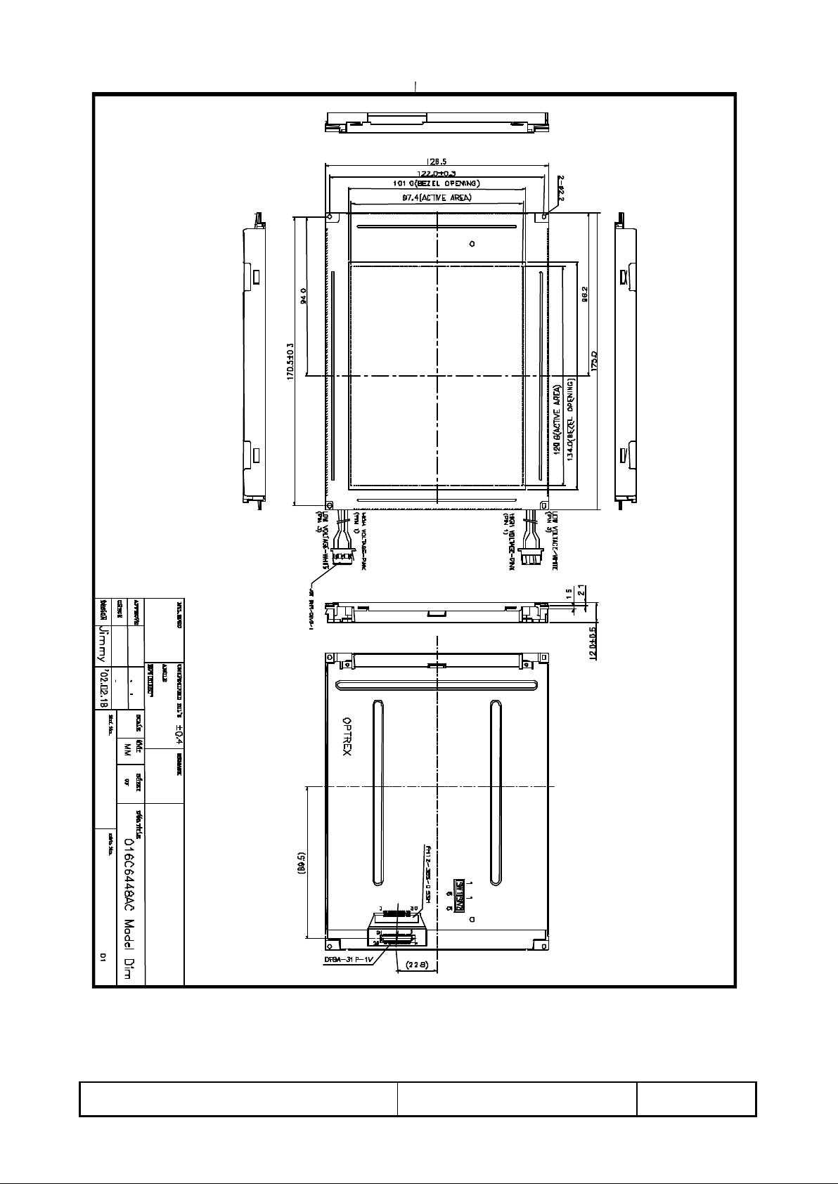
4. Mechanical Drawing of TFT-LCD Module
T-51382D064J-FW-P-AA (AA) No. 2002-0221 OPTREX CORPORATION Page 4/24
5. Input / Output Terminals
5-1) TFT-LCD Panel Driving
Pin No. Symbol Function Remark
1 GND Ground (0V)
2 CLK Clock Signal for Sampling Image Digital Data
3 Hsync Horizontal Synchronous Signal Note 5-1
4 Vsync Vertical Synchronous Signal Note 5-1
5 GND Ground (0V)
6 R0 Red Image Data Signal (LSB)
7 R1 Red Image Data Signal
8 R2 Red Image Data Signal
9 R3 Red Image Data Signal
10 R4 Red Image Data Signal
11 R5 Red Image Data Signal (MSB)
12 GND Ground (0V)
13 G0 Green Image Data Signal (LSB)
14 G1 Green Image Data Signal
15 G2 Green Image Data Signal
16 G3 Green Image Data Signal
17 G4 Green Image Data Signal
18 G5 Green Image Data Signal (MSB)
19 GND Ground (0V)
20 B0 Blue Image Data Signal (LSB)
21 B1 Blue Image Data Signal
22 B2 Blue Image Data Signal
23 B3 Blue Image Data Signal
24 B4 Blue Image Data Signal
25 B5 Blue Image Data Signal (MSB)
26 GND Ground (0V)
27 DENB Disable
28 VCC DC +5.0V Power Supply
29 VCC DC +5.0V Power Supply
30 R/L Horizontal Image Shift-direction Select Signal Note 5-2
31 U/D Vertical Image Shift-direction Select Signal Note 5-3
Note 5-1: The TFT-LCD module is compatible with four kinds of VGA timing. They are
VGA-480,VGA-400,VGA-350 and freedom mode . The polarization of Hsync and
Vsync determine the timings.
VGA-480 VGA-400 VGA-350 Freedom Mode
Hsync Polarization Negative Negative Positive Positive
Vsync Polarization Negative Positive Negative Positive

T-51382D064J-FW-P-AA (AA) No. 2002-0221 OPTREX CORPORATION Page 5/24
Note 5-2: R/L is the Right/Left shift signal.
(1) R/L= High, U/D= Low (2) R/L= Low, U/D= Low
Note 5-3: U/D is the Up/Down shift signal.
(1) R/L= High, U/D= Low (2) R/L= High, U/D= High
5-2) Backlight driving
Pin No Symbol Description Remark
1 VL1 Input terminal (Hi voltage side)
2 NC No Connection
3 VL2 Input terminal (Low voltage side) Note 5-4
Note 5-4: Low voltage side of backlight inverter connects with ground of inverter circuits.
5-3) Input / Output Connector
(A) LCD module connector (Reference)
DF9A-31P-1V
(B) Backlight Connector
JST BHR-03VS-1
Pin No.: 3
Pitch: 4 mm
Red: High Voltage
White: Low Voltage
T-51382D064J-FW-P-AA (AA) No. 2002-0221 OPTREX CORPORATION Page 6/24
6. Absolute Maximum Ratings:
GND=0V, Ta=25°C
Parameters Symbol MIN. MAX. Unit Remark
+5V Supply Voltage V
CC
0.0 +6.0 V
Input Signals Voltage V
sig
-0.3 VCC+0.3 V Note 6-1
Storage Temperature T
stg
-30 +70
°C
Operating Temperature T
opa
-20 +70
°C
Note 6-1: Input signals include CLK , Hsync , Vsync , DENB , R[0:5] , G[0:5] and B[0:5].
7. Electrical Characteristics
7-1) Recommended Operating Conditions:
A) Driving for TFT-LCD panel
GND = 0V , Ta = 25°C
Parameters Symbol Min. Typ. Max. Unit Remark
+5V Supply Voltage V
CC
+4.75 +5.0 +5.25 V
Supply Input Ripple Voltage V
CCRP
0.1 Vp-p VCC=+5V
Input Signals Voltage (High) V
IH
+2.6 V
Input Signals Voltage (Low) V
IL
+0.5 V
(B) Driving for backlight
Ta = 25°C
Item Symbol Min. Typ. Max. Unit Remark
Tube Current I
f
- 6 - mA
Tube Voltage V
L
- 380 - Vrms
Oscillation - 35 - KHz
Lamp Life Time - 20,000 - Hr
7-2) Power Consumption
Parameters Symbol Typ. Max. Unit Remark
+5V Current Dissipation I
CC
260 300 mA
Input Signals Current (High) I
IH
100
µA
VIH =+5V
Input Signals Current (Low) I
IL
100
µA
VIL =0V
LCD Panel Power Consumption 1.3 W Note 7-1
Backlight Power Consumption 4.56 W Note 7-2
Note 7-1 : The power consumption of backlight is not included.
Note 7-2 : Backlight lamp power consumption is calculated by I
L
×
VL.
T-51382D064J-FW-P-AA (AA) No. 2002-0221 OPTREX CORPORATION Page 7/24
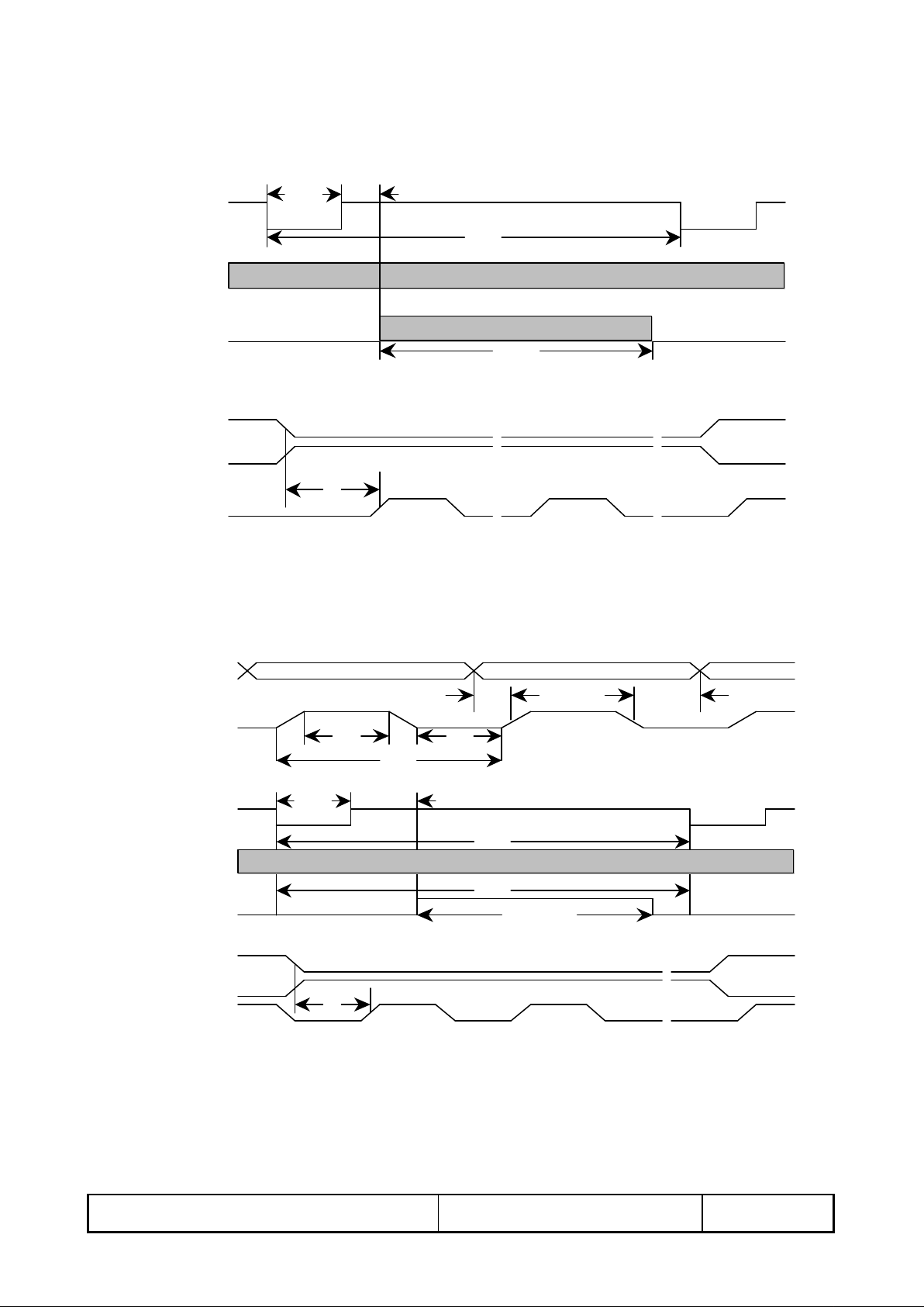
7-3) Input / Output signal timing chart
Parameters Symbol Format Min. Typ. Max. Unit Note
Frequency Fc=1/Tc All 25.175 MHz Note 7-3
Clock High Time Tckh All 10 ns
Low Time Tckl All 10 ns
Periodic = Line Thp All 31.778
µs
Note 7-3
Hsync 800 1024 clock Note 7-3
Pulse Width Thpw All 2 96 200 clock
Back Porch Thbp All 2 48 64 clock
VGA-480 515 525 1024 line Note 7-3
Periodic = Frame Tvp VGA-400 447 449 1024 line Note 7-3
VGA-350 447 449 1024 line Note 7-3
Vsync Freedom
Mode
1024 line
Pulse Width Tvpw All 1 2 line
Back Porch Tvbp All 1 64 line
Data Setup Time Tds All 10 ns
Hold Time Tdh All 10 ns
Periodic = Line Tep All 800 1024 clock
Pulse Width (H) Tepw All 2 640 800 clock
DENB VGA-480 480 480 line
Display Line No(V) Tvd VGA-400 400 400 line
VGA-350 350 350 line
Freedom
Mode
480 line
Horizontal Display Periodic Thd All 640 640 640 clock
Hsync-CLK
Phase Difference
Thc All 10 Tc-10 ns
Vsync-Hsync
Phase Difference
Tvh All 1 Thp-1 clock
Note 7-3: Tc is the period of sampling clock. In case of low-frequency, the image-flicker may
occur.
T-51382D064J-FW-P-AA (AA) No. 2002-0221 OPTREX CORPORATION Page 8/24
7-4) Display Time Range
(1) Vertical Timing :
(2) Horizontal Timing :
Tvbp
Tvd
Vsync
Hsync
DENB
Tvp
Tvpw
Vsync
(Negative)
(Positive)
Tvh
Hsync
Tds
Thp
Tc
TcklTckh
Hsync
CLK
DENB
CLK
Thpw
Tep
Tepw = Thd
Hsync
(Negative)
(Positive)
Thc
CLK
Tdh
R0~R5
G0~G5
B0~B5
Thbp
 Loading...