

OPTREX F-51430NFU-FW-AA Datasheet
F-51430NFU-FW-AA (AA) No. 2001-0115 OPTREX CORPORATION Page 1/20
LCD Module Technical Specification
F-51430NFU-FW-AA
Table of Contents
1. General Specifications
.................................................................................................................... 2
2. Electrical Specifications
.................................................................................................................. 3
3. Optical Specifications
....................................................................................................................... 9
4. I/O Terminal
........................................................................................................................................ 11
5. Test
......................................................................................................................................................... 14
6. Appearance Standards
................................................................................................................. 15
7. Code System of Production Lot
................................................................................................ 18
8. Type Number
...................................................................................................................................... 18
9 . Applying Precautions
...................................................................................................................... 18
10. Precautions Relating Product Handling
............................................................................... 19
11. Warranty
............................................................................................................................................. 20
Checked by (Design Engineering Div.)
Checked by (Quality Assurance Div.)
Approved by (Production Div.)
Prepared by (Production Div.)
Revision History
Rev. Date Page Comment
Type No.
Jun 2 1 , 2001
OPTREX
First Edition
Final Revision
******

F-51430NFU-FW-AA (AA) No. 2001-0115 OPTREX CORPORATION Page 2/20
1. General Specifications
Operating Temp. : min. 0°C ~max. 50°C
Storage Temp. : min. -20°C ~max. 60°C
Dot Pixels : 640 (W) × 480 (H) dots
Dot Size : 0.27 (W) × 0.27 (H) mm
Dot Pitch : 0.30 (W) × 0.30 (H) mm
Viewing Area : 196.0 (W) × 148.0 (H) mm
Outline Dimensions : 260.0* (W) × 174.0 (H) × 8.5 max. (D) mm
* Without CFL Cable
Weight : 410g max.
LCD Type : NTD-21140
( F-STN / Black &White-mode / Transmissive )
Viewing Angle : 12:00
Data Transfer : 4-bit parallel data transfer × 2
Backlight : Cold Cathode Fluorescent Lamp (CFL) × 1
Drawings : Dimensional Outline UE-210259-00
F-51430NFU-FW-AA (AA) No. 2001-0115 OPTREX CORPORATION Page 3/20
2. Electrical Specifications
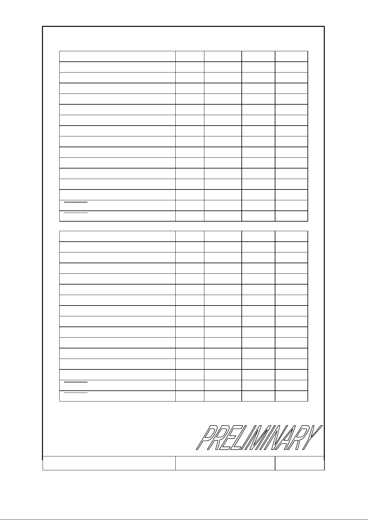
2.1. Absolute Maximum Ratings
VSS=0V
Parameter Symbol Conditions Min. Max. Units
Supply Voltage
(Logic)
VCC-V SS - -0.3 7.0 V
Supply Voltage
(LCD Drive)
VHH-V SS - -0.3 30.0 V
Input Voltage VI - -0.3 VCC+0.3 V
2.2. DC Characteristics
Ta=25°C , V SS=0V
Parameter Symbol Conditions Min. Typ. Max. Units
Supply Voltage
(Logic)
VCC-V SS - 2.5 - 5.5 V
Supply Voltage
(LCD Drive)
VHH-V SS Shown in 3.1 V
High Level
Input Voltage
VIH VCC=2.5~5.5V 0.8×VCC - VCC V
Low Level
Input Voltage
VIL VCC=2.5~5.5V 0 - 0.2×VCC V
Supply Current
ICC VCC-V SS=5.0V - 14.0 25.0 mA
IHH VHH-V SS=21.6V - 9.0 20.0 mA
F-51430NFU-FW-AA (AA) No. 2001-0115 OPTREX CORPORATION Page 4/20
2.3. AC Characteristics
VCC=2.5 ~4 .5V
Parameter Symbol Min. Max. Units
Shift Clock P eriod
t
WCK 125 - ns
Shift Clock “H” Pulse Width
t
WCKH 51 - ns
Shift Clock “L” Pulse Width
t
WCKL 51 - ns
Data Setup Time
t
DS 30 - ns
Data Hold Time
t
DH 40 - ns
Latch Pulse “H” Pulse Width
t
WLPH 51 - ns
Shift Clock Rise to Latch Pulse Rise
t
LD 0 - ns
Shift Clock Fall to Latch Pulse Fall
t
SL 51 - ns
Latch Pulse Rise to Shift Clock Rise
t
LS 51 - ns
Latch Pulse Fall to Shift Clock Rise
t
LH 51 - ns
Input Signal Rise,Fall Time
t
r, tf - 50 Note.1 ns
Data Setup Time
t
SU 30 - ns
Data Hold Time
t
H 50 - ns
DISPOFF Removal Time
t
S D 100 - ns
DISPOFF Enable Pulse Width
t
WDL 1.2 -
µ
s
VCC=4. 5 ~5.5V
Parameter Symbol Min. Max. Units
Shift Clock P eriod
t
WCK 71 - ns
Shift Clock “H” Pulse Width
t
WCKH 23 - ns
Shift Clock “L” Pulse Width
t
WCKL 23 - ns
Data Setup Time
t
DS 10 - ns
Data Hold Time
t
DH 20 - ns
Latch Pulse “H” Pulse Width
t
WLPH 23 - ns
Shift Clock Rise to Latch Pulse Rise
t
LD 0 - ns
Shift Clock Fall to Latch Pulse Fall
t
SL 25 - ns
Latch Pulse Rise to Shift Clock Rise
t
LS 25 - ns
Latch Pulse Fall to Shift Clock Rise
t
LH 25 - ns
Input Signal Rise,Fall Time
t
r, tf - 50 Note.1 ns
Data Setup Time
t
SU 30 - ns
Data Hold Time
t
H 50 - ns
DISPOFF Reoval Time
t
S D 100 - ns
DISPOFF Enable Pulse Width
t
WDL 1.2 -
µ
s
Note.1 : (
t
CK – twckll - twckl)/2 is the maximum in case of high speed operation.
F-51430NFU-FW-AA (AA) No. 2001-0115 OPTREX CORPORATION Page 5/20
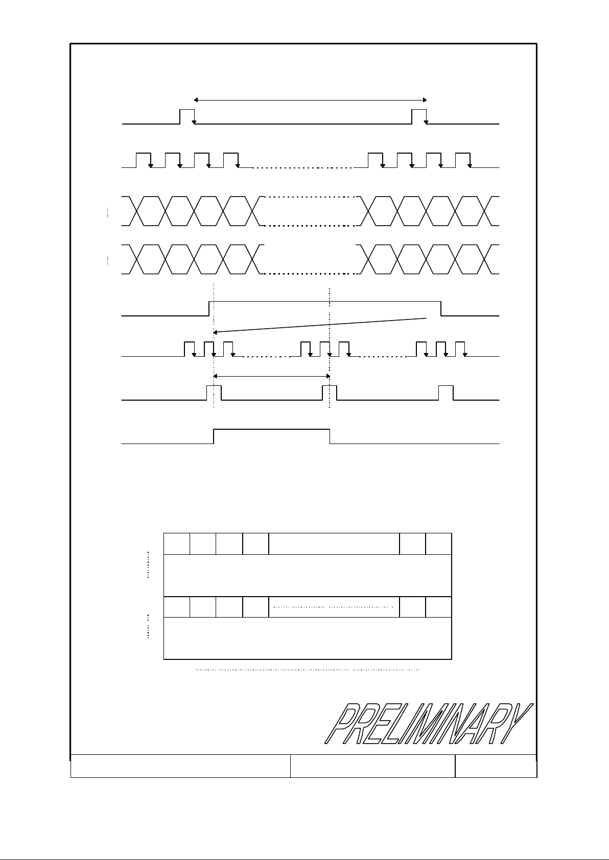
t
WDL
t
SD
t
r
t
f
t
DH
t
DS
t
WCKL
t
LH
t
SL
CP
t
LD
t
LS
LP
DISPOFF
DU0~DU3
DL0~DL3
t
WLPH
TOP DATALAST DATA
t
WCK
t
WCKH
FLM
t
SU
t
H
F-51430NFU-FW-AA (AA) No. 2001-0115 OPTREX CORPORATION Page 6/20
2.4. Timing Chart
2.5. Comparison of Display and Data
T=0.0595ms typ.
240xT
FLM
(Reduction)
(Reduction)
LP
FLM
M
DU3
DU0
CP
LP
#1 DATA
SEGSEG SEGSEG SEGSEG SEGSEG
640636 84 640636 84
637~633~ 5~ 1~ 637~633~ 5~ 1~
DL3
DL0
#241 DATA
SEGSEG SEGSEG SEGSEG SEGSEG
12801276 648644 12801276 648644
1277~1273~
645~
641~ 1277~1273~ 645~
641~
SEG1 SEG640
#241
#1
#240
#480
DU2DU3
DU0~DU3
DL0~DL3
SEG641 SEG1280
DU0DU1
DU0
DU1
DL2DL3 DL0DL1 DL0DL1
UPPER DATA
LOWER DATA
 Loading...