

OPTREX F-51167NCU-FW-AA Datasheet
Approved by
Checked by
Checked by
Prepared by
LCD Module Specification
F-51167NCU-FW-AA
F-51167NCU-FW-AA
Type No.
F-51167NCU-FW-AAF-51167NCU-FW-AA
First Edition
Aug 9, 2000
Final Revision
********
Table of Contents
1. General Specifications............................................................................ 2
2. Electrical Specifications.......................................................................... 3
3. Optical Specifications............................................................................. 8
4. I/O Terminal.......................................................................................... 10
5. Test......................................................................................................... 12
6. Appearance Standards........................................................................... 13
7. Code System of Production Lot .........................................................15
8. Type Number ........................................................................................ 15
9. Applying Precautions............................................................................ 15
10. Precautions Relating Product Handling.............................................. 16
11. Warranty................................................................................................. 17
Rev. Date Page Comment
Revision History
Production Div.
Quality Assurance Div.
Design Engineering Div.
Production Div.
F-51167NCU-FW-AA (AA) No.2000-0249 OPTREX CORPORATION Page 1/17
OPTREX
1.General Specifications
Operating Temp.
Storage Temp.
Dot Pixels
Dot Size
Dot Pitch
Viewing Area
Outline Dimensions
W eight
LCD Type
Viewing Angle
Data Transfer
Duty
Backlight
Drawings
min. 0℃ ~ max. 50℃
:
min. -20℃ ~ max. 70℃
:
320×3 [R.G.B] (W) × 240 (H) dots
:
0.10 (W) × 0.34 (H) mm
:
0.12 (W) × 0.36 (H) mm
:
122.0 (W) × 92.0 (H) mm
:
*
:
167.1
(W) × 109.0 (H) × 8.0 max. ( D) mm
* Without CFL Cable
204g max.
:
CTD-17753
:
( F-STN / Color-mode / Transmissive )
12:00
:
8-bit parallel data transfer
:
1/240
:
Cold Cathode Fluorescent Lamp (CFL) × 1
:
Dimensional Outline UE-300830
:
F-51167NCU-FW-AA (AA) No.2000-0249 OPTREX CORPORATION Page 2/17
OPTREX
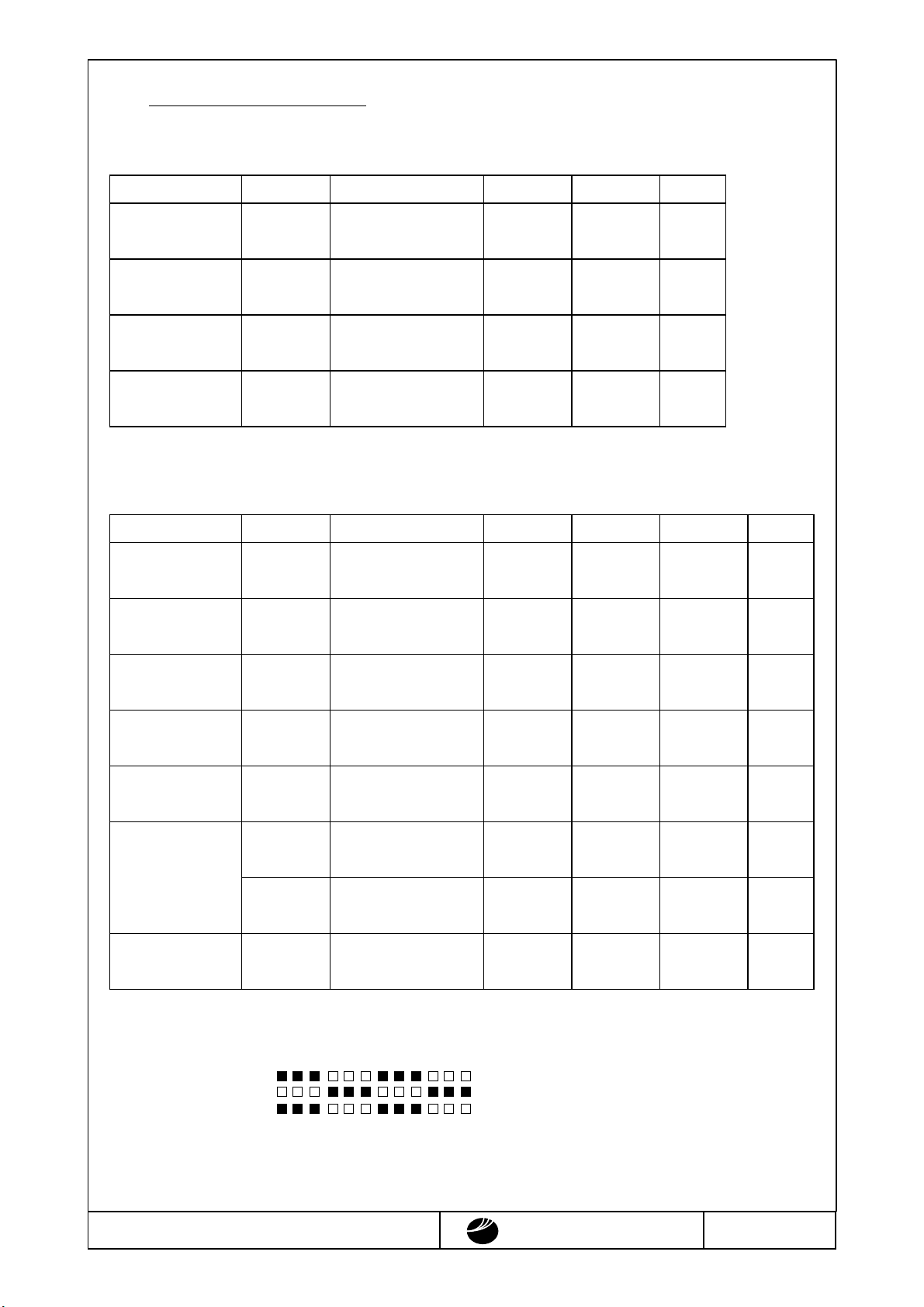
2.Electrical Specifications
2.1.Absolute Maximum Ratings
Parameter Symbol Conditions Min. Max. Units
V
=0V
SS
Supply Voltage
(Logic)
Supply Voltage
(LCD Drive)
Input Voltage VI
VADJ
Input Voltage
2.2.DC Characteristics
Parameter Symbol Conditions Min. Typ. Max. Units
Supply Voltage
(Logic)
Supply Voltage
(LCD Drive)
V
CC1-VSS
V
CC2-VSS
V
ADJ-VSS
V
CC1-VSS
V
CC2-VSS
-0.3 7.0 V
-
0 6.0 V
-
-0.3 V
-
0 3.0 V
-
3.0 - 5.5 V
-
3.0 - 5.5 V
-
+0.3 V
CC1
Ta=25℃, V
SS
=0V
Voltage for Contrast
V
ADJ-VSS
0.8 - 2.7 V
-
Adjustment (Note1)
High Level
VIH V
=3.0~5.5V 0.8× V
CC1
CC1
V
-
Input Voltage
Low Level
VIL V
=3.0~5.5V 0 - 0.2× V
CC1
Input Voltage
IV
CC1
V
CC1-VSS
=5.0V
20.0 40.0 mA
-
Supply Current
(Note2) IV
Clock Frequency
V
CC2
f
V
CP
CC2-VSS
=3.0~5.5V
CC1
=5.0V
40.0 60.0 mA
-
-
30 MHz
-
Duty=50%
Note1:The relation between Voltage for Contrast Adjustment and LCD Contrast is shown as follows;
0.8V(Bright)~2.7V(dark)
Note2:Supply current which checker pattern displayed.
GBR
GBRGBRGBR
f
V
F
=70Hz
OD
=26.6
V
CC1
V
CC1
F-51167NCU-FW-AA (AA) No.2000-0249 OPTREX CORPORATION Page 3/17
OPTREX
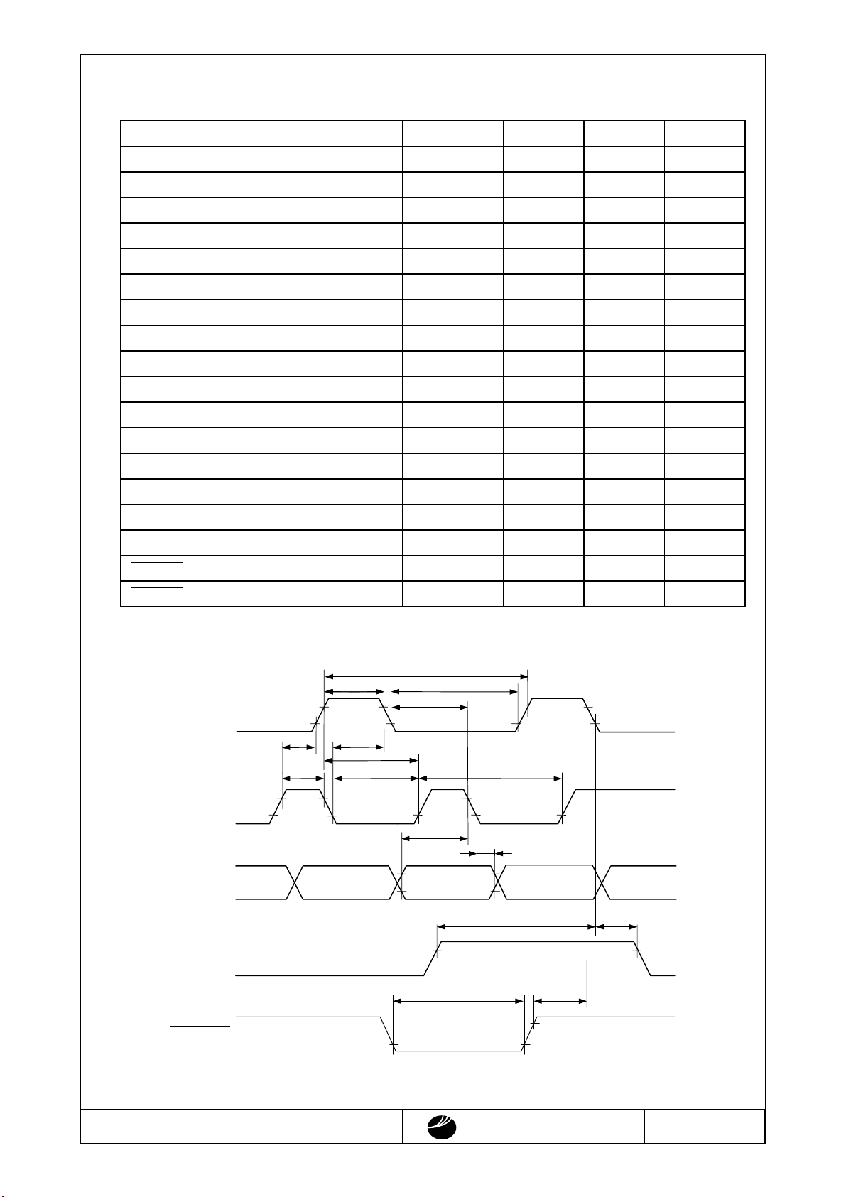
2.3. AC Characteristics
Parameter Symbol Min. Max. Units
=3.0~5.5V
V
CC1
LP Cycle Time
LP High Level Width
LP Low Level Width
Rise/Fall Time
FLM Setup Time
FLM Hold Time
CP Cycle Time
CP High Level Width
CP Low Level Width
LP Setup Time 1
LP Setup Time 2
LP Hold Time
Data Setup Time
Data Hold Time
LP ↑ to CP ↑
LP ↓ to CP ↓
DISPOFF Low Level Width
t
LP
t
WLH
t
WLL
t
t
Note 1 - 6.6 ns
r
d
,
t
st
t
hd
t
CP
t
WCH
t
WCL
t
st1
t
st2
t
hd1
t
st3
t
hd2
t
LH
t
LS
t
WDL
-
5 - ns
40 - ns
-
1000 - ns
-
60 - ns
-
30 - ns
-
40 - ns
-
15 - ns
-
15 - ns
-
30 - ns
-
30 - ns
-
15 - ns
-
15 - ns
-
15 - ns
-
25 - ns
-
25 - ns
-
100 - ns
-
DISPOFF Cancellation Time
t
SD
20 - ns
-
Note 1:The rise and fall times (tr, tf ) must satisfy the following relationships.
t
(
r, tf
1/f-2×
≦
t
)/2 f:
W
frequency
t
Minimum palse width
:
W
LP
LP
IH
V
IL
V
st2
t
t
CP
V
IL
V
WCH
IH
WLH
t
st1
t
LS
t
t
WCL
D0~D7
LAST DATA
V
V
t
WLL
t
LH
t
hd1
t
t
CP
st3
t
t
hd2
IH
IL
TOP DATA
ST
t
hd
t
IH
FLM
V
WDL
t
SD
t
DISPOFF
VIH=0.7×V
VIL=0.3×V
CC1
CC1
F-51167NCU-FW-AA (AA) No.2000-0249 OPTREX CORPORATION Page 4/17
OPTREX
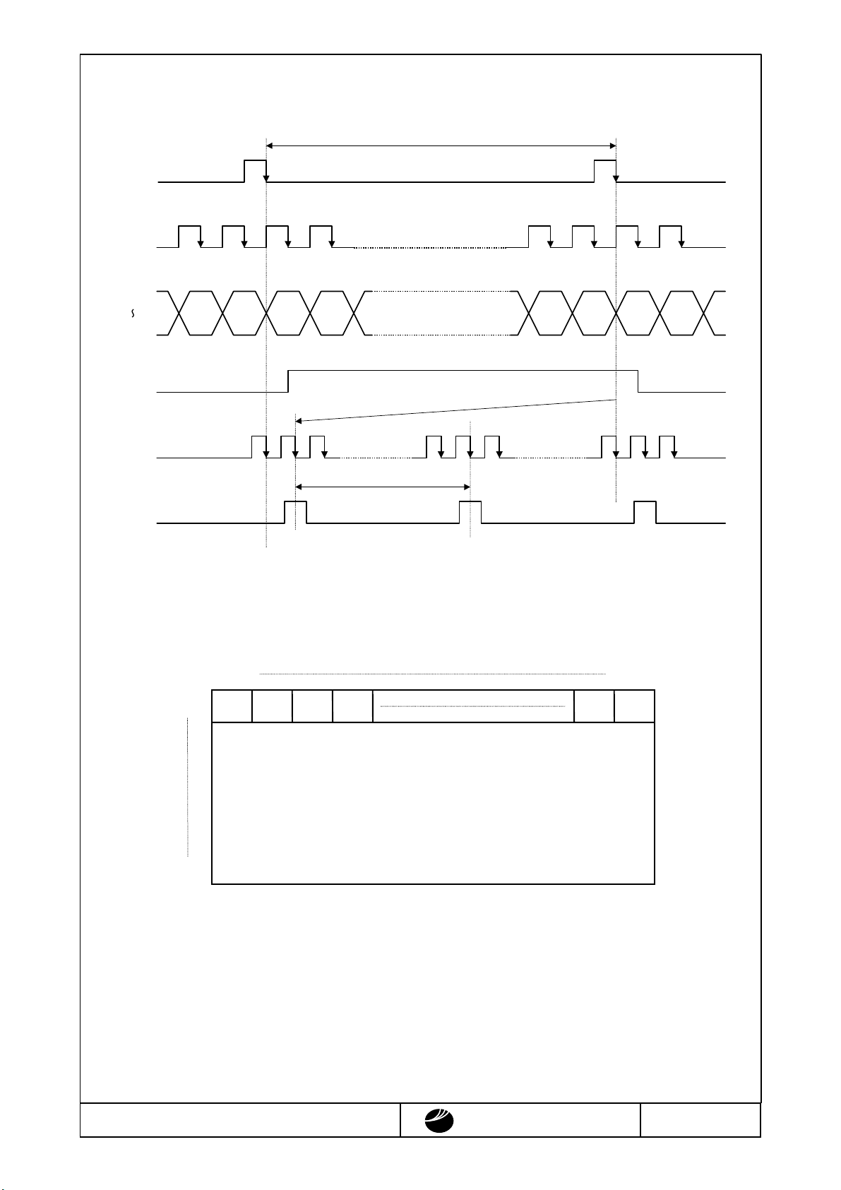
2.4.Timing Chart
T=0.0595ms typ.
LP
CP
D0
D7
~
945
SEGSEG SEGSEG SEGSEG SEGSEG
~
~
953
960952 168 960952 168
1
~
9
~
#1 DATA
945
~
953
~
~
1
9
~
FLM
LP
(Reduction)
240×T
FLM
(Reduction)
2.5.Comparison of Display and Data
SEG1 SEG960
#1
D7
D6
D4D5 D0D1
TOP VIEW
D0~D7
#240
F-51167NCU-FW-AA (AA) No.2000-0249 OPTREX CORPORATION Page 5/17
OPTREX
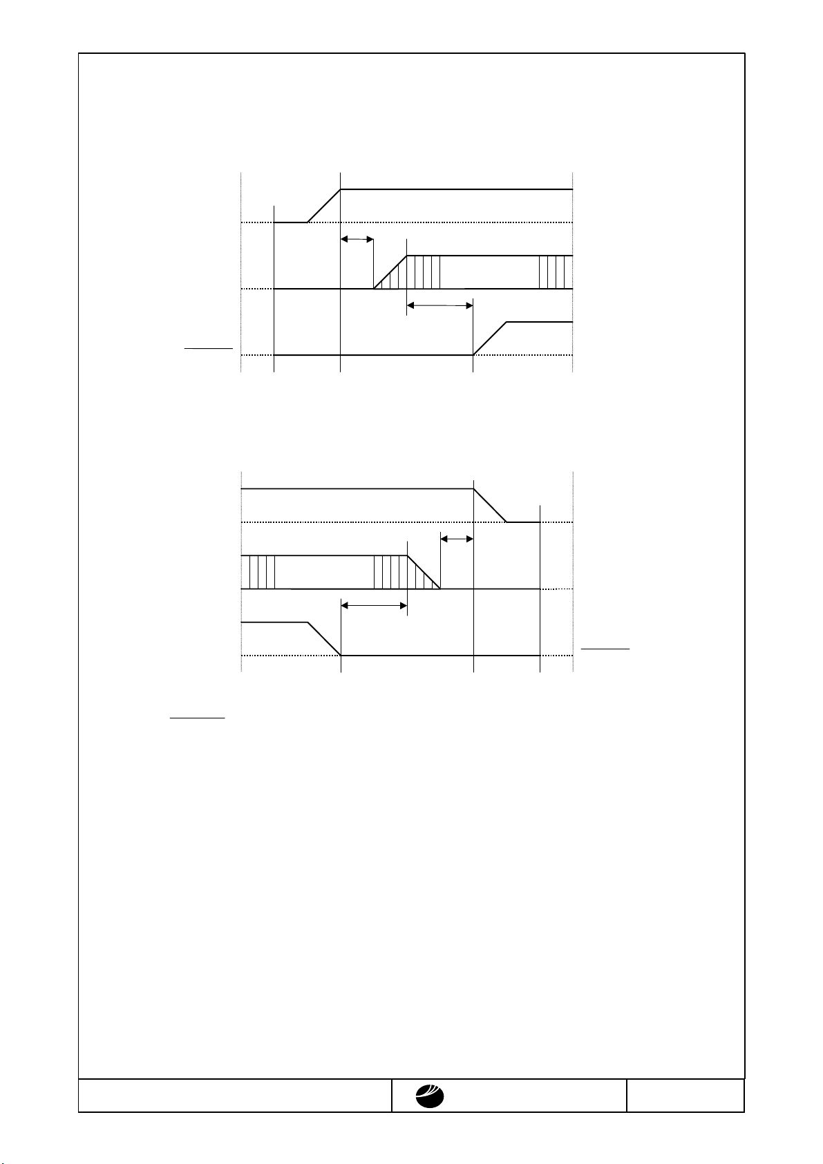
2.6.Power Supply ON/OFF Sequence
2.6.1.ON Sequence
SIGNAL
LEVEL
VCC1,VCC2
VCC1,VCC2
0≦t
VSS
SIGNAL
50 ms≦t
VCC1
VSS
VCC1
DISPOFF
VSS
2.6.2.OFF Sequence
LEVEL
SIGNAL
VCC1,VCC2
VSS
VCC1
0≦t
VCC1,VCC2
VSS
200 ms≦t
SIGNAL
VCC1
VSS
DISPOFF
Please maintain the above sequence when turning on and off the power supply of the module.
If DISPOFF is supplied to the module
hile internal alternate signal for LCD driving (M) is
w
unstable, DC component will be supplied to the LCD panel. This may cause damage the LCD
module.
F-51167NCU-FW-AA (AA) No.2000-0249 OPTREX CORPORATION Page 6/17
OPTREX
 Loading...