

OPTREX DMF6104NB-FW Datasheet
DMF6104NB-FW (AA) No.97-0138 OPTREX CORPORATION Page 1/17
OPTREX
Type No.
*******
June 2, 1997
First Edition
Final Revision
Quality Assurance Div.
Production Div.
Checked by
Checked by
Approved by
Production Div.
Design Engineering Div.
Prepared by
LCD Module Specification
DMF6104NB-FW
DMF6104NB-FWDMF6104NB-FW
DMF6104NB-FW
Table of Contents
1. General Specifications.............................................................................2
2. Electrical Specifications...........................................................................3
3. Optical Specifications..............................................................................8
4. I/O Terminal...........................................................................................10
5. Test..........................................................................................................12
6. Appearance Standards............................................................................13
7. Code System of Production Lot..........................................................16
8. Type Number .........................................................................................16
9. Applying Precautions.............................................................................16
10. Handling Precautions.............................................................................17
Revision History
Rev. Date Page Comment
DMF6104NB-FW (AA) No.97-0138 OPTREX CORPORATION Page 2/17
OPTREX
1.General Specifications
Operating Temp.
:
min. 10℃ ~ max. 40℃
Storage Temp.
:
min. -20℃ ~ max. 60℃
Dot Pixels
:
256 (W) × 128 (H) dots
Dot Size
:
0.43 (W) × 0.43 (H) mm
Dot Pitch
:
0.47 (W) × 0.47 (H) mm
Viewing Area
:
127.0 (W) × 70.0 (H) mm
Outline Dimensions
:
167.0 (W) × 116.0 (H) × 24.0 (D) mm
W eight
:
250g max.
LCD Type
:
NSD-7451
( STN / Blue-mode / Transflective )
Viewing Angle
:
6:00
Data Transfer
:
4-bit parallel data transfer
Backlight
:
Cold Cathode Fluorescent Lamp (CFL) × 1
Drawings
:
Dimensional Outline UE-32050B

DMF6104NB-FW (AA) No.97-0138 OPTREX CORPORATION Page 3/17
OPTREX
2.Electrical Specifications
2.1.Absolute Maximum Ratings
V
SS
=0V
Parameter Symbol Conditions Min. Max. Units
Supply Voltage
(Logic)
VCC-VSS
-
-0.3 6.0 V
Supply Voltage
(LCD Drive)
VCC-VEE
-
0 30.0 V
Input Voltage VI
-
-0.3 VCC+0.3 V
2.2.DC Characteristics
Ta=25℃, V
SS
=0V
Parameter Symbol Conditions Min. Typ. Max. Units
Supply Voltage
(Logic)
VCC-VSS
-
4.5 - 5.5 V
Supply Voltage
(LCD Drive)
VCC-VEE Shown in 3.1 V
High Level
Input Voltage
VIH VCC=5.0V±10% 0.8×VCC
-
V
CC
V
Low Level
Input Voltage
VIL VCC=5.0V±10% 0 - 0.2×VCC V
High Level
Output Voltage
VOH IOH=-0.2mA VCC-0.4
-
V
CC
V
Low Level
Output Voltage
VOL IOL=0.2mA 0 - 0.4 V
Supply Current
ICC VCC-VSS=5.0V
-
5.0 20.0 mA
I
EE
VCC-VEE=13.8V
-
4.7 15.0 mA
DMF6104NB-FW (AA) No.97-0138 OPTREX CORPORATION Page 4/17
OPTREX
2.3.AC Characteristics
V
CC
=5.0V±10%
Parameter Symbol Min. Max. Units
Clock Pulse Width
t
WC
100 - ns
Latch Pulse High Level Width
t
WL
125 - ns
Clock Pulse Rise/Fall Time
t
r, tf
-
50 ns
CP→LP Rise Time
t
CL
63 - ns
CP→LP Fall Time
t
LSU2
90 - ns
LP→CP Rise Time
t
LSU1
90 - ns
LP→CP Fall Time
t
LC
63 - ns
Data Setup Time
t
DSU
50 - ns
Data Hold Time
t
DHD
80 - ns
FLM Data Setup Time
t
SETUP
100 - ns
FLM Data Hold Time
t
HOLD
100 - ns
t
HOLD
t
SETUP
t
r
t
f
t
DHD
t
DSU
t
WC
t
LC
t
LSU2
CP
t
CL
t
LSU1
LP
FLM
D0~D3
t
WL
t
WC
DMF6104NB-FW (AA) No.97-0138 OPTREX CORPORATION Page 5/17
OPTREX
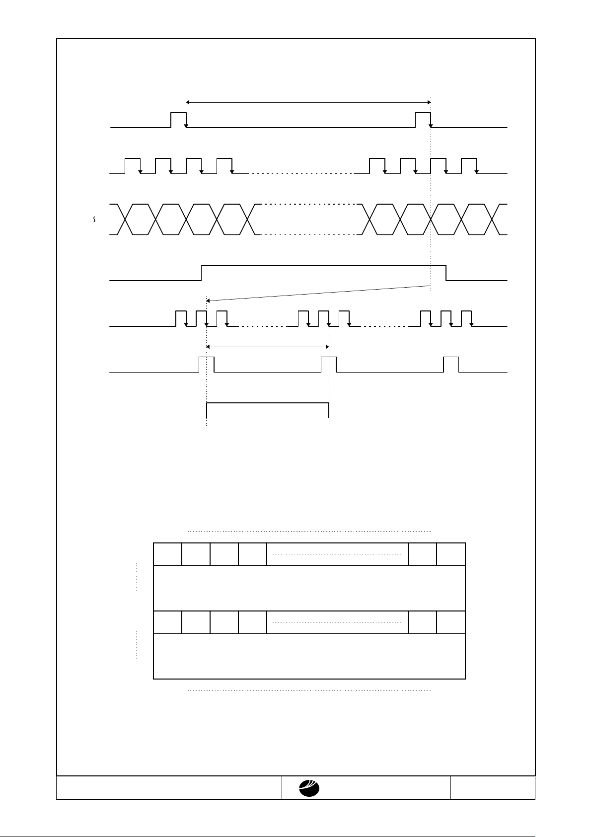
2.4.Timing Chart
2.5.Comparison of Display and Data
T=0.223ms typ.
64×T
FLM
(Reduction)
(Reduction)
LP
FLM
M
D3
D0
CP
LP
~
#1 + #65 DATA
SEGSEG SEGSEG SEGSEG SEGSEG
512508 84512508 84
509
~
505
~
5
~
1
~
509
~
505
~
5
~
1
~
SEG1 SEG256
#65
#1
#64
#128
D2D3
D0~D3
D0~D3
SEG257 SEG512
D0D1 D0D1
D2D3 D0D1 D0D1
DMF6104NB-FW (AA) No.97-0138 OPTREX CORPORATION Page 6/17
OPTREX
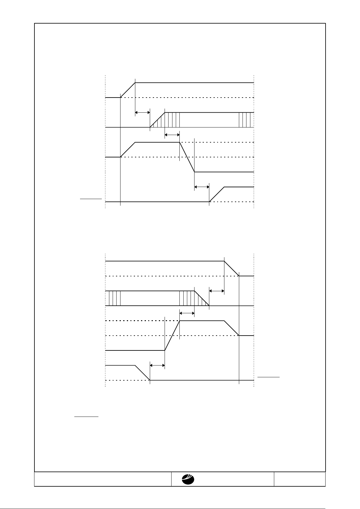
2.6.Power Supply ON/OFF Sequence
2.6.1.ON Sequence
2.6.2.OFF Sequence
Please maintain the above sequence when turning on and off the power supply of the module.
If DISPOFF is supplied to the module
w
hile alternate signal for LCD driving (M) is unstable,
DC component will be supplied to the LCD panel. This may cause damage the LCD module.
VCC
VSS
VEE
VSS
VSS
VCC
VSS
VCC
DISPOFF
VEE
VCC
0≦t
0≦t
SIGNAL
SIGNAL
LEVEL
VCC
0≦t
VCC
VSS
VEE
VSS
VSS
VCC
VSS
VCC
DISPOFF
VEE
VCC
0≦t
0≦t
SIGNAL
SIGNAL
LEVEL
VCC
0≦t
 Loading...