

OPTEK OP224ESA-B1, OP224ESA-B3, OP224SCC-B3, OP224SCC-C1, OP224SCC-C3 Datasheet
...
Fea tures
• Processed to Optek’s Military
screening program patterned after
ESA/SCC Generic Specification No.
5000
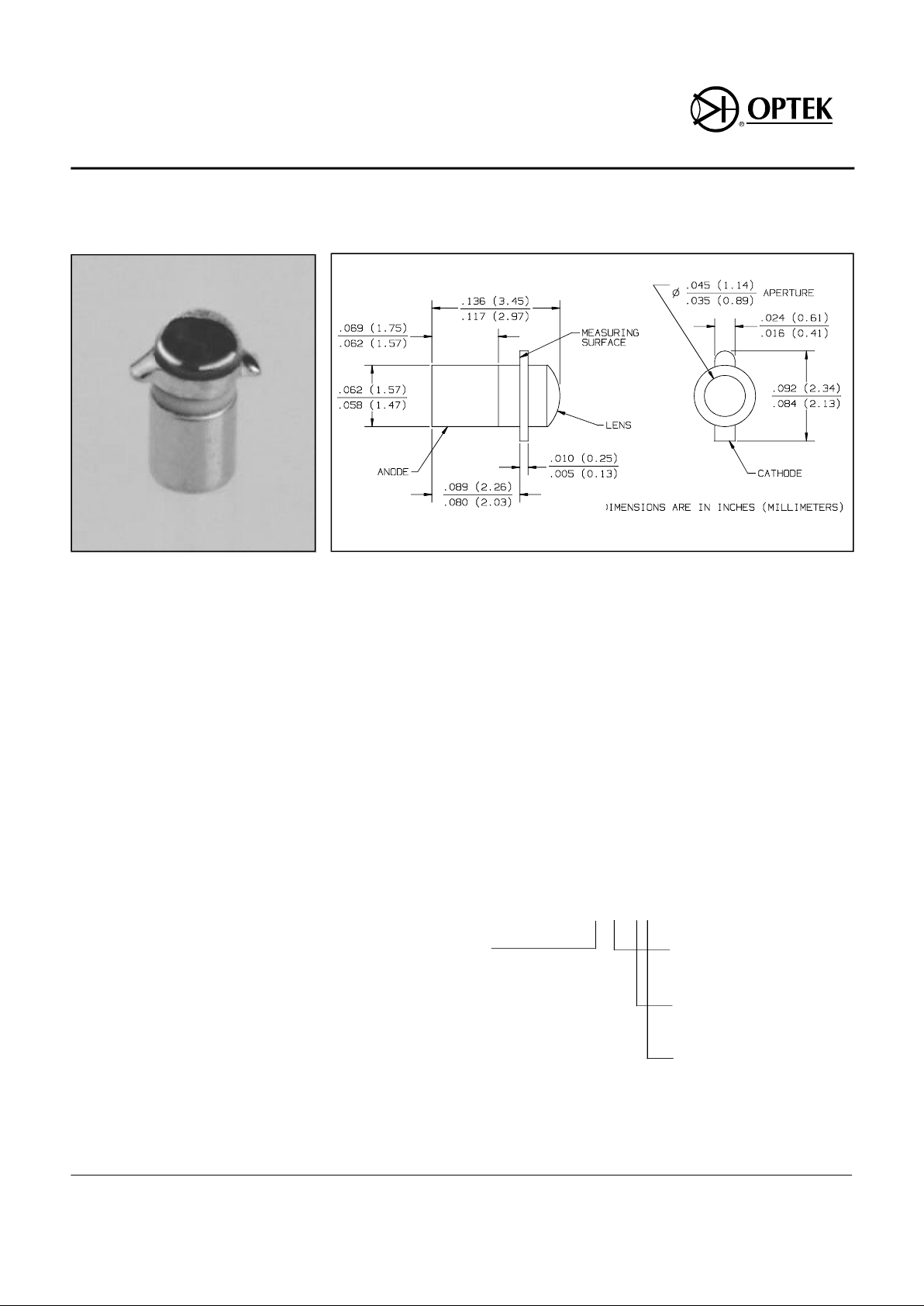
• Miniature hermetically sealed “pill”
package
• Twice the power output of GaAs at the
same drive current
• Mechanically and spectrally matched
to the OP600 series phototransistor
De scrip tion
The OP224ESA is a high reliability
gallium aluminum arsenide infrared
emitting diode mounted in miniature “pill”
type hermetically sealed package. This
package style is intended for direct
mounting into PC boards.
All devices are processed to Optek’s 100
percent screening program patterned
after ESA/SCC Generic Specification No.
5000. See page 13-4 for details.
Gallium aluminum arsenide features
twice the radiated output of gallium
arsenide at the same forward current.
With a wavelength centered at 890
nanometers, it closely matches the
spectral response of silicon
phototransistors, such as Optek’s OP600
high reliability series.
Ab so lute Maxi mum Rat ings (TA = 25o C un less oth er wise noted)
Stor age Tem pera ture Range . . . . . . . . . . . . . . . . . . . . . . . . . . . . . -65o C to +150o C
Op er at ing Tem pera ture Range. . . . . . . . . . . . . . . . . . . . . . . . . . . . -55o C to +125o C
Sol der ing Tem pera ture (for 5 sec. with sol der ing iron). . . . . . . . . . . . . . . . . 240o C
(1)
Re verse Volt age . . . . . . . . . . . . . . . . . . . . . . . . . . . . . . . . . . . . . . . . . . . . . . . . . 2.0 V
Con tinu ous Fow ard Cur rent . . . . . . . . . . . . . . . . . . . . . . . . . . . . . . . . . . . . . . . 100 mA
Power Dis si pa tion. . . . . . . . . . . . . . . . . . . . . . . . . . . . . . . . . . . . . . . . . . . . 100 mW
(2)
Notes:
(1) No-clean or low solids, RMA flux is recommended. Duration can be extended to 10 seconds
max. when flow soldering.
(2) Derate linearly 1.00 mW/o C above 25o C.
(3) X defines the Testing Level per ESA/SCC 5000 Generic Specification Chart III. X will be
either “B” (full processing) or “C” (reduced processing).
N defines Lot Acceptance Tests per ESA/SCC Generic Specification 5000 Chart V. N will be
either 1, 2, or 3. See Generic Processing Table for details.
Prod uct Bul le tin OP224ESA
Sep tem ber 1996
High Re li abil ity GaA lAs In fra red Emit ting Di ode
Type OP224ESA- XN
(3)
Op tek Tech nol ogy, Inc. 1215 W. Crosby Road Car roll ton, Texas 75006 (972) 323- 2200 Fax (972) 323- 2396
Part Num ber Guide
OP224ESA- XN
Op tek
High Re li abil ity
Part Num ber
ESA/SCC Speci fi ca tion
No. 5000
“B” - Full Proc ess ing
“C” - Re duced Proc ess ing
Level ”1” En vi ron men tal/Me chani cal plus Level
2 & 3
Level “2” Life Test ing
plus Level 3
Level “3" Elec tri cal In spec tion
13-26
Type OP224ESA-XN
Op tek re serves the right to make changes at any time in or der to im prove de sign and to sup ply the best pos si ble prod uct.
Op tek Tech nol ogy, Inc. 1215 W. Crosby Road Car roll ton, Texas 75006 (972) 323- 2200 Fax (972) 323- 2396
Elec tri cal Char ac ter is tics (TA = 25o C un less oth er wise noted)
Sym bol Pa rame ter Min Typ Max Units Test Con di tions
I
R
Reverse Current (High Temperature)
100
µA
VR = 2 V, TA = 125o C
I
R
Reverse Current (Low Temperature)
10
µA
VR = 2 V, TA = -55o C
P
O
Radiant Power Output 1.50 mW IF = 50 mA
V
F
Forward Voltage 0.80 1.80 V IF = 50 mA
I
R
Reverse Current
100
µA
VR = 2.0 V
λp
Wavelength at Peak Emission
850 910 nm
IF = 50 mA
B Spectral Bandwidth Between Half Power Points 80 nm IF = 50 mA
∆λp/∆T
Spectral Shift with Temperature
0.18 nm/oC
IF = Constant
θ
HP
Emission Angle at Half Power Points
18 Deg.
IF = 50 mA
V
F
Forward Voltage (High Temperature) 0.70 1.70 V IF = 50 mA, TA = 100o C
V
F
Forward Voltage (Low Temperature) 1.20 2.00 V IF = 50 mA, TA = -55o C
E
e(APT)
Apertured Radiant Incidence 3.50 mW/cm2IF = 50 mA
(6)
I
e
Radiant Intensity 5.64 mw/Sr IF = 50 mA
(6)(7)
tr, t
f
Rise and Fall Time
800 ns
IF = 50 mA, PW = 10 µS, dc = 10%
(4) Vis ual in spec tion based upon Op tek’s in ter pre ta tion of pre- cap in spec tion as speci fied in MIL- S- 19500/548 as ap pli ca ble for LED’s.
(5) E
e(APT)
is meas ured us ing a 0.031 inches (0.78 mm) di ame ter ap er tured sen sor placed 0.50 inches (12.7 mm) from the mount ing plane.
(6) Ie is cal cu lated from the meas ured value of E
e(APT)
as sum ing the source to be lo cated at the mount ing plane. The con ver sion for this ap er ture
and dis tance is Ie(mW/Sr) = E
e(APT)
(mW/cm2) x 1.61.
13-27
 Loading...