

Page 1
EVBUM2704
VE-Tract Dual EZ Kit
Quickstart Guide
This document is intended to be a guide to explain the
connectivity and usage of the evaluation kit described in the
table below. The evaluation kit is designed to quickly
perform benchmarking or product evaluation at specific
operating conditions in a lab environment. The product
should only be operated and handled by qualified personnel
with sufficient electrical engineering training and
experience.
Applies to the following parts.
Table 1.
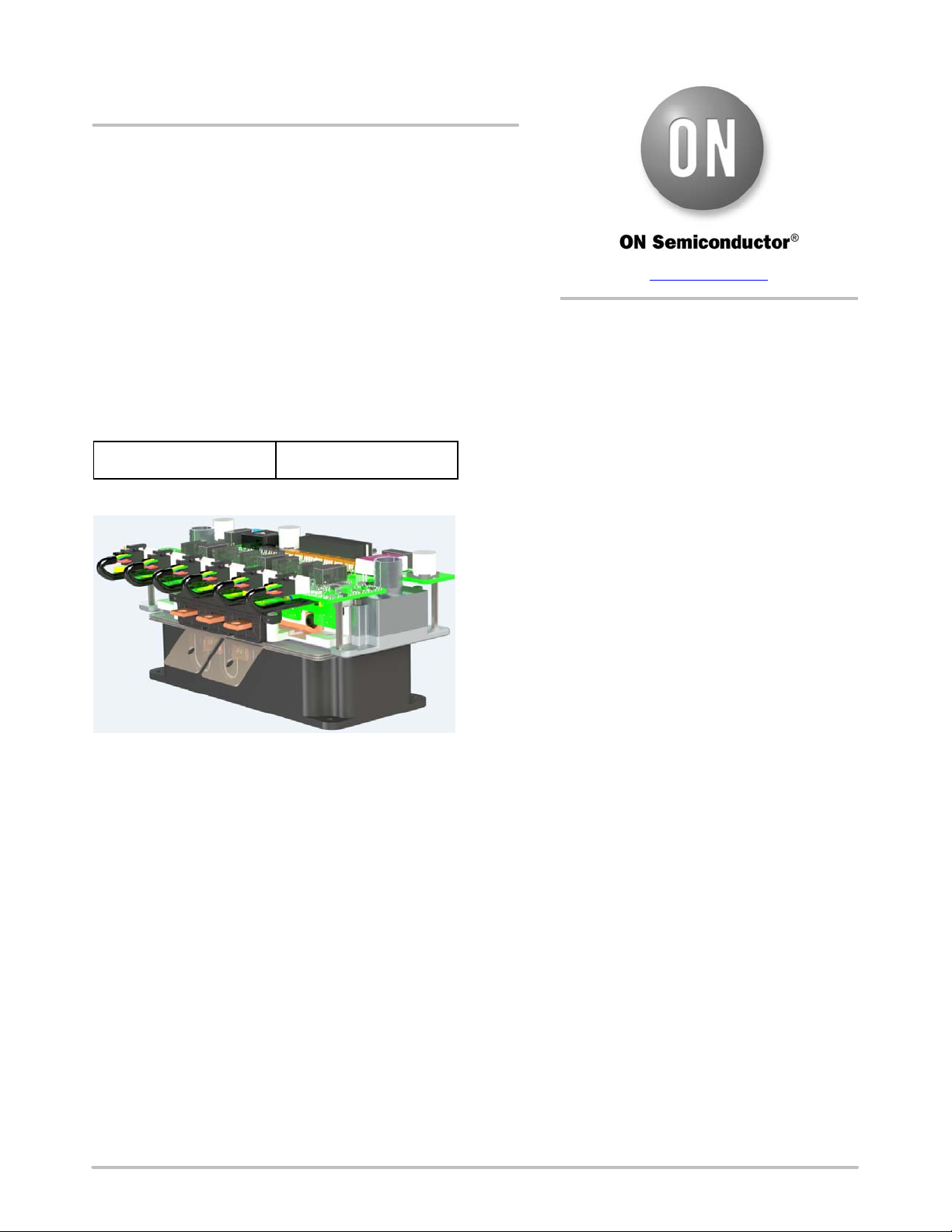
NVG800A75L4DSC−EVK 750 V, 800 A based 3−ph
Evaluation kit
Figure 1. NVG800A75L4DSC−EVK
INTRODUCTION
The VE−Trac Dual Evaluation Kit consists of three
VE−Trac Dual power modules (NVG800A75L4DSC)
mounted on dual side cooling heatsink, with a 6−ch Gate
driver board, DC Link capacitor and external hall−effect
current sense feedback for motor control. The kit does not
include a PWM controller. The user must user their on PWM
controller to operate the system. The evaluation kit allows
the customers to evaluate VE−Trac Dual power module
performances in their early stage of inverter development.
The kit can be used as a double pulse tester to measure key
switching parameters or used as a 3−ph inverter for motor
control.
www.onsemi.com
EVAL BOARD USER’S MANUAL
VE−Trac Dual evaluation kit features:
• Inverter evaluation Hardware kit for EV/HEV Traction
Inverter applications (up to 150 kW)
• VE−Trac Dual NVG800A75L4DSC with 800 A, 750 V
Field stop 4 IGBT/Diode chipset
• Automotive Isolated high current and high efficiency
IGBT gate driver with internal galvanic isolation,
NCD57000
• Implementation of Faster and simpler OCP enabled by
On−Chip Current Sensing feature in the power modules
• Implementation of faster and closer to true Tvj OTP with
integrated to On−Chip Temperature Sensing feature in the
power modules
• Custom designed dual side cooler offers low pressure
drop with excellent thermal performance
• Custom Film DC Link capacitor rated up to 500 VDC,
500 mF.
TECHNICAL DETAILS
ON Semiconductor’s latest generation of IGBTs and
Diodes are incorporated into the VE−Trac Dual products.
The 750 V products use the latest 4
IGBTs from ON Semiconductor.
Block Diagram
In this section, we describe the evaluation kit in detail,
including block diagram, operating conditions, key
components, On−chip current/temperature sensing and
protection features.
th
Generation of FS4
© Semiconductor Components Industries, LLC, 2019
July, 2020 − Rev. 1
1 Publication Order Number:
EVBUM2704/D
Page 2
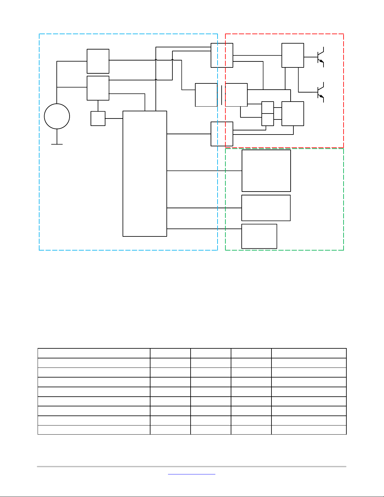
EVBUM2704
Vin
GNDC
Boost
Based on
NCV8870
20 V
Buck
Based on
NCV890100
3.3 V
LDO
1.8 V
Logic
Block
CPLD
5M40ZE64C5N
NCD57000
Flyback NCP 1031
Optical
isolator
15
GND
−9
LDOs
OUTPUTS
Master Fault OC
Temp Fault OC
Over Curr fault OC
Ready OC
HV_fault OC
INPUTS
6x PWM diff
FOD8071
Reset
Halt
ANALOG OUT
Input Voltage
T° IGBT
LEM
Push−Pull
Driver
−5
+5
Sensing
circuit
x3
Q1
Q2
Figure 2. Simplified Block Diagram
The simplified block diagram gives a quick overview of
the evaluation kit. The dotted lines show the different
isolated sections of the system.
exposed high voltage and high temperatures that when
accidentally contacted can result in electrical shock or
severe burns. Therefore, it should only be handled by
professionals with sufficient electrical engineering training
Maximum Ratings
The VE−Trac Dual Evaluation kit is intended to be
operated in a lab testing environment and should not be
regarded as a protected system. Parts of the design have
Table 2. SUMMARY OF OPERATING CONDITIONS
Parameter Symbol Min Max Conditions
Gate Driver Board Control Power V
DC Link Voltage V
Peak Collector Phase Current (1 ms) I
Maximum IGBT/FWD Junction Temperature T
Wait time after short circuit SC 1 s −
PCB Temperature T
Switching frequency F
Coolant Temperature T
Driv
BUS
CPEAK
VJ_Max
PCB
SW
c
and experience. Moreover, the operating conditions
especially the thermal limits described below should be
followed strictly.
9 V 15 V
0 V 500 V Limited by Capacitor
−1600 A 1600 A Limited by Tvj_Max
−40°C 175°C
− 85°C
− 12 kHz
−40°C 65°C
www.onsemi.com
2
Page 3
EVBUM2704
Key Components
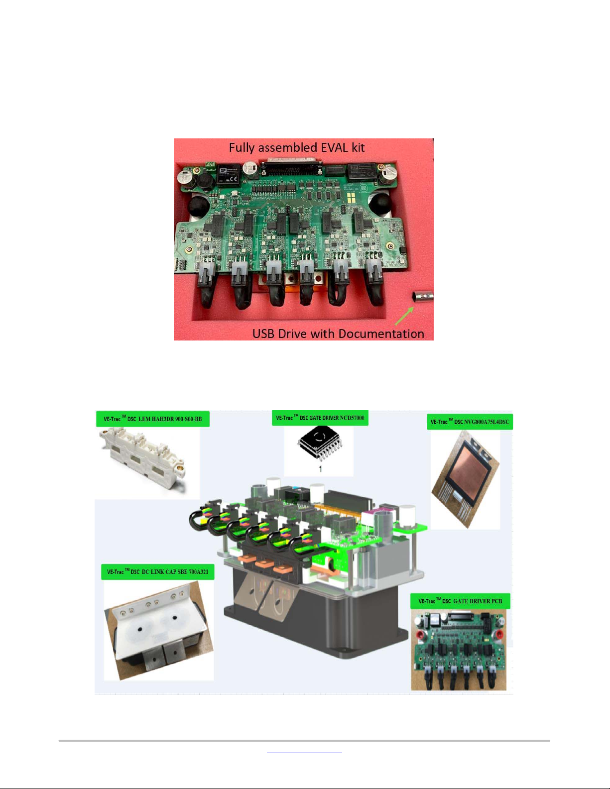
The evaluation kit is shipped in a hard plastic case with the
following contents:
n Full assembled evaluation kit hardware
n USB Drive containing all the required documentation
Figure 3. Shipping Contents in Case
The assembled evaluation kit assembly itself consists of
the following major components.
Figure 4. Major Components that Make Up the Evaluation Kit
www.onsemi.com
3
Page 4
EVBUM2704
Table 3. SUPPLIERS FOR THE MAJOR COMPONENTS OF THE EVALUATION HARDWARE
Part Number Manufacturer Description
NVG800A75L4DSC with reference
heatsink stack
NCD57000 ON Semiconductor Automotive Isolated Gate Driver
Dual side cooler ON Semiconductor ON Semi design with outsourced manufacturing.
700A321 SBE
HAH3DR 900−S00−BB LEM Hall Current Transducer. ±900 A
On−chip Current Sensing and Temperature Sensing
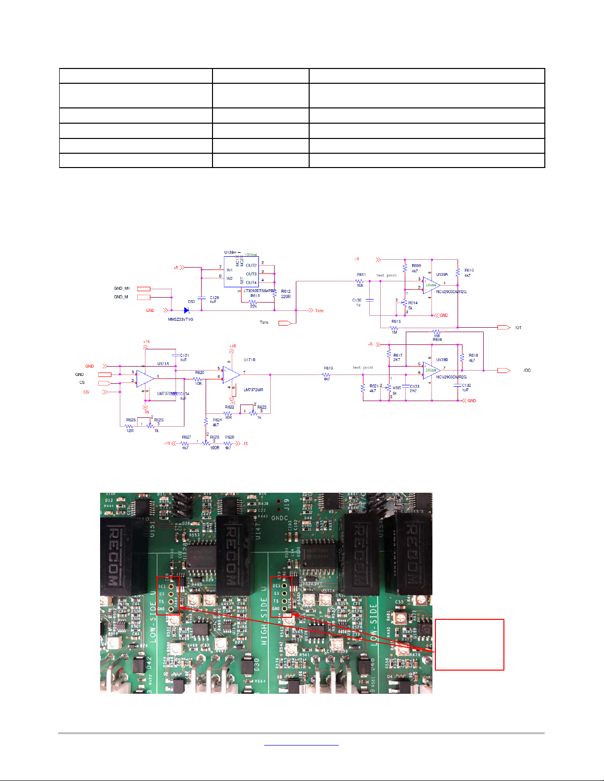
One of the kay advantage of the VE−Trac Dual power
modules is the integrated On−chip current sensing and
On−chip temperature sensing. The Evaluation kit offers
users the option of monitoring the junction temperature and
ON Semiconductor Automotive VE−Trac Dual power module with FS4 750 V 800 A
IGBT and Diode
DC Link Capacitor 500 V, 500 mF
current of all six IGBTs in real time. OCP/OTP protections
is implemented using the on−chip sensors. Below
schematics show how On−chip current sensing is
implemented as well as test points for verification purpose.
Figure 5. Schematics of Implementing On−chip Current Sensing
Figure 6. Test Points for On−chip Current and Temperature Sense
www.onsemi.com
4
Test points for
current/temp
sense, of which
all 6 switches
are available
Page 5
EVBUM2704
Protection Features
Over Current Protection (OCP) and Over Temperature
Protection (OTP) are implemented by sensing the On−chip
current sensor and On−chip temperature sensor respectively.
Besides this, the traditional desaturation protection is also
implemented to allow users to compare it with the On−chip
current sense protection. The protection trigger levels are set
as below:
• Over Current Protection (OCP) for all phases set to
1600 A
Table 4. FAULT INDICATION LED MATRIX
OCP_FAULT_
Phases
Phase_U_HS D12 D10 D28
Phase_U_LS D13 D11 D40
Phase_V_HS D16 D14 D61
Phase_V_LS D17 D15 D64
Phase_W_HS D20 D18 D34
Phase_W_LS D21 D19 D54
LED
• Over Temperature Protection (OTP) for all phases set to
150°C
• DC Link Over Voltage Fault Threshold set to 550 VDC
NOTE: All faults are the latching type and requires a
reset to clear the fault latch to start operating
again. During a fault incident, a LED is lit to
help the user to identify the cause of the fault.
Below is Fault Indication LED Matrix for the
VE−Trac Dual evaluation kit. Normal operation
indication LEDs are off when fault occurs, refer
to Figure 11 for locations of fault LEDs
DRVER_
OTP_FAULT_LED
FAULT_LED
PCBs AND CONNECTORS
There is a total of five (5) PCBs in the evaluation kit
assembly.
1. Power Module interface boards (3)
2. Gate driver board (1)
3. Current sensor board (1)
Power Module Interface boards are not accessible to the
user and is soldered to the signal pins of each of the three
VE−Trac Dual modules. An interface cable with a signal
connector extends from the interface boards to connect to
the gate driver board. The purpose this arrangement is to
make it easy to remove the driver board for replacement or
for trouble shooting purpose.
Gate driver board is the main PCB with several
connectors on it. It interfaces with the user’s Motor Control
Unit (MCU), the hall−effect current sensors, Power modules
and aux. power input.
www.onsemi.com
5
Page 6

EVBUM2704
Table 5. CONNECTOR X1:
Pin# Signal Function Specification
1 POWER_VSS Aux. Power RTN Ground return for External Power Input
2 POWER_VSS Aux. Power RTN Ground return for External Power Input
3 LEM_PHASE_W Analog Output 0 – 10 V LEM Phase W output
4 GND_I/O Ground reference Ground reference for LEM PCB
5 READY Digital I/O 3.3 − 5 V Gate driver ready status
6 GND_RDY Ground reference Ground reference for driver ready status
7 OC I/O_FLT Digital I/O 3.3 V − 5 V Digital output Over Current Fault
8 GND_FLT Ground reference Ground reference for Digital outputs
9 MASTER_FAULT Digital I/O 3.3 V − 5 V Digital output Driver Fault
10 +15_I/O1 Power supply Power supply for LEM PCB
11 HALT_CMD Digital I/O 0 − 3.3 V OR 5V Digital input
12 GND_I/O1 Ground reference Ground reference for LEM PCB
13 PWM_IN−_U_H Digital I/O 0 − 3.3 V OR 5 V PWM Logic input
14 PWM_IN+_U_H Digital I/O 0 − 3.3 V OR 5 V PWM Logic input
15 PWM_IN−_V_H Digital I/O 0 − 3.3 V OR 5 V PWM Logic input
16 PWM_IN+_V_H Digital I/O 0 − 3.3 V OR 5 V PWM Logic input
17 PWM_IN−_W_H Digital I/O 0 − 3.3 V OR 5 V PWM Logic input
18 PWM_IN+_W_H Digital I/O 0 − 3.3 V OR 5 V PWM Logic input
19 CGND1 Ground reference Ground reference for digital logic.
20 POWER_VDD Aux. Power IN 9 V to 15 V External Power input
21 POWER_VDD Aux. Power IN 9 V to 15 V External Power input
22 LEM_PHASE_U Analog Output 0 – 10 V LEM Phase U output
23 LEM_PHASE_V Analog Output 0 – 10 V LEM Phase V output
24 RES I/O Digital I/O 0 − 3.3 V OR 5 V external reset input
25 GND RES_I/O Ground reference Ground reference for Reset / Halt−Cmd
26 HV_FAULT_I/O Digital I/O 3.3 V − 5 V Digital output HVDC Fault
27 GND_I/O2 Ground reference Ground reference for DC_LINK+/W_I/O
28 W_I/O Analog Output 0 – 10 V Phase W Temp Sensing
29 DC_LINK+ Analog Output 0 – 10 V DC BUS Voltage Sensing
30 T I/O_FAULT Digital I/O 3.3 V − 5 V Digital output over Temp Fault
31 GND_I/O2 Ground reference Ground reference for DC_LINK+/W_I/O
32 PWM_IN−_U_L Digital I/O 0 − 3.3 V OR 5 V PWM Logic input
33 PWM_IN+_U_L Digital I/O 0 − 3.3 V OR 5 V PWM Logic input
34 PWM_IN−_V_L Digital I/O 0 − 3.3 V OR 5 V PWM Logic input
35 PWM_IN+_V_L Digital I/O 0 − 3.3 V OR 5 V PWM Logic input
36 PWM_IN−_W_L Digital I/O 0 − 3.3 V OR 5 V PWM Logic input
37 PWM_IN+_W_L Digital I/O 0 − 3.3 V OR 5 V PWM Logic input
Table 6. CONNECTOR J18
Pin# Signal Function Specification
1 POWER_VDD Aux. Power IN 9 – 15 VDC, 4 A
2 POWER_VSS Aux. Power RTN GND return for Aux. power
www.onsemi.com
6
Page 7

EVBUM2704
Table 7. CONNECTOR LEM1
Pin# Signal Function Specification
1 +15VI/O Power +15 V Power supply for Isolated Signal
2 GND_I/O Ground Ground return for +15 VI/O
3 IU Sensor output LEM Phase U output
4 IV Sensor output LEM Phase V output
5 IW Sensor output LEM Phase W output
6 GND_I/O Ground Ground return for +15 VI/O
Table 8. CONNECTOR J11/J12/J13
Pin# Signal Function Specification
1 FLT−H Protection Gate Driver fault High Side
2 FLT−L Protection Gate Driver fault Low Side
3 OTS_HS Protection Over Temperature High Side
4 OTS_LS Protection Over Temperature Low Side
5 OCS_HS Protection Over Current High Side
6 OCS_LS Protection Over Current Low Side
7 IN+_H PWM Logic PWM Logic High Side
8 IN+_L PWM Logic PWM Logic Low Side
Table 9. CONNECTOR J16
Pin# Signal Function Specification
1 IW Signal LEM Sensor Phase W output
2 NC − −
3 IV Signal LEM Sensor Phase V output
4 NC − −
5 IU Signal LEM Sensor Phase U output
6 NC − −
7 TEMP_IGBTW_I/O Analog output Phase W Low side temperature sensor output
8 GND_I/O Ground Ground return for +15 VI/O
Current Sensor Board conditions the feedback signals
from the hall−effect sensors and interfaces with the gate
driver board via a flat ribbon cable.
Table 10. CONNECTOR J2
Pin# Signal Function Specification
1 +15VI/O Power +15 V Power supply for Isolated Signal
2 GND_I/O Ground Ground return for +15 VI/O
3 IU Sensor output LEM Phase U output
4 IV Sensor output LEM Phase V output
5 IW Sensor output LEM Phase W output
6 GND_I/O Ground Ground return for +15 VI/O
www.onsemi.com
7
Page 8

EVBUM2704
OPEN LOOP OPERATION
This section gives a quick start guide for operating
VE−Trac Dual evaluation kit in open loop operation and
provides a list of equipment needed.
Equipment for Evaluation of VE−Trac Dual Evaluation
Kit
• Power Supply: 9 V − 15 V, 4 A
• HVDC Power Supply: 0 − 500 V 40 A (depends on the
load)
• Load: Passive 3 ph Inductive load or AC Induction
Machine
• Scope: 4 channel digital scope
• HV Differential Probe: 1500 Vpk 200 MHz Bandwidth
• Current Probe: 6000 A 30 MHz Bandwidth
• DVM: General Digital Multi−meter
• MCU or DSP Eval Board: Open loop PWM control
algorithm software
• Cooling System : 50/50 Ethylene Glycol/Water Flow rate
8 − 10 LPM
• Hose: ¾” ID, 1” OD, rated to 100°C, 45 PSI @ 25°C
• Cooling System for Load: Liquid or Air−cooled.
Connections with Control Power and MCU/DSP
Interface
The evaluation kit requires an external MCU or DSP Eval
Board for PWM control signals for open loop operation. The
interface features a standard DB−37 connector. Below
figure and table show the pin out definitions.
Figure 7. Controller Interface
www.onsemi.com
8
Page 9
EVBUM2704
Table 11. CONTROLLER INTERFACE SIGNAL USED
Pin# Signal Function Specification
1 Vss Ground To be connected to ground
2 Vss Ground To be connected to ground
13 PWM_IN−_U_H PWM signal Differential pairs
14 PWM_IN+_U_H PWM signal Differential pairs
15 PWM_IN−_V_H PWM signal Differential pairs
16 PWM_IN+_V_H PWM signal Differential pairs
17 PWM_IN−_W_H PWM signal Differential pairs
18 PWM_IN+_W_H PWM signal Differential pairs
32 PWM_IN−_U_L PWM signal Differential pairs
33 PWM_IN+_U_L PWM signal Differential pairs
34 PWM_IN−_V_L PWM signal Differential pairs
35 PWM_IN+_V_L PWM signal Differential pairs
36 PWM_IN−_W_L PWM signal Differential pairs
37 PWM_IN+_W_L PWM signal Differential pairs
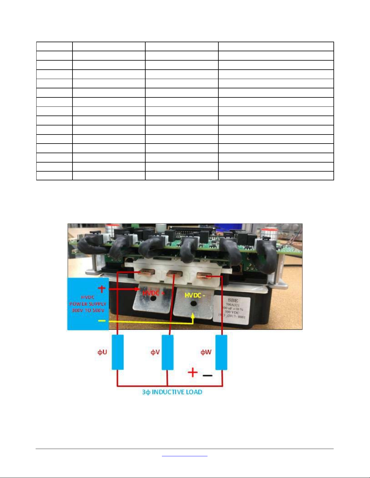
VE−Trac DSC Drive Connection for HVDC and LOAD
Figure 8 shows the right connection of HVDC power
supply and loads. Make sure a good electrical contact
between the power tabs to avoid generating excessive heat.
We recommend monitor the temperature of the power
terminals during operation and take corrective actions when
they are overheated.
Figure 8. Power and Load Connection
VE−Trac Dual Evaluation Kit Cooling System
The cooler can be connected with a ¾ inch Inside
Dimension and 1inch Outside Dimension flexible hose
interface. Use 50% Water/50% Ethylene Glycol as cooling
www.onsemi.com
fluid and make sure that cooling fluid corrosion protection
is compatible with aluminum heatsink. We strongly
recommend not use pure water as cooling fluid because it
might damage the heatsink.
9
Page 10

EVBUM2704
Figure 9. Cooling Interface Appearance
Figure 10. Example with Hose Interface Connected
Run the VE−Trac Dual Evaluation Kit in Open Loop
Configuration
Following are the steps to run the inverter in open loop
operation.
• Turn off all the power supplies
• Connect control power supply to Inverter at connector
J18, refer to Figure 7
• Connect logic PWM signal from DSP/MCU to gate driver
board at DB37 pin connector as shown in Figure 7
• Connect voltage/current probes to signals of interest, for
example PWM signal, phase current, IGBT collector
voltage etc.
• Connect DVM to monitor the IGBT virtual junction
temperature to the test points as shown in Figure 6
• Power on the DSP/MCU Board
• Connect USB from DSP/MCU Board to Host computer
for commanding the PWM signals duty ratio and Inverter
fundamental output frequency to the Inverter
• Set the control power supply as the following
♦ Voltage: 12 V
♦ Current Limit = 3 A
• Turn on the control power supply and all the fault LEDs
will be lit. Press the reset switch (see Figure 11) to clear
all the faults.
• Set the HVDC Power Supply to 400 V
• Turn on the HVDC Power supply
• Set the cooler system flow rate to desired value. eg
10 LPM to the power module.
• Turn on the cooling system to the Power module
• Turn on the cooling system to the Load
• Enable the Inverter by turning on the PWM Logic via host
computer
• Adjust the Duty ratio and Inverter fundamental frequency
to get desired output current
• Monitor the IGBT Junction Temperature
• Record the Cooler System Inlet and Outlet Temperature
• Record the output phase current
www.onsemi.com
10
Page 11

EVBUM2704
Figure 11. Location of Reset Switch
TEST RESULT SUMMARY
Following the steps listed above, inverter testing has been
done to verify the function of the evaluation kit as well as the
performance of the VE−Trac Dual power module. Driving
capability of the power module with reference cooling
140
120
100
80
TJ [°C]
60
40
20
0
0 100 200 300 400 500 600
heatsink was verified by monitoring On−chip temperature
sensor vs Phase current.
Test Results under the Condition of: Tcoolant = 25C
DC BUS = 400 V Fsw = 8 kHz / 10 kHz.
Flow rate = 10 LPM
TJ_8 kHZ [°C]
TJ_10 kHZ [°C]
I∅ [ARMS]
Figure 12. IGBT Junction Temperature vs Phase Current; Tcoolant = 25C Flow Rate = 10 LPM,
Bus Voltage = 400 V, Switching Freq = 8 & 10 kHz
www.onsemi.com
11
Page 12

EVBUM2704
Figure 13. Switching Waveforms, C1: U Phase Current; C2: W Phase Voltage (Low Side Switch);
C3: W Phase Current; C4: Input PWM Signal (W Phase Low Side)
Test Results under the Condition of: Tcoolant = 65 C
DC BUS = 400 V Fsw = 8 kHz / 10 kHz.
Flow rate = 10 LPM
180
160
140
120
TJ [°C]
100
TJ_8 kHZ [°C]
80
60
0 100 200 300 400 500 600
I∅ [ARMS]
TJ_10 kHZ [°C]
Figure 14. IGBT Junction Temperature vs Phase Current; Tcoolant = 65C Flow Rate = 10 LPM,
Bus Voltage = 400 V, Switching Freq = 8 kHz / 10 kHz
www.onsemi.com
12
Page 13

EVBUM2704
Figure 15. Switching Waveforms, C1: U Phase Current; C3: W Phase Current
VE−Trac is trademark of Semiconductor Components Industries, LLC (SCILLC) or its subsidiaries in the United States and/or other countries.
www.onsemi.com
13
Page 14

ON Semiconductor and the ON Semiconductor logo are trademarks of Semiconductor Components Industries, LLC dba ON Semiconductor or its subsidiaries in the United States and/or
other countries. ON Semiconductor owns the rights to a number of patents, trademarks, copyrights, trade secrets, and other intellectual property. A listing of ON Semiconductor’s
product/patent coverage may be accessed at www.onsemi.com/site/pdf/Patent−Marking.pdf
subject to all applicable copyright laws and is not for resale in any manner.
The evaluation board/kit (research and development board/kit) (hereinafter the “board”) is not a finished product and is as such not available for sale to consumers. The board is only intended
for research, development, demonstration and evaluation purposes and should as such only be used in laboratory/development areas by persons with an engineering/technical training
and familiar with the risks associated with handling electrical/mechanical components, systems and subsystems. This person assumes full responsibility/liability for proper and safe handling.
Any other use, resale or redistribution for any other purpose is strictly prohibited.
The board is delivered “AS IS” and without warranty of any kind including, but not limited to, that the board is production−worthy, that the functions contained in the board will meet your
requirements, or that the operation of the board will be uninterrupted or error free. ON Semiconductor expressly disclaims all warranties, express, implied or otherwise, including without
limitation, warranties of fitness for a particular purpose and non−infringement of intellectual property rights.
ON Semiconductor reserves the right to make changes without further notice to any board.
You are responsible for determining whether the board will be suitable for your intended use or application or will achieve your intended results. Prior to using or distributing any systems
that have been evaluated, designed or tested using the board, you agree to test and validate your design to confirm the functionality for your application. Any technical, applications or design
information or advice, quality characterization, reliability data or other services provided by ON Semiconductor shall not constitute any representation or warranty by ON Semiconductor,
and no additional obligations or liabilities shall arise from ON Semiconductor having provided such information or services.
The boards are not designed, intended, or authorized for use in life support systems, or any FDA Class 3 medical devices or medical devices with a similar or equivalent classification in
a foreign jurisdiction, or any devices intended for implantation in the human body. Should you purchase or use the board for any such unintended or unauthorized application, you shall
indemnify and hold ON Semiconductor and its officers, employees, subsidiaries, affiliates, and distributors harmless against all claims, costs, damages, and expenses, and reasonable
attorney fees arising out of, directly or indirectly, any claim of personal injury or death associated with such unintended or unauthorized use, even if such claim alleges that ON Semiconductor
was negligent regarding the design or manufacture of the board.
This evaluation board/kit does not fall within the scope of the European Union directives regarding electromagnetic compatibility, restricted substances (RoHS), recycling (WEEE), FCC,
CE or UL, and may not meet the technical requirements of these or other related directives.
FCC WARNING – This evaluation board/kit is intended for use for engineering development, demonstration, or evaluation purposes only and is not considered by ON Semiconductor to
be a finished end product fit for general consumer use. It may generate, use, or radiate radio frequency energy and has not been tested for compliance with the limits of computing devices
pursuant to part 15 of FCC rules, which are designed to provide reasonable protection against radio frequency interference. Operation of this equipment may cause interference with radio
communications, in which case the user shall be responsible, at its expense, to take whatever measures may be required to correct this interference.
ON Semiconductor does not convey any license under its patent rights nor the rights of others.
LIMITATIONS OF LIABILITY: ON Semiconductor shall not be liable for any special, consequential, incidental, indirect or punitive damages, including, but not limited to the costs of
requalification, delay, loss of profits or goodwill, arising out of or in connection with the board, even if ON Semiconductor is advised of the possibility of such damages. In no event shall
ON Semiconductor’s aggregate liability from any obligation arising out of or in connection with the board, under any theory of liability, exceed the purchase price paid for the board, if any.
For more information and documentation, please visit www.onsemi.com
.
. ON Semiconductor is an Equal Opportunity/Affirmative Action Employer. This literature is
PUBLICATION ORDERING INFORMATION
LITERATURE FULFILLMENT:
Email Requests to: orderlit@onsemi.com
ON Semiconductor Website: www.onsemi.com
TECHNICAL SUPPORT
North American Technical Support:
Voice Mail: 1 800−282−9855 Toll Free USA/Canada
Phone: 011 421 33 790 2910
Europe, Middle East and Africa Technical Support:
Phone: 00421 33 790 2910
For additional information, please contact your local Sales Representative
◊
www.onsemi.com
1
 Loading...