

Page 1
MMQA Quad Common
Anode Series
Preferred Devices
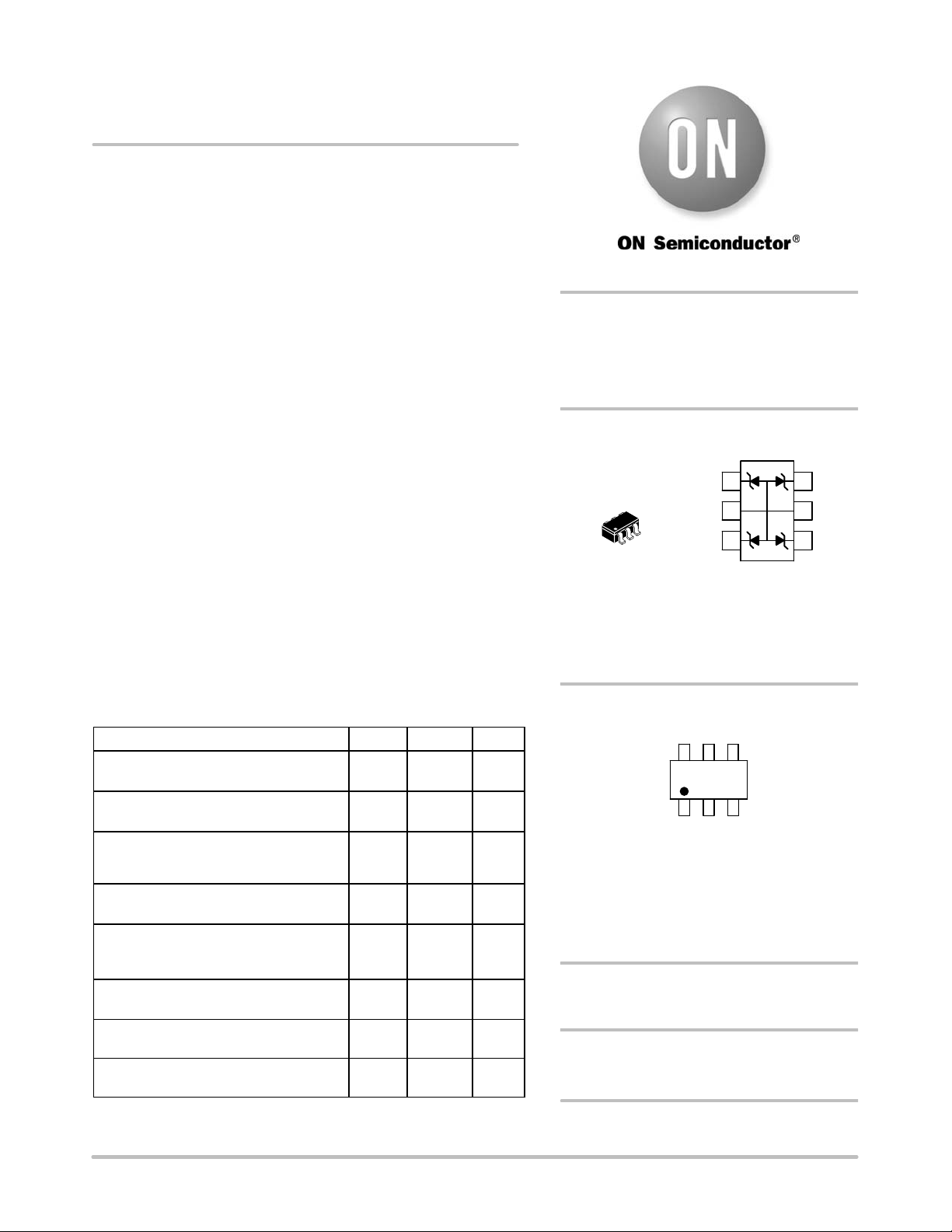
SC-74 Quad Monolithic
Common Anode
Transient Voltage Suppressors
for ESD Protection
http://onsemi.com
This quad monolithic silicon voltage suppressor is designed for
applications requiring transient overvoltage protection capability. It is
intended for use in voltage and ESD sensitive equipment such as
computers, printers, business machines, communication systems,
medical equipment, and other applications. Its quad junction common
anode design protects four separate lines using only one package.
These devices are ideal for situations where board space is at a
premium.
Features
•SC-74 Package Allows Four Separate Unidirectional Configurations
•Peak Power - Min. 24 W @ 1.0 ms (Unidirectional),
per Figure 5 Waveform
•Peak Power - Min. 150 W @ 20 ms (Unidirectional),
per Figure 6 Waveform
•Maximum Clamping Voltage @ Peak Pulse Current
•Low Leakage < 2.0 mA
•ESD Rating of Class N (exceeding 16 kV) per the Human Body Model
•Pb-Free Packages are Available
THERMAL CHARACTERISTICS (T
Characteristic Symbol Value Unit
Peak Power Dissipation @ 1.0 ms (Note 1)
@ TA ≤ 25°C
Peak Power Dissipation @ 20 ms (Note 2)
@ TA ≤ 25°C
Total Power Dissipation on FR‐5 Board
(Note 3) @ TA = 25°C
Thermal Resistance from
Junction-to-Ambient
Total Power Dissipation on Alumina
Substrate (Note 4) @ TA = 25°C
Derate above 25°C
Thermal Resistance from
Junction-to-Ambient
Junction and Storage Temperature Range TJ, T
Lead Solder Temperature - Maximum
(10 Second Duration)
= 25°C unless otherwise noted)
A
P
pk
P
pk
°PD° °225
R
q
JA
°PD° °300
R
q
JA
stg
T
L
24 W
150 W
1.8
556 °C/W
2.4
417 °C/W
°- 55 to
+150°
260 °C
mW°
mW/°C
°
mW°
mW/°C
°C
SC-74 QUAD TRANSIENT
VOLTAGE SUPPRESSOR
24 WATTS PEAK POWER
5.6 - 33 VOLTS
PIN ASSIGNMENT
1
2
6
1
SC-74
PLASTIC
CASE 318F
3
PIN 1. CATHODE
2. ANODE
3. CATHODE
4. CATHODE
5. ANODE
6. CATHODE
MARKING DIAGRAM
xxxMG
G
xxx = Device Code
M = Date Code*
G = Pb-Free Package
(Note: Microdot may be in either location)
*Date Code orientation may vary depending
upon manufacturing location.
DEVICE MARKING INFORMATION
See specific marking information in the device marking table
on page 5 of this data sheet.
ORDERING INFORMATION
See detailed ordering and shipping information in the table on
page 5 of this data sheet.
6
5
4
© Semiconductor Components Industries, LLC, 2007
July, 2007 - Rev. 7
Preferred devices are recommended choices for future use
and best overall value.
1 Publication Order Number:
MMQA/D
Page 2
MMQA Quad Common Anode Series
ELECTRICAL CHARACTERISTICS (T
= 25°C unless otherwise noted)
A
UNIDIRECTIONAL
(Circuit tied to pins 1, 2, and 5; Pins 2, 3, and 5; Pins 2, 4, and 5; or Pins 2, 5, and 6) (VF = 0.9 V Max @ IF = 10 mA)
Max
Reverse
Leakage
ZTIR
Current
V
R
Max Zener
Impedance
(Note 7)
ZZT @ IZT
(W) (mA)
Max
Reverse
Surge
Current
I
RSM
(A)
Device
Breakdown Voltage
V
ZT
(Note 5)
(V)
@ I
Min Nom Max (mA) (nA) (V)
MMQA5V6T1,T3 5.32 5.6 5.88 1.0 2000 3.0 400 3.0 8.0 1.26 - -
MMQA6V2T1,T3 5.89 6.2 6.51 1.0 700 4.0 300 2.66 9.0 10.6 - -
MMQA6V8T1,T3 6.46 6.8 7.14 1.0 500 4.3 300 2.45 9.8 10.9 100 250
MMQA12VT1,T3 11.4 12 12.6 1.0 75 9.1 80 1.39 17.3 14 - -
MMQA13VT1 12.4 13 13.7 1.0 75 9.8 80 1.29 18.6 15 - -
MMQA15VT1,T3 14.3 15 15.8 1.0 75 11 80 1.1 21.7 16 - -
MMQA18VT1,T3 17.1 18 18.9 1.0 75 14 80 0.923 26 19 - -
MMQA20VT1,T3 19 20 21 1.0 75 15 80 0.84 28.6 20.1 - -
MMQA21VT1,T3 20 21 22.1 1.0 75 16 80 0.792 30.3 21 - -
MMQA22VT1,T3 20.9 22 23.1 1.0 75 17 80 0.758 31.7 22 - -
MMQA24VT1,T3 22.8 24 25.2 1.0 75 18 100 0.694 34.6 25 - -
MMQA27VT1,T3 25.7 27 28.4 1.0 75 21 125 0.615 39 28 - -
MMQA33VT1,T3 31.4 33 34.7 1.0 75 25 200 0.504 48.6 37 - -
Max
Reverse
Voltage @
I
RSM
(Note 6)
(Clamping
Voltage)
V
RSM
(V)
Capacitance
@ 0 Volt
Maximum
Bias, 1 MHz
Temperature
Coefficient
of V
Z
(pF)
(mV/°C) Min Max
1. Non‐repetitive current pulse per Figure 5 and derate above TA = 25°C per Figure 4.
2. Non‐repetitive current pulse per Figure 6 and derate above TA = 25°C per Figure 4.
3. FR‐5 = 1.0 x 0.75 x 0.62 in.
4. Alumina = 0.4 x 0.3 x 0.024 in., 99.5% alumina
5. VZ measured at pulse test current IT at an ambient temperature of 25°C.
6. Surge current waveform per Figure 5 and derate per Figure 4.
7. ZZT is measured by dividing the AC voltage drop across the device by the AC current supplied. The specified limits are I
with AC frequency = 1 kHz.
TYPICAL CHARACTERISTICS
300
250
200
150
100
C, CAPACITANCE (pF)
50
0
5.6 6.8 12 20 27
VZ, NOMINAL ZENER VOLTAGE (V)
Figure 1. Typical Capacitance
BIASED AT 0 V
BIASED AT 1 V
BIASED AT 50%
OF VZ NOM
33
10,000
1,000
100
, LEAKAGE (nA)
R
I
10
0
5.6 6.8 20 27
VZ, NOMINAL ZENER VOLTAGE (V)
Figure 2. Typical Leakage Current
Z(AC)
= 0.1 I
+150°C
+25°C
-40°C
Z(DC)
33
,
http://onsemi.com
2
Page 3

MMQA Quad Common Anode Series
TYPICAL CHARACTERISTICS
300
250
ALUMINA SUBSTRATE
200
150
100
, POWER DISSIPATION (mW)
D
P
50
0
0 25 50 75 100 125 150 175
FR‐5 BOARD
TA, AMBIENT TEMPERATURE (°C)
Figure 3. Steady State Power Derating Curve
PULSE WIDTH (tP) IS DEFINED
t
r
100
VALUE (%)
50
PEAK VALUE-I
t
P
0
01234
RSM
HALF VALUE-
AS THAT POINT WHERE THE
PEAK CURRENT DECAYS TO 50%
OF I
.
RSM
tr ≤ 10 ms
I
RSM
2
t, TIME (ms)
Figure 5. 10 × 1000 ms Pulse Waveform
100
90
80
C
°
70
= 25
A
60
50
40
30
OR CURRENT @ T
20
10
0
PEAK PULSE DERATING IN % OF PEAK POWER
0 25 50 75 100 125 150 175 200
TA, AMBIENT TEMPERATURE (°C)
Figure 4. Pulse Derating Curve
100
t
r
90
80
70
60
50
40
30
20
% OF PEAK PULSE CURRENT
10
0
020406080
t
P
PEAK VALUE I
HALF VALUE I
@ 8 ms
RSM
PULSE WIDTH (tP) IS DEFINED
AS THAT POINT WHERE THE
PEAK CURRENT DECAY = 8 ms
/2 @ 20 ms
RSM
t, TIME (ms)
Figure 6. 8 × 20 ms Pulse Waveform
100
10
UNIDIRECTIONAL
Ppk PEAK SURGE POWER (W)
1.0
0.1 1.0 10 100 1000
PW, PULSE WIDTH (ms)
RECTANGULAR
WAVEFORM, TA = 25°C
Figure 7. Maximum Non-Repetitive Surge
Power, Ppk versus PW
Power is defined as V
x IZ(pk) where V
RSM
is the clamping voltage at IZ(pk).
http://onsemi.com
RSM
200
180
160
140
120
100
80
60
, PEAK SURGE POWER (W)
PK
40
P
20
0
10 × 100 WAVEFORM AS PER FIGURE 5
5.6 6.8 12 20 33
Figure 8. Typical Maximum Non-Repetitive
3
8 × 20 WAVEFORM AS PER FIGURE 6
NOMINAL V
Z
Surge Power, Ppk versus V
27
BR
Page 4

MMQA Quad Common Anode Series
N
G
D
TYPICAL COMMON ANODE APPLICATIONS
A quad junction common anode design in a SC-74
package protects four separate lines using only one package.
This adds flexibility and creativity to PCB design especially
Computer Interface Protection
KEYBOARD
TERMINAL
PRINTER
ETC.
I/O
Microprocessor Protection
when board space is at a premium. A simplified example of
MMQA Series Device applications is illustrated below.
A
B
FUNCTIONAL
C
DECODER
D
GND
MMQA SERIES DEVICE
MMQA SERIES DEVICE
ADDRESS BUS
I/O
RAM ROM
DATA BUS
CONTROL BUS
CPU
CLOCK
V
D
V
G
G
http://onsemi.com
4
Page 5

MMQA Quad Common Anode Series
DEVICE MARKING AND ORDERING INFORMATION
Device* Device Marking Package Shipping
MMQA5V6T1* 5A6 SC-74 3,000/Tape & Reel
MMQA6V2T1* 6A2 SC-74 3,000/Tape & Reel
MMQA6V2T3* 6A2 SC-74 10,000/Tape & Reel
MMQA6V8T1* 6A8 SC-74 3,000/Tape & Reel
MMQA12VT1* 12A SC-74 3,000/Tape & Reel
MMQA13VT1* 13A SC-74 3,000/Tape & Reel
MMQA15VT1* 15A SC-74 3,000/Tape & Reel
MMQA18VT1* 18A SC-74 3,000/Tape & Reel
MMQA20VT1* 20A SC-74 3,000/Tape & Reel
MMQA20VT3* 20A SC-74 10,000/Tape & Reel
MMQA21VT1* 21A SC-74 3,000/Tape & Reel
MMQA22VT1* 22A SC-74 3,000/Tape & Reel
MMQA24VT1* 24A SC-74 3,000/Tape & Reel
MMQA27VT1* 27A SC-74 3,000/Tape & Reel
MMQA27VT3* 27A SC-74 10,000/Tape & Reel
MMQA33VT1* 33A SC-74 3,000/Tape & Reel
†For information on tape and reel specifications, including part orientation and tape sizes, please refer to our Tape and Reel Packaging
Specifications Brochure, BRD8011/D.
*The “G'' suffix indicates Pb-Free package available.
†
Mechanical Characteristics:
Void‐free, transfer‐molded, thermosetting plastic case.
CASE:
FINISH: Corrosion resistant finish, easily solderable.
Package designed for optimal automated board assembly.
Small package size for high density applications.
Available in 8 mm Tape and Reel.
Use the Device Number to order the 7 inch/3,000 unit reel.
Replace the “T1” with “T3” in the Device Number to order the 13 inch/10,000 unit reel.
http://onsemi.com
5
Page 6

MMQA Quad Common Anode Series
PACKAGE DIMENSIONS
SC-74
CASE 318F-05
ISSUE M
0.05 (0.002)
D
H
E
1
23
456
E
b
e
A
A1
C
L
NOTES:
1. DIMENSIONING AND TOLERANCING PER ANSI Y14.5M, 1982.
2. CONTROLLING DIMENSION: INCH.
3. MAXIMUM LEAD THICKNESS INCLUDES LEAD FINISH
THICKNESS. MINIMUM LEAD THICKNESS IS THE MINIMUM
THICKNESS OF BASE MATERIAL.
4. 318F-01, -02, -03, -04 OBSOLETE. NEW STANDARD 318F-05.
DIMAMIN NOM MAX MIN
A1 0.01 0.06 0.10 0.001
b 0.25 0.37 0.50 0.010
c 0.10 0.18 0.26 0.004
D 2.90 3.00 3.10 0.114
E 1.30 1.50 1.70 0.051
q
e 0.85 0.95 1.05 0.034
L
H
E
q
STYLE 1:
PIN 1. CATHODE
MILLIMETERS
0.90 1.00 1.10 0.035
0.20 0.40 0.60 0.008
2.50 2.75 3.00 0.099 0.108 0.118
0° 10° 0° 10°
- -
2. ANODE
3. CATHODE
4. CATHODE
5. ANODE
6. CATHODE
INCHES
NOM MAX
0.039 0.043
0.002 0.004
0.015 0.020
0.007 0.010
0.118 0.122
0.059 0.067
0.037 0.041
0.016 0.024
SOLDERING FOOTPRINT*
2.4
0.094
0.95
1.9
0.074
0.7
0.028
0.037
0.95
0.037
1.0
0.039
SCALE 10:1
mm
ǒ
inches
Ǔ
*For additional information on our Pb-Free strategy and soldering
details, please download the ON Semiconductor Soldering and
Mounting Techniques Reference Manual, SOLDERRM/D.
ON Semiconductor and are registered trademarks of Semiconductor Components Industries, LLC (SCILLC). SCILLC reserves the right to make changes without further notice
to any products herein. SCILLC makes no warranty, representation or guarantee regarding the suitability of its products for any particular purpose, nor does SCILLC assume any liability
arising out of the application or use of any product or circuit, and specifically disclaims any and all liability, including without limitation special, consequential or incidental damages.
“Typical” parameters which may be provided in SCILLC data sheets and/or specifications can and do vary in different applications and actual performance may vary over time. All
operating parameters, including “Typicals” must be validated for each customer application by customer's technical experts. SCILLC does not convey any license under its patent rights
nor the rights of others. SCILLC products are not designed, intended, or authorized for use as components in systems intended for surgical implant into the body, or other applications
intended to support or sustain life, or for any other application in which the failure of the SCILLC product could create a situation where personal injury or death may occur. Should
Buyer purchase or use SCILLC products for any such unintended or unauthorized application, Buyer shall indemnify and hold SCILLC and its officers, employees, subsidiaries, affiliates,
and distributors harmless against all claims, costs, damages, and expenses, and reasonable attorney fees arising out of, directly or indirectly, any claim of personal injury or death
associated with such unintended or unauthorized use, even if such claim alleges that SCILLC was negligent regarding the design or manufacture of the part. SCILLC is an Equal
Opportunity/Affirmative Action Employer. This literature is subject to all applicable copyright laws and is not for resale in any manner.
PUBLICATION ORDERING INFORMATION
LITERATURE FULFILLMENT:
Literature Distribution Center for ON Semiconductor
P.O. Box 5163, Denver, Colorado 80217 USA
Phone: 303-675-2175 or 800-344-3860 Toll Free USA/Canada
Fax: 303-675-2176 or 800-344-3867 Toll Free USA/Canada
Email: orderlit@onsemi.com
N. American Technical Support: 800-282-9855 Toll Free
USA/Canada
Europe, Middle East and Africa Technical Support:
Phone: 421 33 790 2910
Japan Customer Focus Center
Phone: 81-3-5773-3850
http://onsemi.com
ON Semiconductor Website: www.onsemi.com
Order Literature: http://www.onsemi.com/orderlit
For additional information, please contact your local
Sales Representative
MMQA/D
6
 Loading...