

Page 1
SC-601
Speech And Music Processor
Data sheet
© 2002 Sensory Inc.
P/N 80-0207-A
1
Features
Advanced, integrated speech synthesizer for
high-quality sound.
Operates up to 12.32 MHz (Performs up to 12
MIPS)
Single chip solution for up to 24 Minutes of
speech (using 1.57 Mb of onboard program +
data ROM)
Supports high-quality synthesis algorithms
Such as MX, CX, Simple CX, LX, ADPCM, and
Polyphonic Music
Simultaneous speech plus music capabilities
Very low-power operation, ideal for handheld
devices
Low-voltage operation, sustainable by three
batteries
Reduced power stand-by modes, less than 10
µA in deep-sleep mode
640-Word RAM
32 I/O Pins consisting of: 24 general purpose
bit configurable I/O, 8 inputs with programmable
pullup resistor and a dedicated interrupt (KeyScan)
Direct Speaker Driver, 32Ω (PDM)
One-bit comparator with edge-detection
interrupt service
Resistor-trimmed oscillator or 32.768kHz crystal
reference oscillator
Serial scan port for in-circuit emulation and
diagnostics
The SC-601 is sold in die form or 100-pin LQFP
package.
An emulator device is available in a ceramic
package for development (SC-614-P).
Description
The SC-601 is a low-cost, mixed-signal
processor that combines a speech synthesizer,
general-I/O, onboard ROM, and direct speaker
drive in a single package. The computational
unit utilizes a powerful DSP which gives the SC601 unprecedented speed and computational
flexibility compared with previous devices of its
type. The SC-601 supports a variety of speech
and audio coding algorithms, providing range of
options for speech duration and sound quality.
The device consists of a micro-DSP core,
embedded program, and data memory, and a
self-contained generation system. Generalpurpose periphery is comprised of 32 bits of partially configurable I/O.
The core processor is a general-purpose 16-bit microcontroller with DSP capability. The basic core includes
computational unit (CU), data address unit, program address unit, two timers, eight level interrupt processor,
and several system and control registers. The core processor gives the SC-601 break-capability in emulation.
The processor is Harvard type for efficient DSP algorithm execution. It requires separate program and memory
blocks to permit simultaneous access. The ROM has a protection scheme to prevent third-party pirating. It is
configured in 32K 17-bit words.
The total ROM space is divided into three areas:
1. The lower 2K words are reserved by Sensory a built-in self-test
2. The upper 30K words are for user program/data
3. An additional 1 Mb data ROM provides for up to 24 minutes of speech.
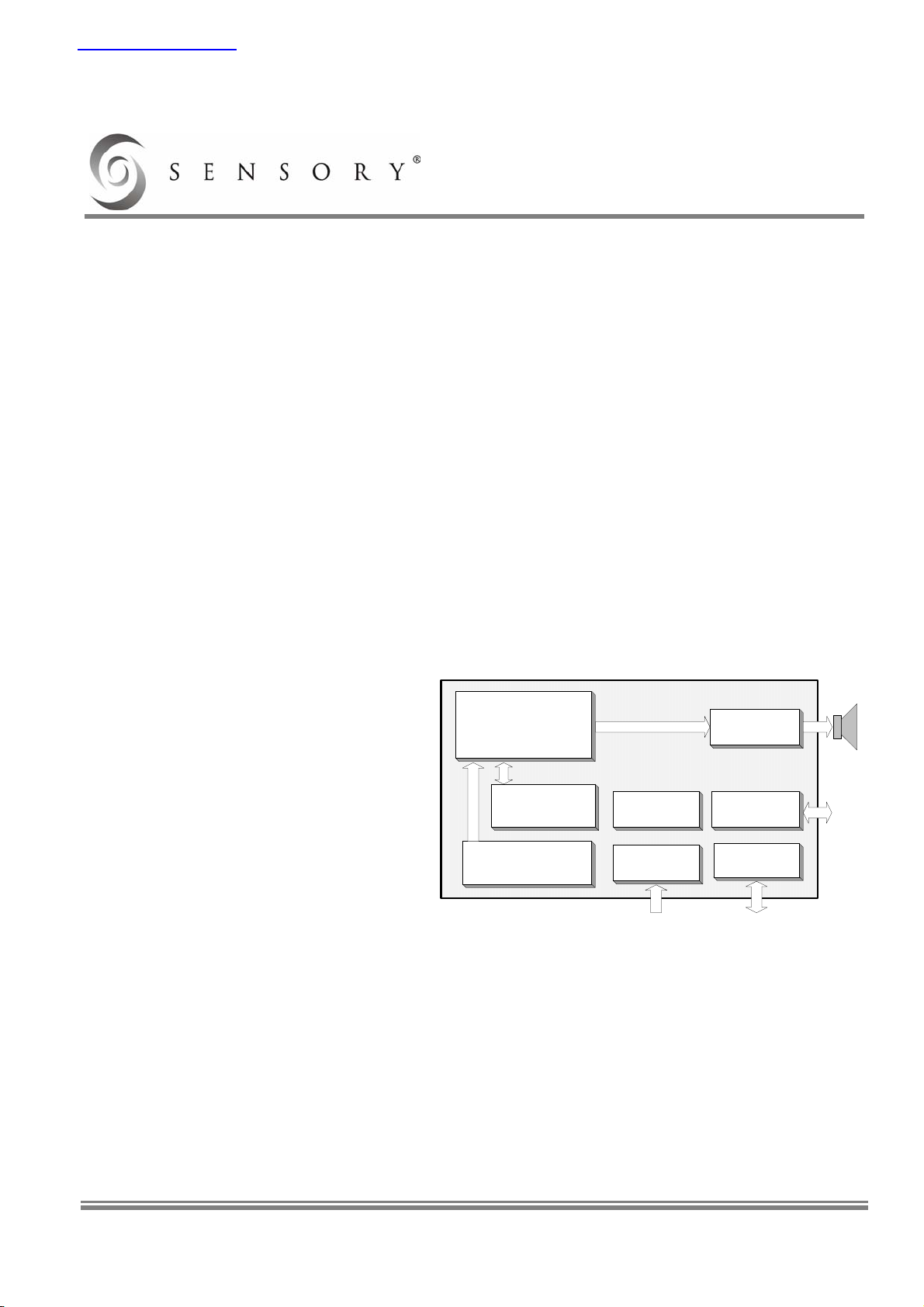
SC-601 Block Diagram
16-Bit
Microprocessor
640-words
RAM
192 KBytes
ROM
TIMER 1
TIMER 2
PLLM
10-Bit
DAC
32 I/O
COMPARATOR
查询SC601-R供应商
Page 2
SC-601
Data sheet
2
P/N 80-0207-A
© 2002 Sensory Inc.
The data memory is internal static RAM. The RAM is configured in 640 17-bit words. All memories are designed
to consume minimum power at a given system clock and algorithm acquisition frequency.
A flexible clock generation system enables the software to control the clock over a wide frequency range. The
implementation uses a phase-locked loop (PLL) circuit that drives the processor clock at a selectable frequency
between the minimum and maximum achievable. Selectable frequencies for the processor clock are spaced
apart in 65.536 kHz steps. The PLL clock-reference is also selectable; either a resistor-trimmed oscillator or a
crystal-referenced oscillator may be used. Internal and external clock sources are controlled separately to
provide different levels of power management.
The periphery consists of three 8-bit wide general-purpose I/O ports and one 8-bit wide dedicated input port.
The bidirectional I/O can be configured under software control as either high-impedance inputs or as totem-pole
outputs. They are controlled via addressable I/O registers. The input-only port has a programmable pullup
option (70-kΩ minimum resistance) and a dedicated service interrupt. These features make the input port
especially useful as a key-scan interface.
A simple one-bit comparator is also included in the periphery. The comparator is enabled by a control register,
and its pin access is shared with two pins in one of the general-purpose I/O ports. Rounding out the SC-601
periphery is a built-in pulse-density-modulated DAC (digital-to-analog converter) with direct speaker-drive
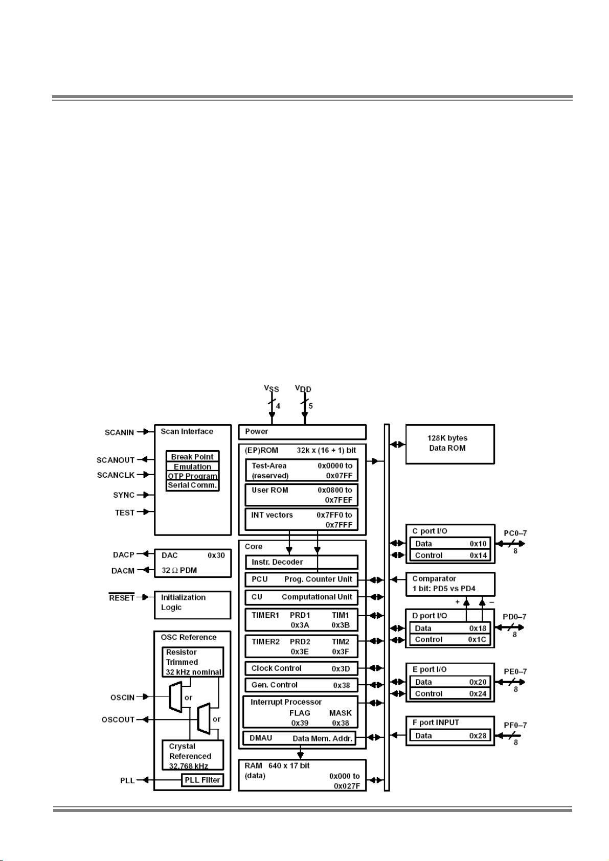
capability. The functional block diagram gives an overview of the SC-601 functionality.
Functional Block Diagram
Page 3
Data Sheet
SC-601
© 2002 Sensory Inc.
P/N 80-0207-A
3
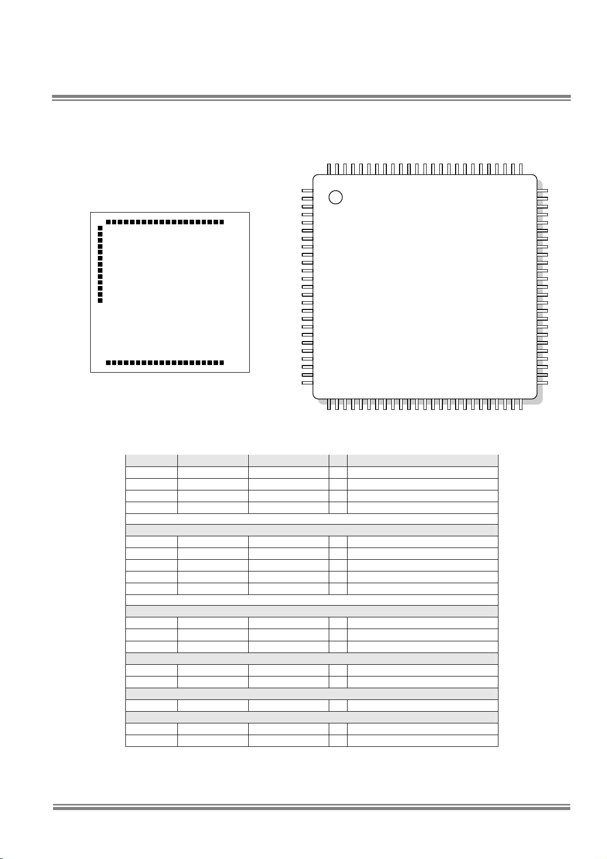
Pin/Pad Assignment
SC-601
(top view of the die)
19
20
32
33
52
1
SC-601
(100-lead LQFP)
NC
NC
NC
NC
NC
NC
NC
NC
NC
NC
NC
NC
NC
NC
NC
NC
75
74
73
72
71
70
69
68
67
66
65
60
59
58
57
56
NC
NC
NC
55
54
53
NC64
NC
NC
NC
63
62
61
NC52
NC51
26272829303132
33
4142434445
NCNCNCNCNC
VDD
VDD
SCANOUT
PE5
PE4
PE3
PE2
PE1
34353637383940
TEST
SYNC
SYNCLK
SCANIN
RESET_
PE7
PE6
4647484950
PE0
PLL
OSCIN
OSCOUT
VSS
100
9998979695949392919089
81
VSS
PD0
PD1
PD2
PD3
PD4
PD5
PD6
PD7
VDD
VSS
PC0
NC
88878685848382
PC1
PC2
PC3
PC4
PC5
PC6
PC7
8079787776
NCNCNCNCNC
NC
NC
NC
NC
DACM
VDD
DAVP
VDD
PF7
PF6
PF5
PF4
NC
1
2
3
4
5
6
7
8
9
10
11
12
20
PF3
PF2
PF1
PF0
VSS
NC
NC
13
14
15
16
17
18
19
NC
NC
NC
NC
NC
21
22
23
24
25
NAME PIN NO. PAD NO. I/O DESCRIPTION
PC0 – PC7 89 → 82 8 → 1 I/O Port C general-purpose I/O (1 Byte)
PD0 – PD7 99 → 92 18 → 11 I/O Port D general-purpose I/O (1 Byte)
PE0 – PE7 46 → 39 48 → 41 I/O Port E general-purpose I/O (1 Byte)
PF0 – PF7 16 → 9 31 → 24 I/O Port F general-purpose I/O (1 Byte)
Pins PD4 and PD4 may be dedicated to the comparator function, if the comparator enable bit is set.
Scan Port Control Signals
SCANIN 37 39 I Scan port data input
SCANOUT 33 35 O Scan port data output
SCANCLK 36 38 I Scan port clock
SYNC 35 37 I Scan port synchronization
TEST 34 36 I SC-601: test modes
The scan port pins must be bonded out on any SC-601 production board.
Reference Oscillator Signals
OSCOUT 49 51 O Resistor/crystal reference out
OSCIN 48 50 I Resistor/crystal reference in
PLL 47 49 O Phase-lock-loop filter
Digital-to-Analog Sound Output (DAC)
DACP 7 22 O Digital-to-analog plus output (+)
DACM 5 20 O Digital-to-analog minus output (–)
Initialization
RESET_ 38 40 I Initialization
Power Signals
VSS 17, 50, 90, 100† 32, 52, 9, 19† - Ground
VDD 6
†
, 8, 31, 32, 91 21†, 23, 33, 34, 10 - Processor power (+)
† The V
SS
and VDD connections service the DAC circuitry. Their pins tend to sustain a higher current draw. A dedicated decoupling capacitor
across these pins is therefore required.
Page 4
SC-601
Data sheet
4
P/N 80-0207-A
© 2002 Sensory Inc.
Absolute Maximum Ratings
Absolute maximum ratings over operating free-air temperature range (unless otherwise noted)†
Supply voltage, VDD (see Note 1) –0.3 to 7 V
Supply current, IDD (see Note 2) 35 mA
Input voltage range, VI (see Note 1) –0.3 to VDD + 0.3 V
Output voltage range, VO (see Note 1) –0.3 to VDD + 0.3 V
Storage temperature range, TA –30ºC to 125ºC
WARNING:
Stressing the SC-601 beyond the “Absolute Maximum
Ratings” may cause permanent damage. These are
stress ratings only. Operation beyond the “Operating
Conditions” is not recommended and extended
exposure beyond the “Operating Conditions” may
affect device reliability.
NOTES: 1. Unless otherwise noted, all voltages are measured with respect to VSS.
2. The total supply current includes the current out of all the I/O pins as well as the operating current of the device.
Recommended Operating Conditions
MIN MAX UNIT
Supply voltage (with respect to VSS), VDD 3 5.2 V
CPU clock rate (as programmed), f
(CPU)
64 12,320 kHz
Load resistance between DACP and DAC
M
,
R
(DAC)
32
Ω
Operating free-air temperature, TA Device functionality 0 70
°C
Timing Requirements
MIN MAX UNIT
t
(RESET)
Reset low pulse width, while VDD is within specified limits 100 ns
t1
(WIDT H)
Pulse width required prior to a negative transition at pin PD3, PD5, or PF0 → PF7
‡
2 1/F
CPU
t2
(WIDT H)
Pulse width required prior to a positive transition at pin PD2 or PD4
†
2 1/F
CPU
‡ While these pins are being used as interrupt inputs.
t
(RESET)
t
(RESET)
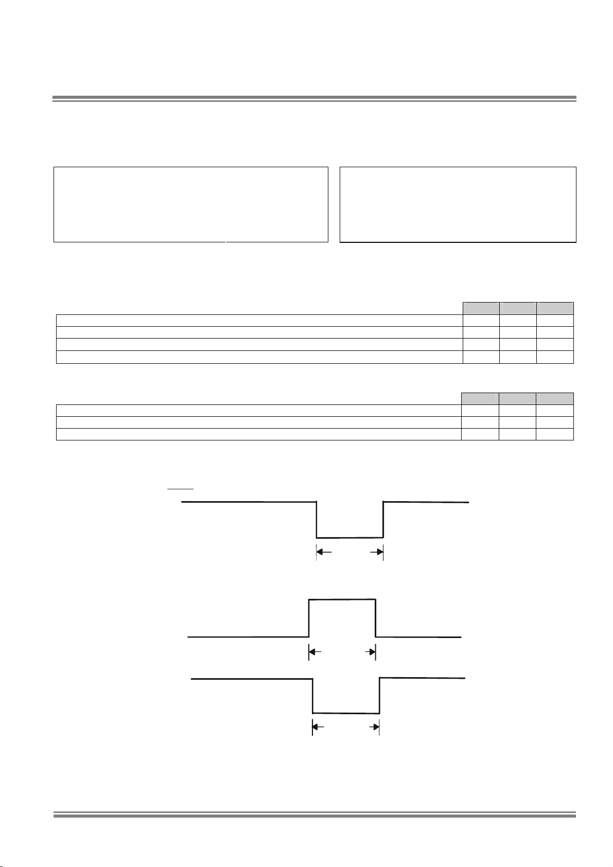
Figure 1: Initialization Timing Diagram
t1
(WIDTH)
t2
(WIDTH)
t1
(WIDTH (PD3, PD5, or F port))
t2
(WIDTH (PD2, or PD4))
Figure 2: External Interrupt Pin Pulse Width Requirements t1WIDTH and t2WIDTH
Page 5
Data Sheet
SC-601
© 2002 Sensory Inc.
P/N 80-0207-A
5
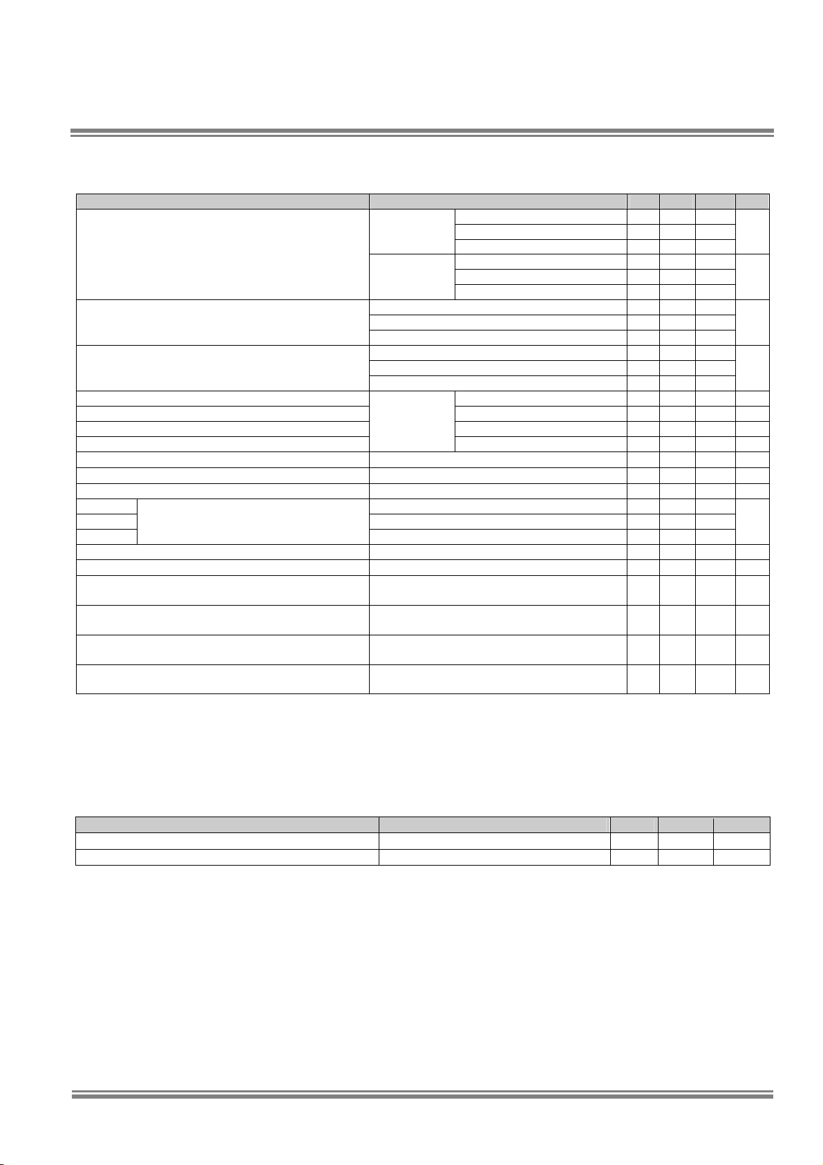
DC Electrical Characteristics, TA = 0 to 70°C
PARAMETER TEST CONDITIONS MIN TYP§MAX UNIT
Positive going threshold 2.4
Negative going threshold 1.8
VDD = 3 V
Hysteresis 0.6
V
Positive going threshold 3.3
Negative going threshold 2.9
RESET_ Threshold changes
V
DD
= 5.2 V
Hysteresis 0.4
V
VDD = 3 V 2 3
VDD = 4.5 V 3 4.5
VIH High-level input voltage
V
DD
= 5.2 V 3.5 5.2
V
VDD = 3 V 0 1
VDD = 4.5 V 0 1.5
VIL Low-level input voltage
V
DD
= 5.2 V 0 1.7
V
I
OH
¶
High-level output current per pin of I/O port VOH = 4 V –2 mA
I
OL
¶
Low-level output current per pin of I/O port VOL = 0.5 V 5 mA
I
OH (DAC)
High-level output DAC current VOH = 4 V –10 mA
I
OL (DAC)
Low-level output DAC current
V
DD
= 4.5 V
V
OL
= 0.5 V 20 mA
I
lkg
Input leakage current Excludes OSCIN 1
µA
I
(STANDBY)
Standby current RESET is low 0.05 10
µA
I
DD
†
Operating current VDD = 4.5 V, F
CLOCK
= 12.32 MHz 15 mA
I
(SLEEP-deep)
V
DD
= 4.5 V, DAC off, ARM set, OSC disabled 0.05 10
I
(SLEEP-mid)
V
DD
= 4.5 V, DAC off, ARM set, OSC enabled 40 60
I
(SLEEP-light)
Supply current
VDD = 4.5 V, DAC off, ARM clear, OSC enabled 60 100
µA
VIO Input offset voltage VDD = 4.5 V, V
ref
= 1 to 4.25 V 25 50 mV
R
(PULLUP)
F port pullup resistance VDD = 5 V 70 150
KΩ
∆f
(RTO-trim)
Trim deviation
R
RTO
= 470 KΩ, VDD = 4.5 V, TA = 25°C,
f
RTO
= 8.192 MHz (PLL setting = 7 Ch)‡
±1% ±3%
∆f
(RTO-volt)
Voltage deviation
R
RTO
= 470 KΩ, VDD = 3.5 to 5.2 V, TA = 25°C,
f
RTO
= 8.192 MHz (PLL setting = 7 Ch)‡
±1.5%
∆f
(RTO-temp)
Temperature deviation
R
RTO
= 470 KΩ, VDD = 4.5 V, TA = 0 to 70°C,
f
RTO
= 8.192 MHz (PLL setting = 7 Ch)‡
±0.03 %/°C
∆f
(RTO-res)
Resistance deviation
V
DD
= 4.5 V, TA = 25°C, R
(OSC)
= 470 KΩ at ±1%,
f
RTO
= 8.192 MHz (PLL setting = 7 Ch)‡
±1%
† Operating current assumes all inputs are tied to either VSS or VDD with no input currents due to programmed pullup resistors. The DAC
output and other outputs are open circuited.
‡ The best trim value is selected at nominal temperature and voltage but the deviation due to the trim error is ignored.
§ Typical voltage and current measurement taken at 25°C
¶ Cannot exceed 15 mA total per internal V
DD
pin. Port A, B share 1 internal VDD pin; Port C, D share 1 internal V
DD
External Component Absolute Values
PARAMETER TEST CONDITIONS MIN MAX UNIT
R
(RTO)
RTO external resistance TA = 25°C, 1% tolerance 470
KΩ
C
(PLL)
PLL external capacitance TA = 25°C, 10% tolerance 3300 pF
Page 6
SC-601
Data sheet
6
P/N 80-0207-A
© 2002 Sensory Inc.
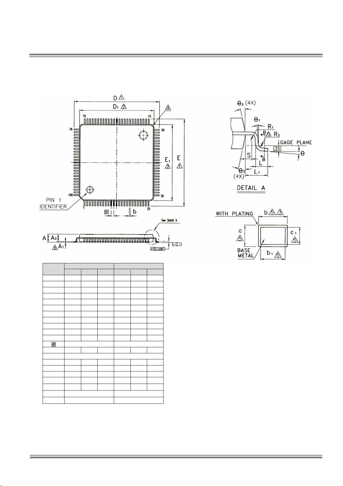
Mechanical Data
LQFP 100 PLASTICQUAD FLATPACK (14x14x1.4 mm)
Dimension in mm Dimension in inch
Symbol
Min Nom Max Min Nom Max
A - - 1.60 - - 0.063
A1 0.05 - 0.15 0.002 - 0.006
A2 1.35 1.40 1.45 0.053 0.055 0.057
b 0.17 0.22 0.27 0.007 0.009 0.011
b1 0.17 0.20 0.23 0.007 0.008 0.009
c 0.09 - 0.20 0.004 - 0.008
c1 0.09 - 0.16 0.004 - 0.006
D 15.85 16.00 16.15 0.624 0.630 0.636
D1 13.90 14.00 14.10 0.547 0.551 0.555
E 15.85 16.00 16.15 0.624 0.630 0.636
E1 13.90 14.00 14.10 0.547 0.551 0.555
0.50 BSC 0.20 BSC
L 0.45 0.60 0.75 0.018 0.024 0.030
L1 1.00 REF 0.039 BSC
R1 0.08 - - 0.003 - -
R2 0.08 - 0.20 0.003 - 0.008
S 0.20 - - 0.008 - -
›
0º 3.5º 7º 0º 3.5º 7º
›1
0º - - 0º - -
›2
12º TYP 12º TYP
›3
12º TYP 12º TYP
Notes:
A. All linear dimensions are in millimeters.
B. This drawing is subject to change without notice.
C. Falls within JEDEC MS-022
Page 7
Data Sheet
SC-601
© 2002 Sensory Inc.
P/N 80-0207-A
7
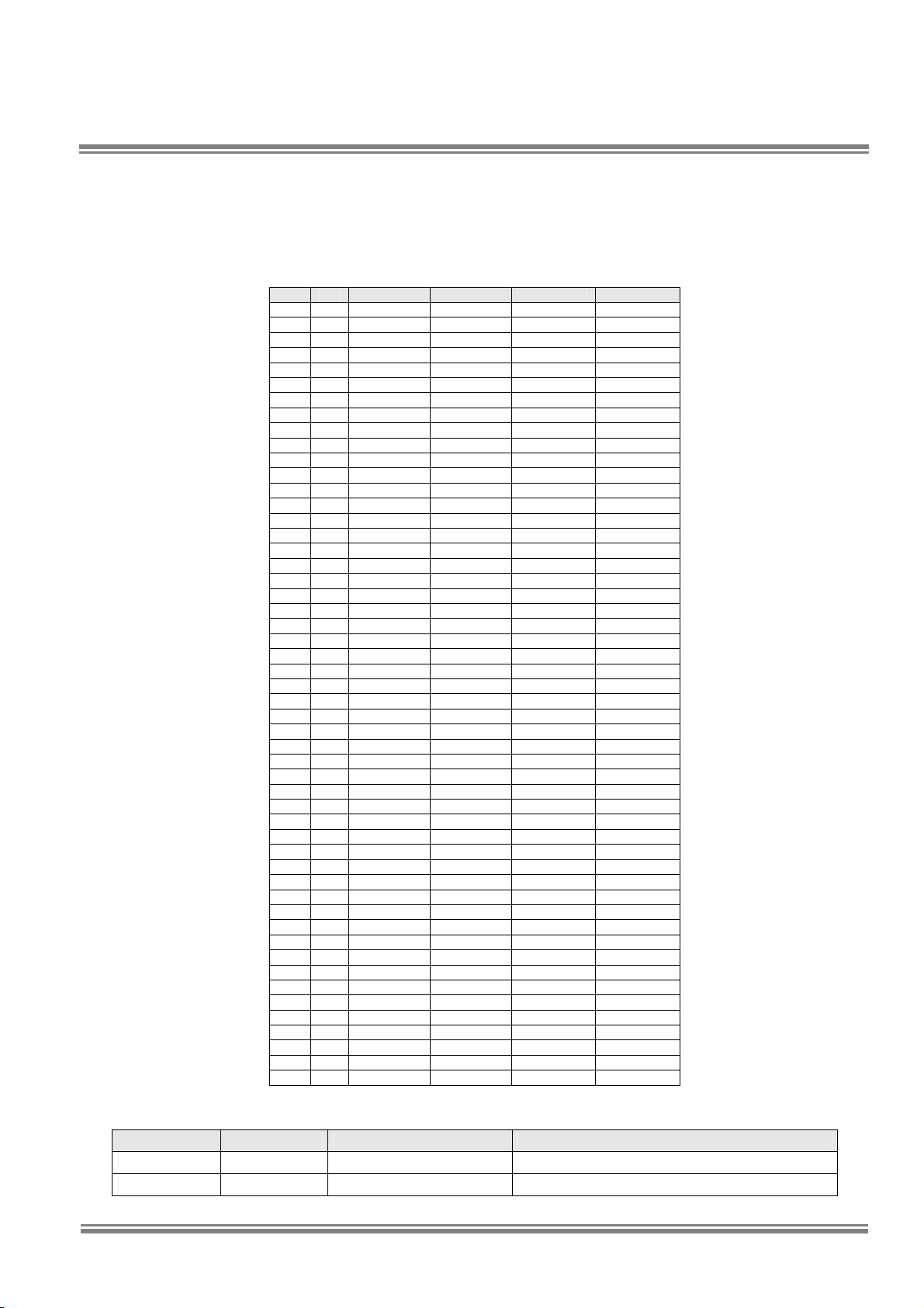
Die Bond-out Coordinates
Die Size = 144.88 x 147.64 Mil
Pad Size = 256 x 256 Mil
Units = Metric
Pad Pin X-Axis Min Y-Axis Min X-Axis Max Y-Axis Max
1 82 3402.53 622.82 3488.53 708.82
2 83 3402.53 776.82 3488.53 862.82
3 84 3402.53 930.82 3488.53 1016.82
4 85 3402.53 1084.82 3488.53 1170.82
5 86 3402.53 1238.82 3488.53 1324.82
6 87 3402.53 1392.82 3488.53 1478.82
7 88 3402.53 1546.82 3488.53 1632.82
8 89 3402.53 1700.82 3488.53 1786.82
9 90 3381.68 1852.09 3467.68 1938.09
10 91 3380.92 1957.97 3466.92 2043.97
11 92 3402.53 2110.12 3488.53 2196.12
12 93 3402.53 2264.12 3488.53 2350.12
13 94 3402.54 2418.12 3488.54 2504.12
14 95 3402.54 2572.12 3488.54 2658.12
15 96 3402.53 2726.12 3488.53 2812.12
16 97 3402.53 2880.12 3488.53 2966.12
17 98 3402.53 3034.12 3488.53 3120.12
18 99 3402.53 3188.12 3488.53 3274.12
19 100 3370.73 3325.11 3456.73 3411.11
20 5 3174.50 3395.51 3260.50 3481.51
21 6 3066.70 3395.62 3152.70 3481.62
22 7 2958.55 3395.51 3044.55 3481.51
23 8 2825.20 3395.61 2911.20 3481.61
24 9 2696.92 3426.74 2782.92 3512.74
25 10 2591.16 3426.74 2677.16 3512.74
26 11 2486.92 3426.74 2572.92 3512.74
27 12 2381.16 3426.74 2467.16 3512.74
28 13 2276.92 3426.74 2362.92 3512.74
29 14 2171.16 3426.74 2257.16 3512.74
30 15 2066.92 3426.74 2152.92 3512.74
31 16 1961.16 3426.74 2047.16 3512.74
32 17 1829.33 3396.38 1915.33 3482.38
33 31 133.08 3075.02 219.08 3161.02
34 32 133.08 2959.97 219.08 3045.97
35 33 111.44 2843.09 197.44 2929.09
36 34 111.44 2731.75 197.44 2817.75
37 35 111.44 2615.10 197.44 2701.10
38 36 111.44 2503.80 197.44 2589.80
39 37 111.44 2392.50 197.44 2478.50
40 38 111.44 2249.28 197.44 2335.28
41 39 111.47 2088.83 197.47 2174.83
42 40 111.47 1934.83 197.47 2020.83
43 41 111.47 1780.83 197.47 1866.83
44 42 111.47 1626.83 197.47 1712.83
45 43 111.47 1472.83 197.47 1558.83
46 44 111.47 1318.83 197.47 1404.83
47 45 111.47 1164.84 197.47 1250.84
48 46 111.47 1010.84 197.47 1096.84
49 47 111.44 897.45 197.44 983.45
50 48 111.44 786.15 197.44 872.15
51 49 111.44 674.88 197.44 760.88
52 50 132.30 565.86 218.30 651.86
Ordering Information
Part Ordering P/N Shipping P/N Description
SC-601 DIE
SC601-R
65-xxxx-x (ROM specific) Tested, Singulated SC-601 die in waffle pack.
SC-601 LQFP
SC601-RL1
65-xxxx-x (ROM specific) SC-601 100 pin 14x14x1.4mm LQFP
Page 8

1991 Russell Ave., Santa Clara, CA 95054
Tel: (408) 327-9000 Fax: (408) 727-4748
© 2001 SENSORY, INC. ALL RIGHT RESERVED.
Sensory is registered by the U.S. Patent and
Trademark Office.
All other trademarks or registered trademarks are the
property of their respective owners.
www.sensoryinc.com
The Interactive Speech™ Product Line
The Interactive Speech line of ICs and software was developed to “bring life to products” through advanced speech recognition and audio
technology.
The Interactive Speech Product Line was designed for consumer telephony products and cost-sensitive consumer electronic applications
such as home electronics, personal security, and personal communication.
The product line includes award-winning RSC series general-purpose microcontrollers and tools, SC series of speech microcontrollers, plus
a line of easy-to-implement chips that can be pin-configured or controlled by an external host microcontroller. Sensory’s software
technologies run on a variety of microcontrollers and DSPs.
RSC Microcontrollers and Tools
The RSC product line contains low-cost 8-bit speech-optimized microcontrollers designed for use in consumer
electronics. All members of the RSC family are fully integrated and include A/D, pre-amplifier, D/A, ROM, and RAM
circuitry. The RSC family can perform a full range of speech/audio functions including speech recognition, speaker
verification, speech and music synthesis, and voice record/playback. The family is supported by a complete suite of
evaluation tools and development kits.
SC Microcontrollers and Tools
The SC-6x product line features the highest quality speech synthesis ICs at the lowest data rate in the industry. The line includes a
12.32 MIPS processor for high-quality low data-rate speech compression and MIDI music synthesis, with plenty of power left over for
other processor and control functions. Members of the SC-6x line can store as much as 37 minutes of speech on chip and include as
much as 64 I/O pins for external interfacing. Integrating this broad range of features onto a single chip enables developers to create
products with high quality, long duration speech at very competitive price points.
Application Specific Standard Products (ASSPs)
Voice Direct™ 364 provides inexpensive speaker-dependent speech recognition and speech synthesis. This easy-to-use, pinconfigurable chip requires no custom programming and can recognize up to 60 trained words in slave mode, and 15 words in standalone mode. Ideal for speaker-dependent command and control of household consumer products, Voice Direct 364 is part of a complete
product line that includes the IC, module, and Voice Direct 364 Speech Recognition Kit.
Voice Extreme™ simplifies the creation of fully custom speech-enabled products by offering developers the capability of
programming the chip in a high-level C-like language. Program code, speech data, and even record and playback
information can be stored on a single off-chip Flash memory. Based on Sensory's RSC-364 speech processor, Voice
Extreme includes a highly efficient on-chip code interpreter, and is supported by a comprehensive suite of low-cost
development tools.
Software and Technology
Voice Activation™ micro footprint software provides advanced speech technology on a variety of microcontroller and DSP
platforms. A flexible design with a broad range of technologies allows manufacturers to easily integrate speech functionality
into consumer electronic products.
Fluent Speech™ small footprint software recognizes up to 50,000 words; offers Animated Speech with the ability to automate
enunciation and articulation; performs text-to-speech synthesis in either male or female voices; provides noise and echo cancellation,
performs Wordspotting for natural language usage; offers telephone barge-in; and provides continuous digit recognition.
Important notices
Reasonable efforts have been made to verify the accuracy of information contained herein, however no guarantee can be made of
accuracy or applicability. Sensory reserves the right to change any specification or description contained herein. Sensory reserves the
right to make changes to or to discontinue any product or service identified in this publication at any time without notice in order to
improve design and supply the best possible product. Sensory does not assume responsibility for use of any circuitry other than circuitry
entirely embodied in a Sensory product. Information contained herein is provided gratuitously and without liability to any user.
Reasonable efforts have been made to verify the accuracy of this information but no guarantee whatsoever is given as to the accuracy
or as to its applicability to particular uses. Applications described in this data sheet are for illustrative purposes only, and Sensory makes
no warranties or representations that the RSC/SC series of products will be suitable for such applications. In every instance, it must be
the responsibility of the user to determine the suitability of the products for each application. Sensory products are not authorized for use
as critical components in life support devices or systems. Sensory conveys no license or title, either expressed or implied, under any
patent, copyright, or mask work right to the RSC series of products, and Sensory makes balance between recognition and synthesis no
warranties or representations that the RSC series of products are free from patent, copyright, or mask work right infringement, unless
otherwise specified. Nothing contained herein shall be construed as a recommendation to use any product in violation of existing
patents or other rights of third parties. The sale of any Sensory product is subject to all Sensory Terms and Conditions of Sales and
Sales Policies.
 Loading...