

查询NUP2105L-D供应商
NZL5V6ATT1
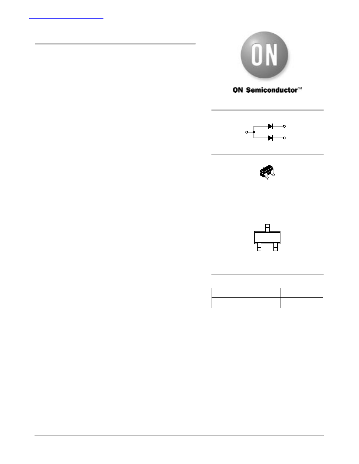
SC75 Dual Common Anode
Zener for ESD Protection
This dual monolithic silicon voltage suppressor is designed for
applications requiring transient overvoltage protection capability. It is
intended for use in voltage and ESD sensitive equipment such as
computers, printers, business machines, communication systems,
medical equipment, and other applications. Its dual junction common
anode design protects four separate lines using only one package.
These devices are ideal for situations where board space is at a
premium.
Specification Features
• SC−75 Package Allows Two Separate Unidirectional Configurations
• Low Leakage < 1 A @ 3 Volt
• Breakdown Voltage: 5.3−5.9 Volt @ 1 mA
• Low Capacitance (40 pF typical between terminals)
• ESD Protection Meeting IEC61000−4−2
Mechanical Characteristics
• Void Free, Transfer−Molded, Thermosetting Plastic Case
• Corrosion Resistant Finish, Easily Solderable
• Package Designed for Optimal Automated Board Assembly
• Small Package Size for High Density Applications
http://onsemi.com
3
ANODE
3
1
SC−75
CASE 463
STYLE 4
MARKING DIAGRAM
56
CATHODE
1
2
CATHODE
2
56 = Device Marking
ORDERING INFORMATION
Device Package Shipping
NZL5V6ATT1 SC−75 3000/Tape & Reel
Semiconductor Components Industries, LLC, 2002
February, 2001 − Rev. 1
1 Publication Order Number:
NZL5V6ATT1/D
NZL5V6ATT1
ELECTRICAL CHARACTERISTICS
(TA = 25°C unless otherwise noted)
UNIDIRECTIONAL (Circuit tied to Pins 1 and 3 or 2 and 3)
Symbol
V
V
I
PP
V
RWM
I
V
I
I
V
Z
I
ZK
Z
Maximum Reverse Peak Pulse Current
Clamping Voltage @ I
C
Working Peak Reverse Voltage
Maximum Reverse Leakage Current @ V
R
Breakdown Voltage @ I
BR
Test Current
T
Maximum Temperature Coefficient of V
BR
Forward Current
F
Forward Voltage @ I
F
Maximum Zener Impedance @ I
ZT
Reverse Current
Maximum Zener Impedance @ I
ZK
MAXIMUM RATINGS (T
Steady State Power − 1 Diode (Note 1) P
Maximum Junction Temperature T
Operating Junction and Storage Temperature Range TJ T
ESD Discharge IEC61000−4−2, Air Discharge
Lead Solder Temperature (10 seconds duration) T
Parameter
PP
T
BR
F
ZT
ZK
= 25°C unless otherwise noted)
A
Characteristic
IEC61000−4−2, Contact Discharge
RWM
I
I
F
V
VCV
BR
RWM
I
V
R
F
I
T
I
PP
V
Uni−Directional TVS
Symbol Value Unit
150 mW
150 °C
−55 to +150 °C
15
kV
8
260 °C
Jmax
V
PP
D
stg
L
ELECTRICAL CHARACTERISTICS
Typical
Breakdown Voltage
V
@ 1 mA (Volts)
BR
Leakage Current
I
@ VRM = 3.0 V
RM
Device Min Nom Max (A) (pF) (V)
NZL5V6 5.3 5.6 5.9 1.0 40 1.25
1. Only 1 diode under power. For all 4 diodes under power, PD will be 25%. Mounted on FR−4 board with min pad.
300
250
200
100
90
80
70
t
r
60
150
50
40
100
50
, POWER DISSIPATION (mW)
D
P
0
0 25 50 75 100 125 150 175
30
20
% OF PEAK PULSE CURRENT
10
0
t
p
0 20406080
TEMPERATURE (°C)
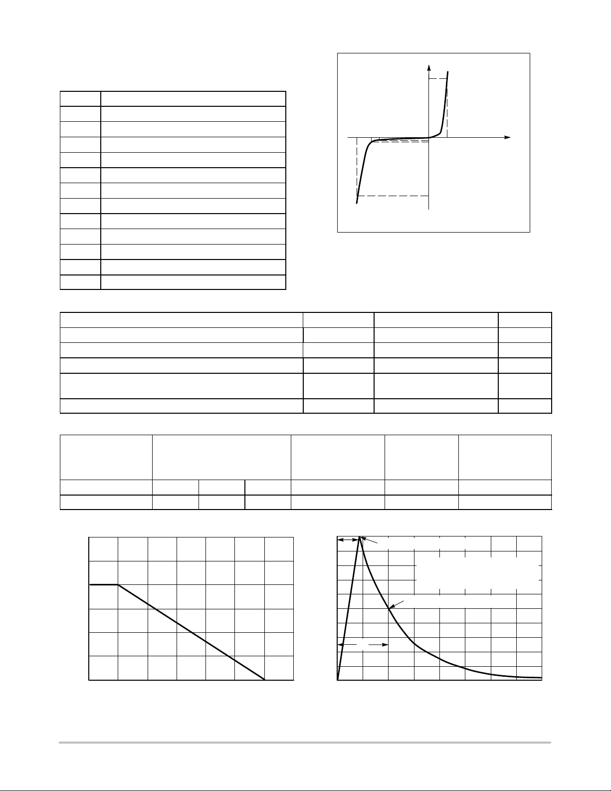
Figure 1. Steady State Power Derating Curve
Figure 2. 8 X 20 s Pulse Waveform
Capacitance
@ 0 V Bias
@ 1 MHz
PEAK VALUE I
PULSE WIDTH (tp) IS DEFINED
AS THAT POINT WHERE THE
PEAK CURRENT DECAY = 8 s
HALF VALUE I
t, TIME (s)
RSM
@ 8 s
V
/2 @ 20 s
RSM
Max
@ IF = 10 mA
F
http://onsemi.com
2

NZL5V6ATT1
100
10
, PEAK POWER (W)
PK
P
NOTE: Non−Repetitive Surge
1
10 100 1000
tp, PULSE WIDTH (s)
Figure 3. Pulse Rating Curve
1
0.1
45
40
35
30
25
20
15
1 MHz FREQUENCY
10
TYPICAL CAPACITANCE (pF)
5
0
0 0.5 1 1.5 5
2.52
3 3.5 4.54
BIAS VOLTAGE (V)
Figure 4. Capacitance
100
10
0.01
, FORWARD CURRENT (A)
F
I
0.001
0.6 1 1.4
0.7 0.8 0.9 1.1 1.2 1.3
VF, FORWARD VOLTAGE (V)
Figure 5. Forward Current versus
Forward Voltage
, PEAK PULSE CURRENT (A)
PP
I
1
4 4.2 4.4 4.6 6
4.8 5
VC, CLAMPING VOLTAGE (V)
1.0 s SQUARE WAVE
5.2 5.4
5.6 5.8
Figure 6. Clamping Voltage versus Peak Pulse
Current (Reverse Direction)
http://onsemi.com
3

S
D
3 PL
0.20 (0.008) B
M
J
−A−
3
L
NZL5V6ATT1
PACKAGE DIMENSIONS
SC−75 (SC−90, SOT−416)
CASE 463−01
ISSUE B
NOTES:
1. DIMENSIONING AND TOLERANCING PER ANSI
2
G
−B−
1
0.20 (0.008) A
K
C
H
Y14.5M, 1982.
2. CONTROLLING DIMENSION: MILLIMETER.
DIM MIN MAX MIN MAX
A 0.70 0.80 0.028 0.031
B 1.40 1.80 0.055 0.071
C 0.60 0.90 0.024 0.035
D 0.15 0.30 0.006 0.012
G 1.00 BSC 0.039 BSC
H −−− 0.10 −−− 0.004
J 0.10 0.25 0.004 0.010
K 1.45 1.75 0.057 0.069
L 0.10 0.20 0.004 0.008
S 0.50 BSC 0.020 BSC
STYLE 4:
PIN 1. CATHODE
2. CATHODE
3. ANODE
INCHESMILLIMETERS
ON Semiconductor and are trademarks of Semiconductor Components Industries, LLC (SCILLC). SCILLC reserves the right to make changes
without further notice to any products herein. SCILLC makes no warranty, representation or guarantee regarding the suitability of its products for any particular
purpose, nor does SCILLC assume any liability arising out of the application or use of any product or circuit, and specifically disclaims any and all liability,
including without limitation special, consequential or incidental damages. “Typical” parameters which may be provided in SCILLC data sheets and/or
specifications can and do vary in different applications and actual performance may vary over time. All operating parameters, including “Typicals” must be
validated for each customer application by customer’s technical experts. SCILLC does not convey any license under its patent rights nor the rights of others.
SCILLC products are not designed, intended, or authorized for use as components in systems intended for surgical implant into the body, or other applications
intended to support or sustain life, or for any other application in which the failure of the SCILLC product could create a situation where personal injury or
death may occur. Should Buyer purchase or use SCILLC products for any such unintended or unauthorized application, Buyer shall indemnify and hold
SCILLC and its officers, employees, subsidiaries, affiliates, and distributors harmless against all claims, costs, damages, and expenses, and reasonable
attorney fees arising out of, directly or indirectly, any claim of personal injury or death associated with such unintended or unauthorized use, even if such claim
alleges that SCILLC was negligent regarding the design or manufacture of the part. SCILLC is an Equal Opportunity/Affirmative Action Employer.
PUBLICATION ORDERING INFORMATION
Literature Fulfillment:
Literature Distribution Center for ON Semiconductor
P.O. Box 5163, Denver, Colorado 80217 USA
Phone: 303−675−2175 or 800−344−3860 Toll Free USA/Canada
Fax: 303−675−2176 or 800−344−3867 Toll Free USA/Canada
Email: ONlit@hibbertco.com
N. American Technical Support: 800−282−9855 Toll Free USA/Canada
http://onsemi.com
JAPAN: ON Semiconductor, Japan Customer Focus Center
4−32−1 Nishi−Gotanda, Shinagawa−ku, Tokyo, Japan 141−0031
Phone: 81−3−5740−2700
Email: r14525@onsemi.com
ON Semiconductor Website: http://onsemi.com
For additional information, please contact your local
Sales Representative.
NZL5V6ATT1/D
4
 Loading...