

查询NUP4201DR2 供应商
NUP4201DR2
Advance Information
Low Capacitance Surface
Mount TVS for High-Speed
Data Interfaces
The NUP4201DR2 transient voltage suppressor is designed to
protect equipment attached to high speed communication lines from
ESD, EFT, and lighting.
Features:
• SO–8 Package
• Peak Power – 500 Watts 8 x 20 S
• ESD Rating:
IEC 61000–4–2 (ESD) 15 kV (air) 8 kV (contact)
IEC 61000–4–4 (EFT) 40 A (5/50 ns)
IEC 61000–4–5 (lighting) 23 (8/20 s)
• UL Flammability Rating of 94V–0
T ypical Applications:
• High Speed Communication Line Protection
• USB Power and Data Line Protection
• Video Line Protection
• Base Stations
• HDSL, IDSL Secondary IC Side Protection
• Microcontroller Input Protection
http://onsemi.com
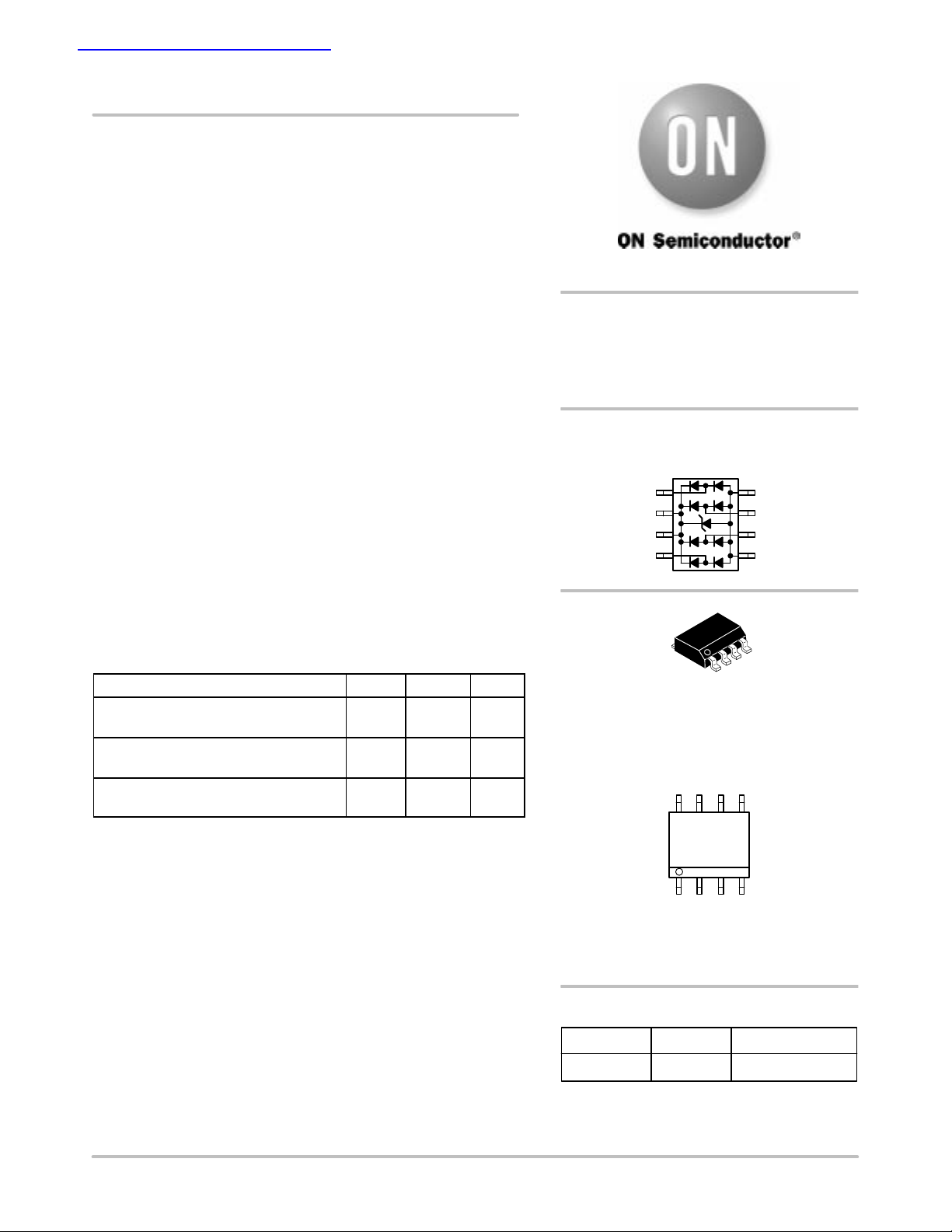
SO–8 LOW CAPACITANCE
VOLTAGE SUPPRESSOR
500 WATTS PEAK POWER
6 VOLTS
PIN CONFIGURATION
AND SCHEMATIC
I/O 1 1
REF 1 2
REF 1 3
I/O 2 4
8 REF 2
7 I/O 4
6 I/O 3
5 REF 2
MAXIMUM RATINGS
Rating Symbol Value Unit
Peak Power Dissipation
8 x 20 S @ T
Junction and Storage
Temperature Range
Lead Solder Temperature –
Maximum 10 Seconds Duration
1. Non–repetitive current pulse 8 x 20 S exponential decay waveform
This document contains information on a new product. Specifications and information
herein are subject to change without notice.
= 25°C (Note 1)
A
P
TJ, T
T
stg
500 W
–55 to
+150
260 °C
pk
L
°C
8
1
SO–8
CASE 751
PLASTIC
MARKING DIAGRAM
P4201
LYW
P4201 = Device Code
L = Location Code
Y = Year
W = Work Week
ORDERING INFORMATION
Device Package Shipping
NUP4201DR2 SO–8 2500/Tape & Reel
Semiconductor Components Industries, LLC, 2002
April, 2002 – Rev. 0
1 Publication Order Number:
NUP4201DR2/D
NUP4201DR2
ELECTRICAL CHARACTERISTICS
Characteristic Symbol Min Typ Max Unit
Reverse Breakdown Voltage @ It = 1.0 mA V
Reverse Leakage Current @ V
= 5.0 Volts I
RWM
Maximum Clamping Voltage @ IPP = 1.0 A, 8 x 20 S V
Maximum Clamping Voltage @ IPP = 10 A, 8 x 20 S V
BR
R
C
C
Between I/O Pins and Ground @ DC Bias = 0 V, 1.0 MHz Capacitance – 5.0 10 pF
Between I/O Pins and I/O @ DC Bias = 0 V, 1.0 MHz Capacitance – 2.5 5.0 pF
6.0 – – V
N/A – 10 A
N/A – 9.8 V
N/A – 12 V
ELECTRICAL CHARACTERISTICS
(TA = 25°C unless otherwise noted)
UNIDIRECTIONAL (Circuit tied to Pins 1 and 3 or 2 and 3)
Symbol
I
PP
V
C
V
RWM
I
R
V
BR
I
T
V
BR
I
F
V
F
Z
ZT
I
ZK
Z
ZK
Maximum Reverse Peak Pulse Current
Clamping Voltage @ I
Working Peak Reverse Voltage
Maximum Reverse Leakage Current @ V
Breakdown Voltage @ I
Test Current
Maximum Temperature Coefficient of V
Forward Current
Forward Voltage @ I
Maximum Zener Impedance @ I
Reverse Current
Maximum Zener Impedance @ I
Parameter
PP
RWM
T
BR
F
ZT
ZK
VCV
V
RWM
BR
Uni–Directional TVS
I
I
F
I
V
R
F
I
T
I
PP
V
http://onsemi.com
2
NUP4201DR2
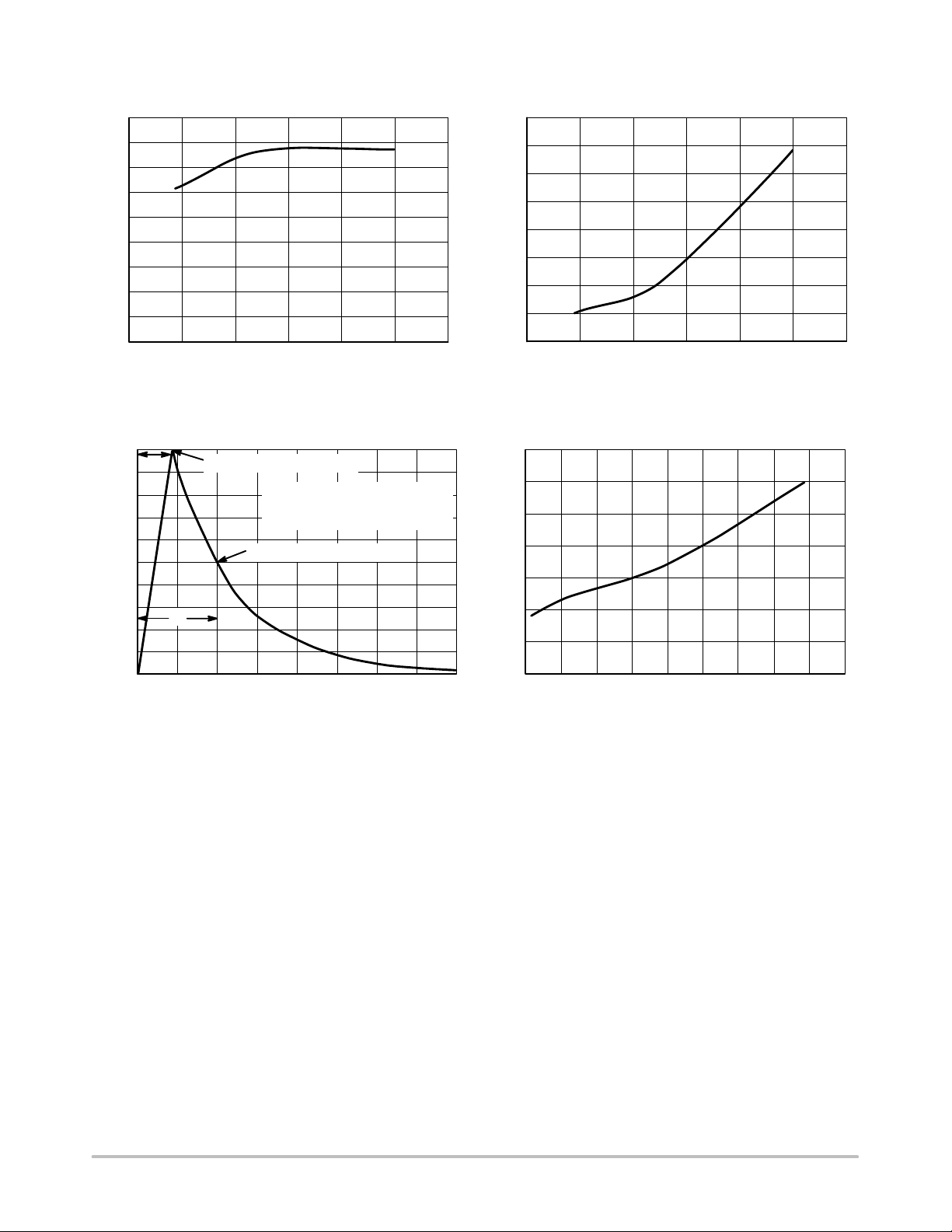
TYPICAL CHARACTERISTICS
9
8
7
6
5
4
3
2
, REVERSE BREAKDOWN (V)
Z
V
1
0
–100 0
–50
50 150
T, TEMPERATURE (°C)
100 200
Figure 1. Reverse Breakdown versus
Temperature
100
t
r
90
80
70
60
50
40
30
20
% OF PEAK PULSE CURRENT
10
0
0204060
PEAK VALUE I
t
P
@ 8 s
RSM
PULSE WIDTH (tP) IS DEFINED
AS THAT POINT WHERE THE
PEAK CURRENT DECAY = 8 s
HALF VALUE I
t, TIME (s)
/2 @ 20 s
RSM
Figure 3. 8 × 20 s Pulse Waveform
80
8
7
6
5
4
3
2
, REVERSE LEAKAGE (A)
R
I
1
0
–100 –50 50 100
0 150
T, TEMPERATURE (°C)
Figure 2. Reverse Leakage versus
Temperature
35
30
25
20
15
10
, CLAMPING VOLTAGE (V)
C
V
5
0
0204060
10 30 50 70 90
I
, PEAK PULSE CURRENT (A)
PP
Figure 4. Clamping Voltage versus Peak Pulse
Current
200
80
http://onsemi.com
3
NUP4201DR2
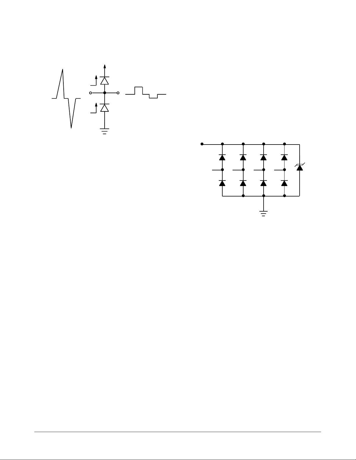
Applications information
The new NUP4201DR2 device is a low capacitance TVS
Diode array designed to protect sensitive electronics such as
communications systems, computers, and computer
peripherals against damage due to ESD conditions or
transient voltage conditions. Because of its low capacitance
array configuration, it can be used in high speed I/O data
lines.
The integrated design of the NUP4201DR2 device offers
surge rated, low capacitance steering diodes and a TVS
diode integrated in a single package (SO–8). If a transient
condition occurs, the steering diodes will drive the transient
condition to the positive polarity of the power supply or to
ground. The TVS device protects the power line against
over–voltage conditions to avoid damage in any
downstream components.
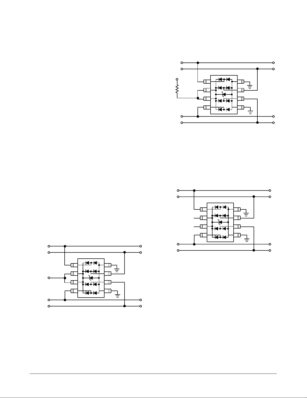
NUP4201DR2 Device’s Configurations Options
The NUP4201DR2 is able to protect up to four data lines
against transient over–voltage conditions by driving them to
a fixed reference point for clamping purposes. The steering
diodes will be forward biased whenever the voltage on the
protected line exceeds the reference voltage (Vcc+Vf). The
diodes will drive the transient current away from the
sensitive circuit.
Data lines are connected at pins 1,4,6 and 7. The negative
reference is connected at pins 5 and 8. These pins must be
connected directly to ground by using a ground plane to
minimize the PCB’s ground inductance. It is very important
to reduce as much as possible the PCB trace lengths to
minimize parasitic inductances.
Option 1
Four Data lines protection and power supply protection
using Vcc as reference.
Option 2
Four Data lines protection with Bias and power supply
isolation resistor.
I/O 1
I/O 2
V
CC
10 K
1
2
3
4
I/O 3
I/O 4
8
7
6
5
The NUP4201DR2 device can be isolated from the power
supply by connecting a series resistor between pins 2 & 3 and
Vcc. A resistor of 10Kohms is recommended for isolation
purposes. The internal TVS and steering diodes remain
biased, which provides the advantage of lower capacitance.
Option 3
Four Data lines protection using internal TVS diode as
reference.
I/O 1
I/O 2
NC
NC
1
2
3
4
8
7
6
5
I/O 1
I/O 2
V
CC
I/O 3
I/O 4
1
2
3
4
8
7
6
5
For this configuration, connect pins 2 & 3 directly to the
positive supply rail (Vcc), the data lines are referenced to the
supply voltage. The internal TVS diode prevents
over–voltage on the supply rail.
http://onsemi.com
I/O 3
I/O 4
In the case of applications in which a positive supply
reference is not available or full isolation is required, the
internal TVS could be used as the reference, so for this
purpose, the pins 2 and 3 are not connected. In this case, the
steering diodes will conduct whenever the voltage on the
protected line exceeds the working voltage of the TVS plus
one diode drop (Vc=Vf + V
4
TVS).
NUP4201DR2
“Rail to Rail” Protection Topology
The following figure shows a case when discrete diodes
are configured for rail to rail protection on an I/O line:
V
CC
ESD
Positive
ESD
Negative
11
12
D1
D2
VF + V
CC
–VF
Upon the above figure, it is possible to observe that if a
positive ESD condition occurs, the D1 diode will be forward
biased while the D2 diode will be biased when a negative
ESD condition occurs. A valid first approximation of the
resulting clamping voltage due to the protection diodes can
be made as follows:
For positive pulse conditions:
Vc = Vcc + Vf
For negative pulse conditions:
Vc = –Vf
It is important to mention that effects of parasitic
inductances must be considered for fast rise time transient
conditions because the clamping voltage on the protected
circuit will be different than in the previous case. A valid
approximation of the resulting clamping voltage can be
made as show below:
For positive pulse conditions:
Vc = Vcc + Vf + (L di
ESD/dt)
For negative pulse conditions:
Vc = –Vf – (L diESD/dt)
As shown in the formulas, the clamping voltage (Vc) not
only depends on the Vf of the steering diodes but also in the
L di
ESD/dt factor, so this is why it is very important to have
a good board layout to minimize the effects of the parasitic
inductances.
Nevertheless, some disadvantages are still present when
discrete diodes are used to suppress ESD conditions in “rail
to rail” configuration. If the ESD current is too high, it can
potentially result in the damage of any components
connected to that rail and it is also possible to experience
damage in the discrete diodes if their power dissipation
capability is exceeded.
The NUP4201DR2 On Semiconductor’s device provides
a concept named “RailClamp” which is designed to
eliminate the disadvantages of the usage of discrete diodes
for ESD protection. The RailClamp concept is achieved
with the integration of the TVS device in together with the
steering diodes.
D1
D2
Rail to Rail Protection with integrated TBS to achieve the
RailClamp concept
D3
D4
D5
D6
D7
D8
0
During an ESD condition, the ESD current will be driven
to ground through the TVS device, so the resulting clamping
voltage on the protected IC will be:
Vc = VF(RailClamp) + VTVS.
The clamping voltage of the TVS device is shown as part
of the specifications of the NUP4201DR2 datasheet. The
clamping voltage will depend on the magnitude of the ESD
current. The steering diodes are fast switching devices with
unique forward voltage and low capacitance characteristics.
http://onsemi.com
5

UPSTREAM
USB PORT
V
BUS
D+
D–
GND
V
BUS
NUP2201DT1
V
BUS
NUP4201DR2
Typical Applications
USB
Controller
C
C
V
BUS
V
R
T
R
T
V
BUS
C
T
T
R
T
R
T
NUP4201DR2
BUS
D+
DOWNSTREAM
D–
USB PORT
GND
V
BUS
V
BUS
DOWNSTREAM
D+
D–
USB PORT
GND
C
T
T
RTIP
RRING
T1/E1
TRANCEIVER
TTIP
TRING
ESD Protection for USB Port
V
CC
TI/E1 Interface Protection
R1
R3
R2
NUP4201DR2
R4
R5
T1
T2
http://onsemi.com
6
NUP4201DR2
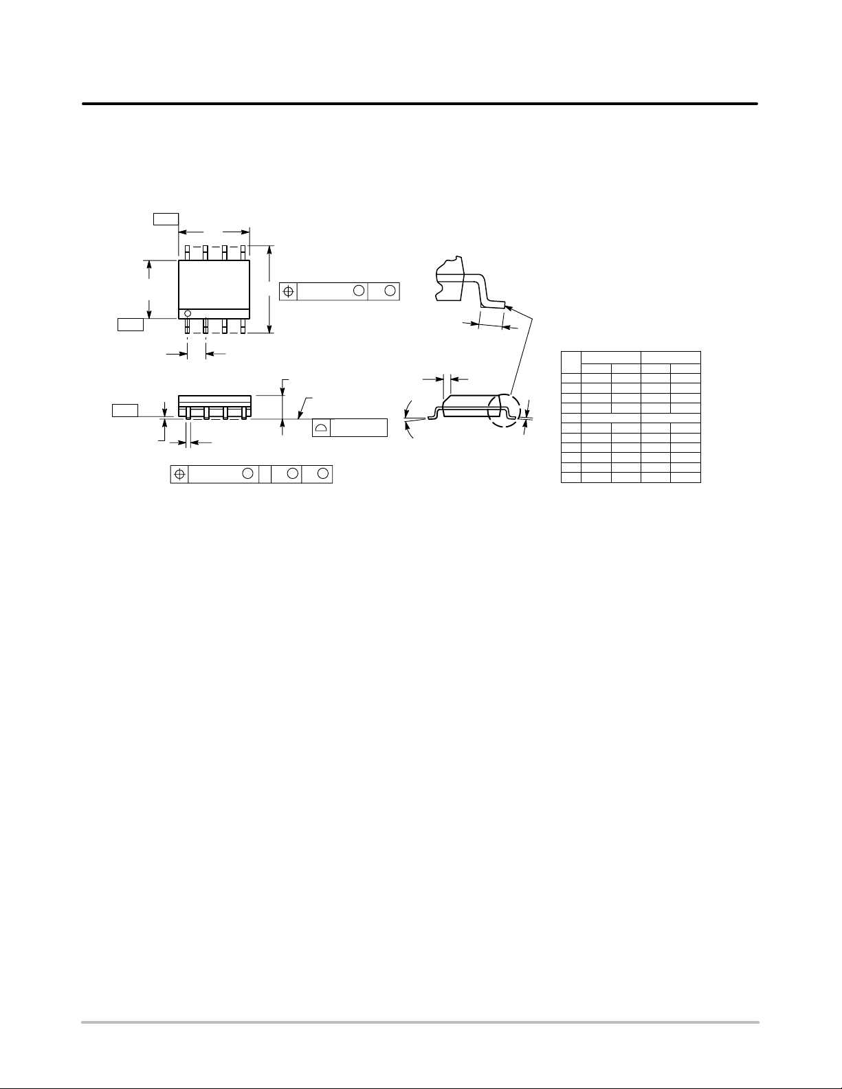
Transient Voltage Suppressor – Surface Mount
500 Watts Peak Power
SO–8
CASE 751–07
ISSUE W
–Y–
–Z–
–X–
A
58
B
1
S
0.25 (0.010)
4
M
M
Y
K
G
C
SEATING
PLANE
0.10 (0.004)
H
D
0.25 (0.010) Z
M
Y
SXS
N
X 45
M
NOTES:
1. DIMENSIONING AND TOLERANCING PER ANSI
Y14.5M, 1982.
2. CONTROLLING DIMENSION: MILLIMETER.
3. DIMENSION A AND B DO NOT INCLUDE MOLD
PROTRUSION.
4. MAXIMUM MOLD PROTRUSION 0.15 (0.006) PER
SIDE.
5. DIMENSION D DOES NOT INCLUDE DAMBAR
PROTRUSION. ALLOWABLE DAMBAR
PROTRUSION SHALL BE 0.127 (0.005) TOTAL IN
EXCESS OF THE D DIMENSION AT MAXIMUM
MATERIAL CONDITION.
MILLIMETERS
DIMAMIN MAX MIN MAX
4.80 5.00 0.189 0.197
B 3.80 4.00 0.150 0.157
C 1.35 1.75 0.053 0.069
D 0.33 0.51 0.013 0.020
G 1.27 BSC 0.050 BSC
H 0.10 0.25 0.004 0.010
J
J 0.19 0.25 0.007 0.010
K 0.40 1.27 0.016 0.050
M 0 8 0 8
N 0.25 0.50 0.010 0.020
S 5.80 6.20 0.228 0.244
INCHES
http://onsemi.com
7

NUP4201DR2
ON Semiconductor and are registered trademarks of Semiconductor Components Industries, LLC (SCILLC). SCILLC reserves the right to make
changes without further notice to any products herein. SCILLC makes no warranty, representation or guarantee regarding the suitability of its products for any
particular purpose, nor does SCILLC assume any liability arising out of the application or use of any product or circuit, and specifically disclaims any and all
liability, including without limitation special, consequential or incidental damages. “Typical” parameters which may be provided in SCILLC data sheets and/or
specifications can and do vary in different applications and actual performance may vary over time. All operating parameters, including “Typicals” must be
validated for each customer application by customer’s technical experts. SCILLC does not convey any license under its patent rights nor the rights of others.
SCILLC products are not designed, intended, or authorized for use as components in systems intended for surgical implant into the body, or other applications
intended to support or sustain life, or for any other application in which the failure of the SCILLC product could create a situation where personal injury or death
may occur. Should Buyer purchase or use SCILLC products for any such unintended or unauthorized application, Buyer shall indemnify and hold SCILLC
and its officers, employees, subsidiaries, affiliates, and distributors harmless against all claims, costs, damages, and expenses, and reasonable attorney fees
arising out of, directly or indirectly, any claim of personal injury or death associated with such unintended or unauthorized use, even if such claim alleges that
SCILLC was negligent regarding the design or manufacture of the part. SCILLC is an Equal Opportunity/Affirmative Action Employer.
PUBLICATION ORDERING INFORMATION
Literature Fulfillment:
Literature Distribution Center for ON Semiconductor
P.O. Box 5163, Denver, Colorado 80217 USA
Phone: 303–675–2175 or 800–344–3860 Toll Free USA/Canada
Fax: 303–675–2176 or 800–344–3867 Toll Free USA/Canada
Email: ONlit@hibbertco.com
N. American Technical Support: 800–282–9855 Toll Free USA/Canada
http://onsemi.com
JAPAN: ON Semiconductor, Japan Customer Focus Center
4–32–1 Nishi–Gotanda, Shinagawa–ku, Tokyo, Japan 141–0031
Phone: 81–3–5740–2700
Email: r14525@onsemi.com
ON Semiconductor Website: http://onsemi.com
For additional information, please contact your local
Sales Representative.
NUP4201DR2/D
8
 Loading...