

查询NUP4108W5T2G供应商
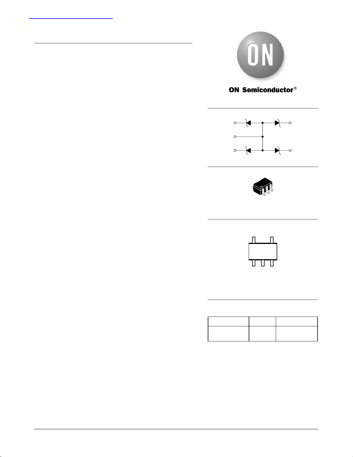
NUP4108W5
Low Capacitance
Quad Array for
ESD Protection
This integrated transient voltage suppressor device (TVS) is
designed for applications requiring transient overvoltage protection. It
is intended for use in sensitive equipment such as computers, printers,
business machines, communication systems, medical equipment, and
other applications. Its integrated design provides very effective and
reliable protection for four separate lines using only one package. This
device is ideal for situations where board space is at a premium.
http://onsemi.com
1
2
5
Features
• ESD Protection: IEC61000−4−2: Level 4
MILSTD 883C − Method 3015−6: Class 3
• Four Separate Unidirectional Configurations for Protection
• Low Leakage Current < 1 mA
• Power Dissipation: 380 mW
• Small SC−88A SMT Package
• Low Capacitance
• This is a Pb−Free Device
Benefits
• Provides Protection for ESD Industry Standards: IEC 61000, HBM
• Minimize Power Consumption of the System
• Minimize PCB Board Space
Typical Applications
• Instrumentation Equipment
• Serial and Parallel Ports
• Microprocessor Based Equipment
• Notebooks, Desktops, Servers
• Cellular and Portable Equipment
3
SC−88A/SOT−323
CASE 419A
MARKING DIAGRAM
45
RY M
G
132
RY = Specific Device Code
M = Date Code
G = Pb−Free Package
ORDERING INFORMATION
Device Package Shipping
NUP4108W5T2G SC−88A
(Pb−Free)
†For information on tape and reel specifications,
including part orientation and tape sizes, please
refer to our Tape and Reel Packaging Specifications
Brochure, BRD8011/D.
4
†
3000/Tape & Reel
© Semiconductor Components Industries, LLC, 2007
February, 2007 − Rev. 2
1 Publication Order Number:
NUP4108W5/D
NUP4108W5
MAXIMUM RATINGS (T
Peak Power Dissipation
= 25°C unless otherwise noted)
A
Rating
Symbol Value Unit
P
PK
20 W
8 20 msec Double Exponential Waveform (Note 1)
Steady State Power − 1 Diode (Note 2) P
Thermal Resistance −
R
Junction−to−Ambient
Above 25°C, Derate
Operating Junction Temperature Range T
Storage Temperature Range T
Lead Solder Temperature − Maximum 10 Seconds Duration T
q
stg
D
JA
J
L
380 mW
327
3.05
°C/W
mW/°C
−40 to +125 °C
−55 to +150 °C
260 °C
Stresses exceeding Maximum Ratings may damage the device. Maximum Ratings are stress ratings only. Functional operation above the
Recommended Operating Conditions is not implied. Extended exposure to stresses above the Recommended Operating Conditions may affect
device reliability.
1. Non−repetitive current pulse per Figure 1.
2. Only 1 diode under power. For all 4 diodes under power, PD will be 25%. Mounted on FR4 board with min pad.
ELECTRICAL CHARACTERISTICS (T
= 25°C unless otherwise noted)
A
NUP4108W5
Characteristic Symbol Min Typ Max Unit
Breakdown Voltage (IT = 1 mA) (Note 3) V
Leakage Current (V
= 5.0 V) I
RWM
Clamping Voltage 1 (IPP = 1.6 A, 8 20 msec Waveform)
Maximum Peak Pulse Current (8 20 msec Waveform)
Junction Capacitance− (VR = 0 V, f = 1 MHz)
− (VR = 3.0 V, f = 1 MHz)
3. VBR is measured at pulse test current IT.
BR
R
V
C
I
PP
C
J
6.4 6.8 7.1 V
− − 1.0
− − 13 V
− − 1.6 A
−
−
12
6.7
15
9.5
mA
pF
http://onsemi.com
2
NUP4108W5
100
10
, PEAK SURGE POWER (W)
pk
P
1
1 10 100 1000
t, TIME (ms)
Figure 1. Pulse Width
0.16
0.14
0.12
0.10
0.08
0.06
0.04
, REVERSE LEAKAGE (mA)
R
I
0.02
0
−60 0 80 100
−40 −20 604020
T, TEMPERATURE (°C)
Figure 3. Reverse Leakage versus
Temperature
110
100
PP
90
80
70
60
50
40
30
20
% OF RATED POWER OR I
10
0
TA, AMBIENT TEMPERATURE (°C)
Figure 2. Power Derating Curve
14
12
10
8
6
4
1 MHz FREQUENCY
TYPICAL CAPACITANCE (pF)
2
0
01 2 3 6
BIAS VOLTAGE (V)
TA = 25°C
45
Figure 4. Capacitance
1501251007550250
6 V
12 V
100
t
r
90
80
70
60
50
40
30
20
% OF PEAK PULSE CURRENT
10
0
020406080
t
P
PEAK VALUE I
PULSE WIDTH (tP) IS DEFINED
AS THAT POINT WHERE THE
PEAK CURRENT DECAY = 8 ms
HALF VALUE I
t, TIME (ms)
RSM
@ 8 ms
RSM
/2 @ 20 ms
Figure 5. 8 × 20 ms Pulse Waveform
http://onsemi.com
1
0.1
0.01
, FORWARD CURRENT (A)
F
I
0.001
3
TA = 25°C
1.81.61.41.21.00.80.6
VF, FORWARD VOLTAGE (V)
Figure 6. Forward Voltage
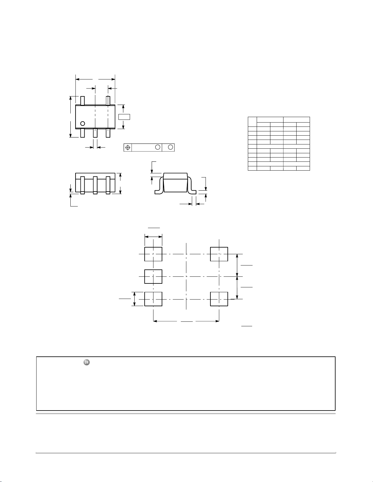
NUP4108W5
PACKAGE DIMENSIONS
SC−88A, SOT−353, SC−70
CASE 419A−02
ISSUE J
A
G
45
D 5 PL
−B−
MM
B0.2 (0.008)
S
12 3
N
NOTES:
1. DIMENSIONING AND TOLERANCING
PER ANSI Y14.5M, 1982.
2. CONTROLLING DIMENSION: INCH.
3. 419A−01 OBSOLETE. NEW STANDARD
419A−02.
4. DIMENSIONS A AND B DO NOT INCLUDE
MOLD FLASH, PROTRUSIONS, OR GATE
BURRS.
INCHES
DIMAMIN MAX MIN MAX
B 1.15 1.350.045 0.053
C 0.80 1.100.031 0.043
D 0.10 0.300.004 0.012
G 0.65 BSC0.026 BSC
H −−− 0.10−−−0.004
J 0.10 0.250.004 0.010
K 0.10 0.300.004 0.012
N 0.20 REF0.008 REF
S 2.00 2.200.079 0.087
MILLIMETERS
1.80 2.200.071 0.087
J
C
H
K
SOLDERING FOOTPRINT*
0.50
0.0197
0.65
0.025
0.65
0.025
0.40
0.0157
1.9
0.0748
SCALE 20:1
ǒ
inches
mm
Ǔ
*For additional information on our Pb−Free strategy and soldering
details, please download the ON Semiconductor Soldering and
Mounting Techniques Reference Manual, SOLDERRM/D.
ON Semiconductor and are registered trademarks of Semiconductor Components Industries, LLC (SCILLC). SCILLC reserves the right to make changes without further notice
to any products herein. SCILLC makes no warranty, representation or guarantee regarding the suitability of its products for any particular purpose, nor does SCILLC assume any liability
arising out of the application or use of any product or circuit, and specifically disclaims any and all liability, including without limitation special, consequential or incidental damages.
“Typical” parameters which may be provided in SCILLC data sheets and/or specifications can and do vary in different applications and actual performance may vary over time. All
operating parameters, including “Typicals” must be validated for each customer application by customer’s technical experts. SCILLC does not convey any license under its patent rights
nor the rights of others. SCILLC products are not designed, intended, or authorized for use as components in systems intended for surgical implant into the body, or other applications
intended to support or sustain life, or for any other application in which the failure of the SCILLC product could create a situation where personal injury or death may occur. Should
Buyer purchase or use SCILLC products for any such unintended or unauthorized application, Buyer shall indemnify and hold SCILLC and its officers, employees, subsidiaries, affiliates,
and distributors harmless against all claims, costs, damages, and expenses, and reasonable attorney fees arising out of, directly or indirectly, any claim of personal injury or death
associated with such unintended or unauthorized use, even if such claim alleges that SCILLC was negligent regarding the design or manufacture of the part. SCILLC is an Equal
Opportunity/Affirmative Action Employer. This literature is subject to all applicable copyright laws and is not for resale in any manner.
PUBLICATION ORDERING INFORMATION
LITERATURE FULFILLMENT:
Literature Distribution Center for ON Semiconductor
P.O. Box 5163, Denver, Colorado 80217 USA
Phone: 303−675−2175 or 800−344−3860 Toll Free USA/Canada
Fax: 303−675−2176 or 800−344−3867 Toll Free USA/Canada
Email: orderlit@onsemi.com
N. American Technical Support: 800−282−9855 Toll Free
USA/Canada
Europe, Middle East and Africa Technical Support:
Phone: 421 33 790 2910
Japan Customer Focus Center
Phone: 81−3−5773−3850
http://onsemi.com
ON Semiconductor Website: www.onsemi.com
Order Literature: http://www.onsemi.com/orderlit
For additional information, please contact your local
Sales Representative
NUP4108W5/D
4
 Loading...