

Page 1
查询NUF6106FC1供应商
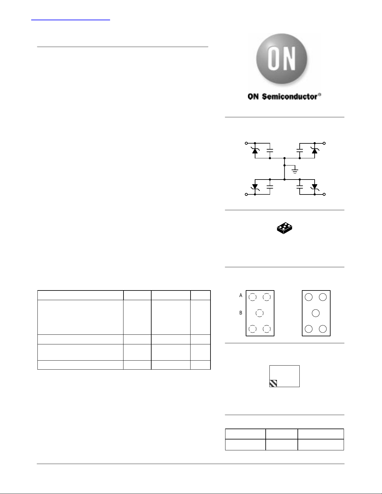
NUP4103FC
Four Channel ESD Array
This integrated transient voltage suppressor device (TVS) is
designed for applications requiring transient overvoltage protection. It
is intended for use in sensitive portable equipment and other
applications. Its integrated design provides very effective and reliable
protection for four (4) separate lines using only one package. These
devices are ideal for situations where board space is a premium.
http://onsemi.com
Features
• Unidirectional, Quad ESD Protection
• Ultra-small Flip Chip Packaging (0.95 mm x 1.33 mm)
• Compliance with IEC61000-4-2 (Level 4) Requirements
• Maximum Leakage Current of 100 nA at 3.3 V
Benefits
• Protects Four Data Lines from ESD while Reducing Component
Count
• Small Package Saves On PCB Real Estate
• Provides Protection for ESD Industry Standards, IEC 61000, HBM
and MM
• Low Leakage Capability Minimizes Power Loss in the System
Applications
• ESD Protection for Portable Equipment
• Cell Phones
• MP3 Players
• PDAs
MAXIMUM RATINGS (T
Rating Symbol Value Unit
ESD Discharge IEC61000-4-2,
- Air Discharge
- Contact Discharge
Human Body Model
Machine Model
Junction Temperature T
Operating Ambient Temperature
Range
Storage Temperature Range T
= 25°C, unless otherwise specified)
J
V
PP
J
T
A
STG
30
30
16
1.6
150 °C
-40 to +85 °C
-55 to +150 °C
kV
CIRCUIT DESCRIPTION
A1 C1
B2
A3 C3
5 PIN FLIP CHIP CSP
CASE 766AB
PLASTIC
TOP VIEW
(Bumps Down)
12 12
33
A
B
C
DEVICE MARKING
ED
BOTTOM VIEW
(Bumps Up)
A
B
C
Semiconductor Components Industries, LLC, 2003
June, 2003 - Rev. 0
E = Specific Device Code
D = Month Code
ORDERING INFORMATION
Device Package Shipping
NUP4103FCT1 Flip Chip 3000/Tape & Reel
1 Publication Order Number:
NUP4103FC/D
Page 2
NUP4103FC
ELECTRICAL CHARACTERISTICS (T
Parameter
Reverse Stand-Off Voltage V
Breakdown Voltage V
Leakage Current I
Junction Capacitance C
= 25°C unless otherwise specified)
J
Symbol Conditions Min Typ Max Unit
I
RWM
BR
R
J
= 10 A (Note 1) 5.5 V
RWM
IT = 1.0 mA (Note 2) 6.0 7.0 8.0 V
VRM = 3.3 V per line 100 nA
VR = 2.5 V, f = 1 MHz 30 pF
1. TVS devices are normally selected according to the working peak reverse voltage (V
or continuous peak operating voltage level.
is measured at pulse test current IT.
2. V
BR
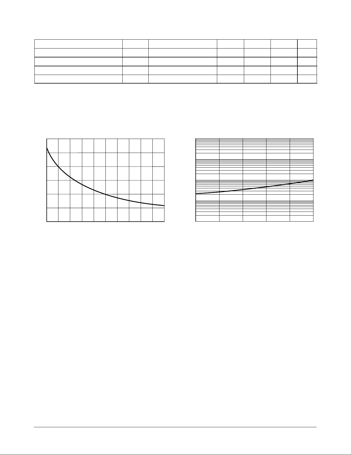
TYPICAL PERFORMANCE CURVES
(TJ = 25°C unless otherwise specified)
50
45
40
35
30
C, Capacitance (pF)
25
100.0E-9
10.0E-9
1.0E-9
, Leakage Current (A)
100.0E-12
R
I
) which should be equal or greater than the DC
RWM
20
0
12345
, Reverse Voltage (V)
V
R
Figure 1. Reverse V oltage vs Junction Capacitance
10.0E-12
-40
-15
10
35 60 85
T, Temperature (°C)
Figure 2. Reverse Leakage Current
vs Junction T emperature
http://onsemi.com
2
Page 3

NUP4103FC
2.0 V/div
Figure 3. ESD Response for Human Body Model (+8 kV)
500 mV/div
200 ns
200 ns
Figure 4. ESD Response for Human Body Model (-8 kV)
http://onsemi.com
3
Page 4

NUP4103FC
Printed Circuit Board Recommendations
500 m Pitch
Parameter
PCB Pad Size 250 m +25 / -0
Pad Shape Round
Pad Type NSMD
Solder Mask Opening 350 m ±25
Solder Stencil Thickness 125 m
Stencil Aperture 250 x 250 m sq.
Solder Flux Ratio 50/50
Solder Paste Type No Clean Type 3 or Finer
Trace Finish OSP Cu
Trace Width 150 m Max
Copper Solder Mask
300 m Solder Ball
NSMD SMD
Figure 5. Solder Mask versus Non-Solder Mask Definition
Controlled Atmosphere
TEMPERATURE (°C)
250
200
150
100
50
1 to 5 °C/s
0
225°C Min
235°C Max
183 °C
140 to 160 °C
1 to 2 min 30-100 sec
TIME (minutes)
2 to 5 °C/s
543210
Figure 6. Solder Reflow Profile
http://onsemi.com
4
Page 5

NUP4103FC
PACKAGE DIMENSIONS
5 PIN FLIP CHIP CSP
CASE 766AB-01
ISSUE O
4 X
0.10 C
TERMINAL A1
LOCATOR
0.10 C
0.05 C
5 X
C
0.03 C
b
A0.05 B
1
2
3
ABC
D1
D
A2
A
B
E
A1
A
SEATING
PLANE
NOTES:
1. DIMENSIONING AND TOLERANCING PER
ASME Y14.5M, 1994.
2. CONTROLLING DIMENSION: MILLIMETERS.
3. COPLANARITY APPLIES TO SPHERICAL
CROWNS OF SOLDER BALLS.
MILLIMETERS
DIMAMIN MAX
---
A1
A2 0.380 0.430
D 1.330 BSC
E
C
b 0.290 0.340
e 0.500 BSC
f 0.433 BSC
D1
0.680
0.210 0.270
0.960 BSC
0.866 BSC
f
e
http://onsemi.com
5
Page 6

NUP4103FC
ON Semiconductor and are registered trademarks of Semiconductor Components Industries, LLC (SCILLC). SCILLC reserves the right to make
changes without further notice to any products herein. SCILLC makes no warranty, representation or guarantee regarding the suitability of its products for any
particular purpose, nor does SCILLC assume any liability arising out of the application or use of any product or circuit, and specifically disclaims any and all
liability, including without limitation special, consequential or incidental damages. “Typical” parameters which may be provided in SCILLC data sheets and/or
specifications can and do vary in different applications and actual performance may vary over time. All operating parameters, including “Typicals” must be
validated for each customer application by customer’s technical experts. SCILLC does not convey any license under its patent rights nor the rights of others.
SCILLC products are not designed, intended, or authorized for use as components in systems intended for surgical implant into the body, or other applications
intended to support or sustain life, or for any other application in which the failure of the SCILLC product could create a situation where personal injury or death
may occur. Should Buyer purchase or use SCILLC products for any such unintended or unauthorized application, Buyer shall indemnify and hold SCILLC
and its officers, employees, subsidiaries, affiliates, and distributors harmless against all claims, costs, damages, and expenses, and reasonable attorney fees
arising out of, directly or indirectly, any claim of personal injury or death associated with such unintended or unauthorized use, even if such claim alleges that
SCILLC was negligent regarding the design or manufacture of the part. SCILLC is an Equal Opportunity/Affirmative Action Employer.
PUBLICATION ORDERING INFORMATION
Literature Fulfillment:
Literature Distribution Center for ON Semiconductor
P.O. Box 5163, Denver, Colorado 80217 USA
Phone: 303-675-2175 or 800-344-3860 Toll Free USA/Canada
Fax: 303-675-2176 or 800-344-3867 Toll Free USA/Canada
Email: ONlit@hibbertco.com
N. American Technical Support: 800-282-9855 Toll Free USA/Canada
http://onsemi.com
JAPAN: ON Semiconductor, Japan Customer Focus Center
2-9-1 Kamimeguro, Meguro-ku, Tokyo, Japan 153-0051
Phone: 81-3-5773-3850
ON Semiconductor Website: http://onsemi.com
For additional information, please contact your local
Sales Representative.
NUP4103FC/D
6
 Loading...