

Page 1

查询NUP2301MW6T1G供应商
NUP2301MW6T1
Low Capacitance Diode
Array for ESD Protection in
Two Data Lines
NUP2301MW6T1 is a MicroIntegration device designed to
provide protection for sensitive components from possible harmful
electrical transients; for example, ESD (electrostatic discharge).
Features
• Low Capacitance (2.0 pf Maximum Between I/O Lines)
• Single Package Integration Design
• Provides ESD Protection for JEDEC Standards JESD22
Machine Model = Class C
Human Body Model = Class 3B
• Protection for IEC61000−4−2 (Level 4)
8.0 kV (Contact)
15 kV (Air)
• Ensures Data Line Speed and Integrity
• Fewer Components and Less Board Space
• Direct the Transient to Either Positive Side or to the Ground
• Pb−Free Package is Available
Applications
• T1/E1 Secondary IC Protection
• T3/E3 Secondary IC Protection
• HDSL, IDSL Secondary IC Protection
• Video Line Protection
• Microcontroller Input Protection
• Base Stations
2
• I
C Bus Protection
MAXIMUM RATINGS (Each Diode) (T
Rating Symbol Value Unit
Reverse Voltage V
Forward Current I
Peak Forward Surge Current I
Repetitive Peak Reverse Voltage V
Average Rectified Forward
Current (Note 1)
(Averaged over any 20 ms Period)
Repetitive Peak Forward Current I
Non−Repetitive Peak Forward Current
t = 1.0 ms
t = 1.0 ms
t = 1.0 S
Maximum ratings are those values beyond which device damage can occur.
Maximum ratings applied to the device are individual stress limit values (not
normal operating conditions) and are not valid simultaneously. If these limits
are exceeded, device functional operation is not implied, damage may occur
and reliability may be affected.
1. FR−5 = 1.0 0.75 0.062 in.
= 25°C unless otherwise noted)
J
R
F
FM(surge)
RRM
I
F(AV)
FRM
I
FSM
70 Vdc
200 mAdc
500 mAdc
70 V
715 mA
450 mA
2.0
1.0
0.5
http://onsemi.com
PIN CONFIGURATION
AND SCHEMATIC
V
N
I/O
V
P
4
5
6
3
2
1
SC−88
CASE 419B
STYLE 23
1
2
3
MARKING DIAGRAM
68 = Specific Device Code
d
= Date Code
N/C
6
5
54I/O
N/C
d
68
ORDERING INFORMATION
Device Package Shipping
NUP2301MW6T1 SC−88 3000/Tape & Reel
NUP2301MW6T1G SC−88
(Pb−Free)
†For information on tape and reel specifications,
including part orientation and tape sizes, please
refer to our Tape and Reel Packaging Specifications
Brochure, BRD8011/D.
A
3000/Tape & Reel
†
Semiconductor Components Industries, LLC, 2005
January, 2005 − Rev. 2
1 Publication Order Number:
NUP2301MW6T1/D
Page 2
NUP2301MW6T1
THERMAL CHARACTERISTICS
Characteristic Symbol Max Unit
Thermal Resistance Junction−to−Ambient
Lead Solder Temperature Maximum 10 Seconds Duration T
Junction Temperature T
Storage Temperature T
R
q
JA
L
J
stg
625 °C/W
260 °C
−55 to +150 °C
−55 to +150 °C
ELECTRICAL CHARACTERISTICS (T
= 25°C unless otherwise noted) (Each Diode)
J
Characteristic Symbol Min Typ Max Unit
OFF CHARACTERISTICS
Reverse Breakdown Voltage (I
= 100 mA)
(BR)
Reverse Voltage Leakage Current (VR = 70 Vdc)
(VR = 25 Vdc, TJ = 150°C)
(VR = 70 Vdc, TJ = 150°C)
Capacitance (between I/O pins) (VR = 0 V, f = 1.0 MHz) C
Capacitance (between I/O pin and ground) (VR = 0 V, f = 1.0 MHz) C
Forward Voltage (IF = 1.0 mAdc)
(IF = 10 mAdc)
(IF = 50 mAdc)
(IF = 150 mAdc)
2. FR−5 = 1.0 0.75 0.062 in.
3. Alumina = 0.4 0.3 0.024 in. 99.5% alumina.
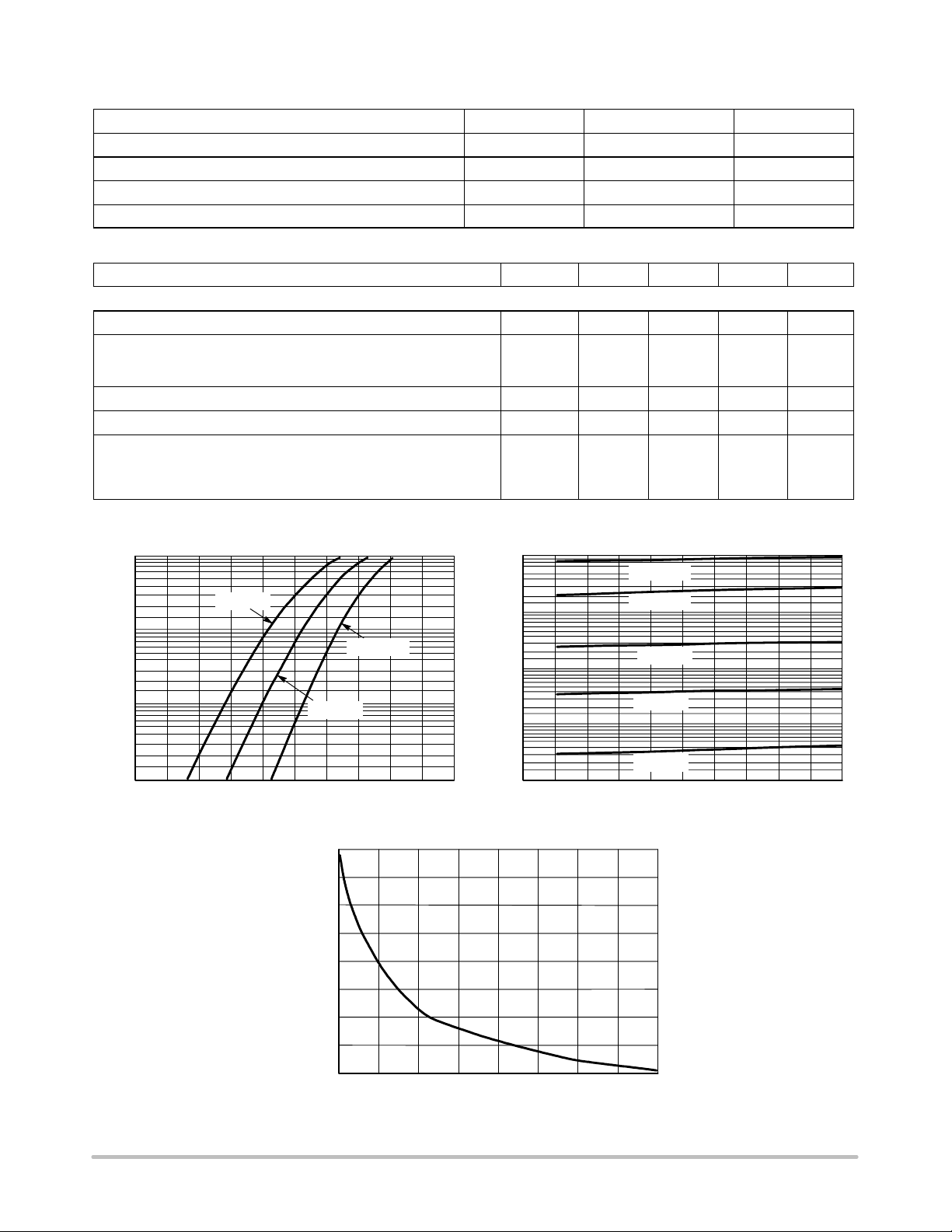
100
TA = 85°C
10
1.0
10
TA = −40°C
0.1
V
(BR)
I
R
V
70 − − Vdc
−
−
−
D
D
F
− 1.0 2.0 pF
− 1.6 3 pF
−
−
−
−
−
−
−
−
−
−
−
2.5
30
50
715
855
1000
1250
mAdc
mV
dc
TA = 150°C
TA = 125°C
TA = 85°C
1.0
, FORWARD CURRENT (mA)
F
I
0.1
0.2 0.4
Figure 1. Forward Voltage Figure 2. Leakage Current
TA = 25°C
0.6 0.8 1.0
VF, FORWARD VOLTAGE (V)
1.75
1.5
1.25
1.0
, DIODE CAPACITANCE (pF)
D
C
0.75
0
TA = 55°C
0.01
, REVERSE CURRENT (mA)
R
I
TA = 25°C
0.001
1.2
0
10 20 30 40
VR, REVERSE VOLTAGE (V)
2468
VR, REVERSE VOLTAGE (V)
Figure 3. Capacitance
50
http://onsemi.com
2
Page 3

654
S
123
NUP2301MW6T1
PACKAGE DIMENSIONS
SC−88/SC70−6/SOT−363
CASE 419B−02
ISSUE 02U
NOTES:
1. DIMENSIONING AND TOLERANCING PER ANSI
Y14.5M, 1982.
A
G
−B−
D 6 PL
MM
B0.2 (0.008)
N
J
C
2. CONTROLLING DIMENSION: INCH.
3. 419B−01 OBSOLETE, NEW STANDARD 419B−02.
INCHES
DIMAMIN MAX MIN MAX
B 1.15 1.350.045 0.053
C 0.80 1.100.031 0.043
D 0.10 0.300.004 0.012
G 0.65 BSC0.026 BSC
H −−− 0.10−−−0.004
J 0.10 0.250.004 0.010
K 0.10 0.300.004 0.012
N 0.20 REF0.008 REF
S 2.00 2.200.079 0.087
MILLIMETERS
1.80 2.200.071 0.087
H
K
SOLDERING FOOTPRINT*
0.50
0.0197
0.65
0.025
0.65
ǒ
inches
0.025
mm
Ǔ
0.40
0.0157
1.9
0.0748
SCALE 20:1
*For additional information on our Pb−Free strategy and soldering
details, please download the ON Semiconductor Soldering and
Mounting Techniques Reference Manual, SOLDERRM/D.
http://onsemi.com
3
Page 4

NUP2301MW6T1
MicroIntegration is a trademarks of Semiconductor Components Industries, LLC (SCILLC).
ON Semiconductor and are registered trademarks of Semiconductor Components Industries, LLC (SCILLC). SCILLC reserves the right to make changes without further notice
to any products herein. SCILLC makes no warranty, representation or guarantee regarding the suitability of its products for any particular purpose, nor does SCILLC assume any liability
arising out of the application or use of any product or circuit, and specifically disclaims any and all liability, including without limitation special, consequential or incidental damages.
“Typical” parameters which may be provided in SCILLC data sheets and/or specifications can and do vary in different applications and actual performance may vary over time. All
operating parameters, including “Typicals” must be validated for each customer application by customer’s technical experts. SCILLC does not convey any license under its patent rights
nor the rights of others. SCILLC products are not designed, intended, or authorized for use as components in systems intended for surgical implant into the body, or other applications
intended to support or sustain life, or for any other application in which the failure of the SCILLC product could create a situation where personal injury or death may occur. Should
Buyer purchase or use SCILLC products for any such unintended or unauthorized application, Buyer shall indemnify and hold SCILLC and its officers, employees, subsidiaries, affiliates,
and distributors harmless against all claims, costs, damages, and expenses, and reasonable attorney fees arising out of, directly or indirectly, any claim of personal injury or death
associated with such unintended or unauthorized use, even if such claim alleges that SCILLC was negligent regarding the design or manufacture of the part. SCILLC is an Equal
Opportunity/Affirmative Action Employer. This literature is subject to all applicable copyright laws and is not for resale in any manner.
PUBLICATION ORDERING INFORMATION
LITERATURE FULFILLMENT:
Literature Distribution Center for ON Semiconductor
P.O. Box 61312, Phoenix, Arizona 85082−1312 USA
Phone: 480−829−7710 or 800−344−3860 Toll Free USA/Canada
Fax: 480−829−7709 or 800−344−3867 Toll Free USA/Canada
Email: orderlit@onsemi.com
N. American Technical Support: 800−282−9855 Toll Free
USA/Canada
Japan: ON Semiconductor, Japan Customer Focus Center
2−9−1 Kamimeguro, Meguro−ku, Tokyo, Japan 153−0051
Phone: 81−3−5773−3850
http://onsemi.com
ON Semiconductor Website: http://onsemi.com
Order Literature: http://www.onsemi.com/litorder
For additional information, please contact your
local Sales Representative.
NUP2301MW6T1/D
4
Page 5

Copyright © Each Manufacturing Company.
All Datasheets cannot be modified without permission.
This datasheet has been download from :
www.AllDataSheet.com
100% Free DataSheet Search Site.
Free Download.
No Register.
Fast Search System.
www.AllDataSheet.com
 Loading...