

Page 1
查询NUP2201MR6供应商
NUP2201MR6
Low Capacitance TSOP−6
Diode−TVS Array for High
Speed Data Lines
Protection
The NUP2201MR6 transient voltage suppressor is designed to
protect high speed data lines from ESD, EFT, and lighting.
Features:
• Low Capacitance (3 pF Maximum Between I/O Lines)
• ESD Rating of Class 3B (Exceeding 8 kV) per Human Body model
and Class C (Exceeding 400 V) per Machine Model
• Protection for the Following IEC Standards:
IEC 61000−4−2 (ESD) 15 kV (air) 8 kV (contact)
IEC 61000−4−4 (EFT) 40 A (5/50 ns)
IEC 61000−4−5 (lighting) 23 A (8/20 s)
• UL Flammability Rating of 94 V−0
T ypical Applications:
• High Speed Communication Line Protection
• USB 1.1 and 2.0 Power and Data Line Protection
• Digital Video Interface (DVI)
• Monitors and Flat Panel Displays
• Pb−Free Package May be Available. The G−Suffix Denotes a
Pb−Free Lead Finish
MAXIMUM RATINGS (T
Rating
Peak Power Dissipation
8 x 20 S @ T
Operating Junction Temperature Range T
Storage Temperature Range T
Lead Solder Temperature −
Maximum (10 Seconds)
Human Body Model (HBM)
Machine Model (MM)
IEC 61000−4−2 Air (ESD)
IEC 61000−4−2 Contact (ESD)
1. Non−repetitive current pulse per Figure 1 (Pin 5 to Pin 2)
= 25°C (Note 1)
A
= 25°C unless otherwise noted)
J
Symbol Value Unit
P
pk
J
stg
T
L
ESD 16000
500 W
−40 to +125 °C
−55 to +150 °C
235 °C
V
400
20000
20000
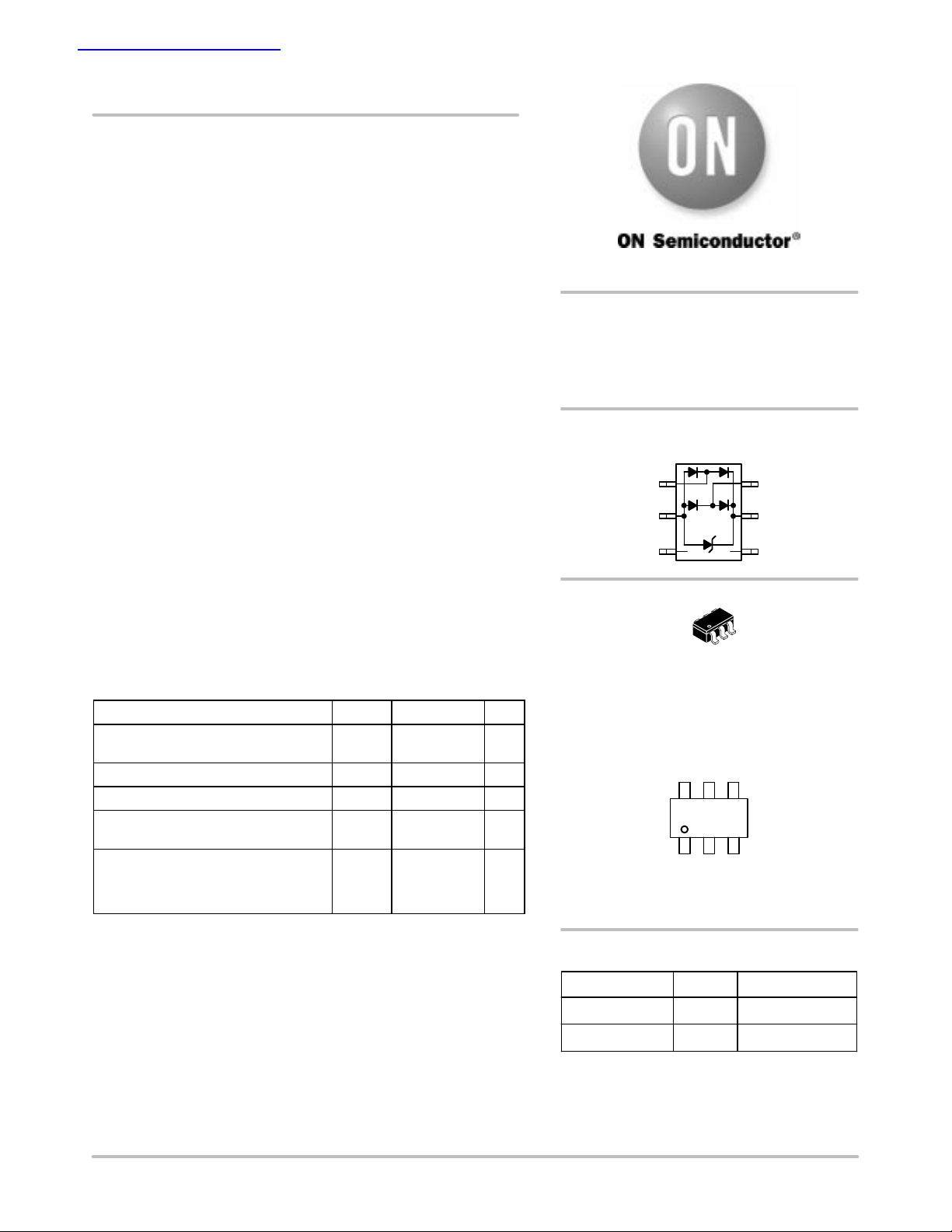
http://onsemi.com
TSOP−6 LOW CAPACITANCE
DIODE TVS ARRAY
500 WATTS PEAK POWER
6 VOLTS
PIN CONFIGURATION
AND SCHEMATIC
I/O 1
V
2
N
N/C 3
6
TSOP−6
CASE 318G
PLASTIC
MARKING DIAGRAM
M
62
62 = Specific Device Code
M
= Date Code
6 I/O
5 V
P
4 N/C
1
Semiconductor Components Industries, LLC, 2003
November, 2003 − Rev. 1
ORDERING INFORMATION
Device Package Shipping
NUP2201MR6T1 TSOP−6 3000/Tape & Reel
NUP2201MR6T1G TSOP−6 3000/Tape & Reel
†For information on tape and reel specifications,
including part orientation and tape sizes, please
refer to our Tape and Reel Packaging Specifications
Brochure, BRD8011/D.
1 Publication Order Number:
NUP2201MR6/D
†
Page 2
NUP2201MR6
ELECTRICAL CHARACTERISTICS (T
Parameter
Reverse Working Voltage V
Breakdown Voltage V
Reverse Leakage Current I
Clamping Voltage V
Clamping Voltage V
Maximum Peak Pulse Current I
Junction Capacitance C
Junction Capacitance C
Symbol Conditions Min Typ Max Unit
=25°C unless otherwise specified)
J
RWM
(Note 2) 5.0 V
IT=1 mA, (Note 3) 6.0 V
BR
V
R
C
C
PP
J
J
= 5 V 5.0 A
RWM
IPP = 5 A (Note 4) 12.5 V
IPP = 8 A (Note 4) 20 V
8x20 s Waveform 25 A
VR = 0 V, f=1 MHz between I/O Pins and GND 3.0 5.0 pF
VR = 0 V, f=1 MHz between I/O Pins 1.5 3.0 pF
2. TVS devices are normally selected according to the working peak reverse voltage (V
or continuous peak operating voltage level.
is measured at pulse test current IT.
3. V
BR
4. Non−repetitive current pulse per Figure 1 (Pin 5 to Pin 2)
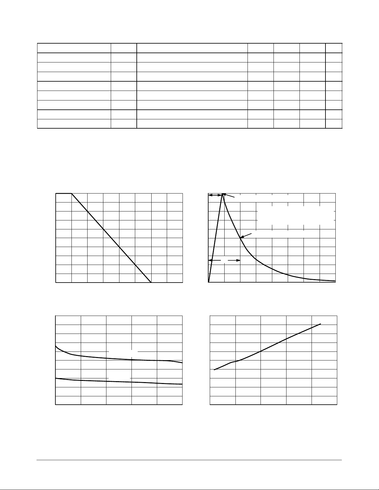
TYPICAL PERFORMANCE CURVES
(TJ = 25°C unless otherwise noted)
100
90
80
70
60
50
40
30
20
PEAK POWER DISSIPATION (%)
10
0
0 25 50 75 100 125 150 175 200
, AMBIENT TEMPERATURE (°C)
T
A
Figure 1. Pulse Derating Curve
100
t
r
90
80
70
60
50
40
30
20
% OF PEAK PULSE CURRENT
10
0
0204060
Figure 2. 8 × 20 s Pulse Waveform
), which should be equal or greater than the DC
RWM
PEAK VALUE I
RSM
@ 8 s
PULSE WIDTH (tP) IS DEFINED
AS THAT POINT WHERE THE
PEAK CURRENT DECAY = 8 s
HALF VALUE I
t
P
/2 @ 20 s
RSM
t, TIME (s)
80
5.0
4.5
4.0
3.5
3.0
I/O−Ground
2.5
2.0
1.5
I/O lines
1.0
JUNCTION CAPACITANCE (pF)
0.5
0.0
01
V
2345
, REVERSE VOLTAGE (V)
BR
Figure 3. Junction Capacitance vs Reverse V oltage
http://onsemi.com
20
18
16
14
12
10
8
6
4
CLAMPING VOLTAGE (V)
2
0
010
20 30 40 50
PEAK PULSE CURRENT (A)
Figure 4. Clamping Voltage vs. Peak Pulse Current
(8 x 20 s Waveform)
2
Page 3

NUP2201MR6
PACKAGE DIMENSIONS
TSOP−6
CASE 318G−02
ISSUE K
NOTES:
1. DIMENSIONING AND TOLERANCING PER
A
L
456
S
1
23
B
ANSI Y14.5M, 1982.
2. CONTROLLING DIMENSION: MILLIMETER.
3. MAXIMUM LEAD THICKNESS INCLUDES
LEAD FINISH THICKNESS. MINIMUM LEAD
THICKNESS IS THE MINIMUM THICKNESS
OF BASE MATERIAL.
4. DIMENSIONS A AND B DO NOT INCLUDE
MOLD FLASH, PROTRUSIONS, OR GATE
BURRS.
0.05 (0.002)
D
G
M
C
H
K
J
DIM MIN MAX MIN MAX
A 0.1142 0.12202.90 3.10
B 0.0512 0.06691.30 1.70
C 0.0354 0.04330.90 1.10
D 0.0098 0.01970.25 0.50
G 0.0335 0.04130.85 1.05
H 0.0005 0.00400.013 0.100
J 0.0040 0.01020.10 0.26
K 0.0079 0.02360.20 0.60
L 0.0493 0.06101.25 1.55
M 0 10 0 10
____
S 0.0985 0.11812.50 3.00
INCHESMILLIMETERS
SOLDERING FOOTPRINT*
2.4
0.094
0.95
0.037
1.9
0.075
0.95
0.037
0.7
0.028
1.0
0.039
Figure 5. TSOP−6
*For additional information on our Pb−Free strategy and soldering
details, please download the ON Semiconductor Soldering and
Mounting Techniques Reference Manual, SOLDERRM/D.
http://onsemi.com
3
Page 4

NUP2201MR6
ON Semiconductor and are registered trademarks of Semiconductor Components Industries, LLC (SCILLC). SCILLC reserves the right to make changes without further notice
to any products herein. SCILLC makes no warranty, representation or guarantee regarding the suitability of its products for any particular purpose, nor does SCILLC assume any liability
arising out of the application or use of any product or circuit, and specifically disclaims any and all liability, including without limitation special, consequential or incidental damages.
“Typical” parameters which may be provided in SCILLC data sheets and/or specifications can and do vary in different applications and actual performance may vary over time. All
operating parameters, including “Typicals” must be validated for each customer application by customer’s technical experts. SCILLC does not convey any license under its patent rights
nor the rights of others. SCILLC products are not designed, intended, or authorized for use as components in systems intended for surgical implant into the body, or other applications
intended to support or sustain life, or for any other application in which the failure of the SCILLC product could create a situation where personal injury or death may occur. Should
Buyer purchase or use SCILLC products for any such unintended or unauthorized application, Buyer shall indemnify and hold SCILLC and its officers, employees, subsidiaries, affiliates,
and distributors harmless against all claims, costs, damages, and expenses, and reasonable attorney fees arising out of, directly or indirectly, any claim of personal injury or death
associated with such unintended or unauthorized use, even if such claim alleges that SCILLC was negligent regarding the design or manufacture of the part. SCILLC is an Equal
Opportunity/Affirmative Action Employer. This literature is subject to all applicable copyright laws and is not for resale in any manner.
PUBLICATION ORDERING INFORMATION
LITERATURE FULFILLMENT:
Literature Distribution Center for ON Semiconductor
P.O. Box 5163, Denver, Colorado 80217 USA
Phone: 303−675−2175 or 800−344−3860 Toll Free USA/Canada
Fax: 303−675−2176 or 800−344−3867 Toll Free USA/Canada
Email: orderlit@onsemi.com
N. American Technical Support: 800−282−9855 Toll Free
USA/Canada
Japan: ON Semiconductor, Japan Customer Focus Center
2−9−1 Kamimeguro, Meguro−ku, Tokyo, Japan 153−0051
Phone: 81−3−5773−3850
http://onsemi.com
ON Semiconductor Website: http://onsemi.com
Order Literature: http://www.onsemi.com/litorder
For additional information, please contact your
local Sales Representative.
NUP2201MR6/D
4
 Loading...