

查询NTR1P02LT1供应商
NTR1P02LT1
Power MOSFET
−20 V, −1.3 A, P−Channel
SOT−23 Package
These miniature surface mount MOSFETs low R
DS(on)
assure
minimal power loss and conserve energy, making these devices ideal
for use in space sensitive power management circuitry. Typical
applications are dc−dc converters and power management in portable
and battery−powered products such as computers, printers, PCMCIA
cards, cellular and cordless telephones.
Features
• Low R
Provides Higher Efficiency and Extends Battery Life
DS(on)
• Miniature SOT−23 Surface Mount Package Saves Board Space
• Pb−Free Package is Available
MAXIMUM RATINGS (T
Drain−to−Source Voltage V
Gate−to−Source Voltage − Continuous V
Drain Current
− Continuous @ T
− Pulsed Drain Current (t
Total Power Dissipation @ TA = 25°C P
Operating and Storage Temperature Range TJ, T
Thermal Resistance − Junction−to−Ambient R
Maximum Lead Temperature for Soldering
Purposes, (1/8″ from case for 10 s)
Maximum ratings are those values beyond which device damage can occur.
Maximum ratings applied to the device are individual stress limit values (not
normal operating conditions) and are not valid simultaneously. If these limits
are exceeded, device functional operation is not implied, damage may occur
and reliability may be affected.
= 25°C unless otherwise noted)
J
Rating
= 25°C
A
≤ 10 s)
p
Symbol Value Unit
stg
−20 V
±12 V
−1.3
−4.0
400 mW
− 55 to
150
300 °C/W
260 °C
A
A
°C
DSS
I
I
DM
T
GS
D
D
JA
L
http://onsemi.com
R
(BR)DSS
−20 V 220 m
DS(on)
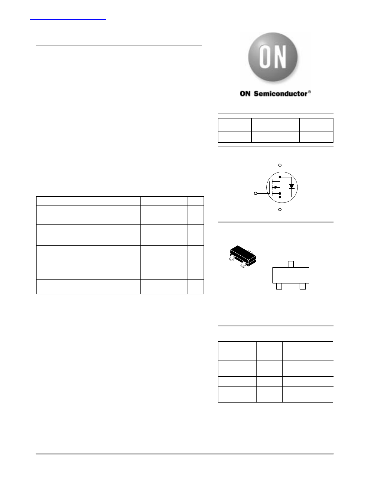
P−Channel
G
MARKING DIAGRAM/
PIN ASSIGNMENT
3
1
2
SOT−23
CASE 318
STYLE 21
Gate2Source
PO2 = Specific Device Code
W = Work Week
MAX
D
S
PO2W
1
3
Drain
ID MAXV
−1.3 A
Semiconductor Components Industries, LLC, 2004
July, 2004 − Rev. 5
ORDERING INFORMATION
Device Package Shipping
NTR1P02L T1 SOT−23 3000 Tape & Reel
NTR1P02LT1G SOT−23
(Pb−Free)
NTR1P02L T3 SOT−23 10,000 Tape & Reel
NTR1P02LT3G SOT−23
(Pb−Free)
†For information on tape and reel specifications,
including part orientation and tape sizes, please
refer to our Tape and Reel Packaging Specifications
Brochure, BRD8011/D.
1 Publication Order Number:
3000 Tape & Reel
10,000 Tape & Reel
NTR1P02LT1/D
†
NTR1P02LT1
(V
DD
0 V, I
D
)
dIS/dt = 100 A/s)
ELECTRICAL CHARACTERISTICS (T
= 25°C unless otherwise noted)
A
Characteristic Symbol Min Typ Max Unit
OFF CHARACTERISTICS
Drain−to−Source Breakdown Voltage
= 0 V, ID = −10 A)
(V
GS
Zero Gate Voltage Drain Current
(VDS = −16 V, VGS = 0 V)
(V
= −16 V, VGS = 0 V, TJ = 125°C)
DS
Gate−Body Leakage Current (VGS = ± 12 V, VDS = 0 V) I
ON CHARACTERISTICS (Note 1)
Gate Threshold Voltage
(V
= VGS, ID = −250 A)
DS
Static Drain−to−Source On−Resistance
(V
= −4.5 V, ID = −0.75 A)
GS
= −2.5 V, ID = −0.5 A)
(V
GS
DYNAMIC CHARACTERISTICS
Input Capacitance
(VDS = −5.0 V) C
Output Capacitance (VDS = −5.0 V) C
Transfer Capacitance (VDG = −5.0 V) C
SWITCHING CHARACTERISTICS (Note 2)
Turn−On Delay Time
Rise Time
Turn−Off Delay Time
(VDD = −5.0 V, ID = −1.0 A,
= −5.
= −1.0 A,
RL = 5.0 , RG = 6.0 )
Fall Time t
Total Gate Charge (VDS = −16 V, ID = −1.5 A,
VGS = −4.0 V)
SOURCE−DRAIN DIODE CHARACTERISTICS
Continuous Current
Pulsed Current I
Forward Voltage (Note 2) (VGS = 0 V, IS = −0.6 A) V
Reverse Recovery Time
(IS = −1.0 A, VGS = 0 V,
dI
/dt = 100 A/s
Reverse Recovery Stored Charge Q
1. Pulse Test: Pulse Width ≤300 s, Duty Cycle ≤ 2%.
2. Switching characteristics are independent of operating junction temperature.
V
(BR)DSS
I
DSS
GSS
V
GS(th)
r
DS(on)
t
d(on)
t
d(off)
Q
I
SM
t
t
t
iss
oss
rss
t
S
SD
rr
a
b
RR
−20 V
A
−1.0
−10
±100 nA
−0.7 −1.0 −1.25 V
0.135
0.190
225
0.22
0.35
pF
130
55
7.0
r
15
ns
18
f
T
20
5500 pC
−0.6 A
−0.75
−1.0 V
16
ns
11
5.5
0.0085 C
http://onsemi.com
2

NTR1P02LT1
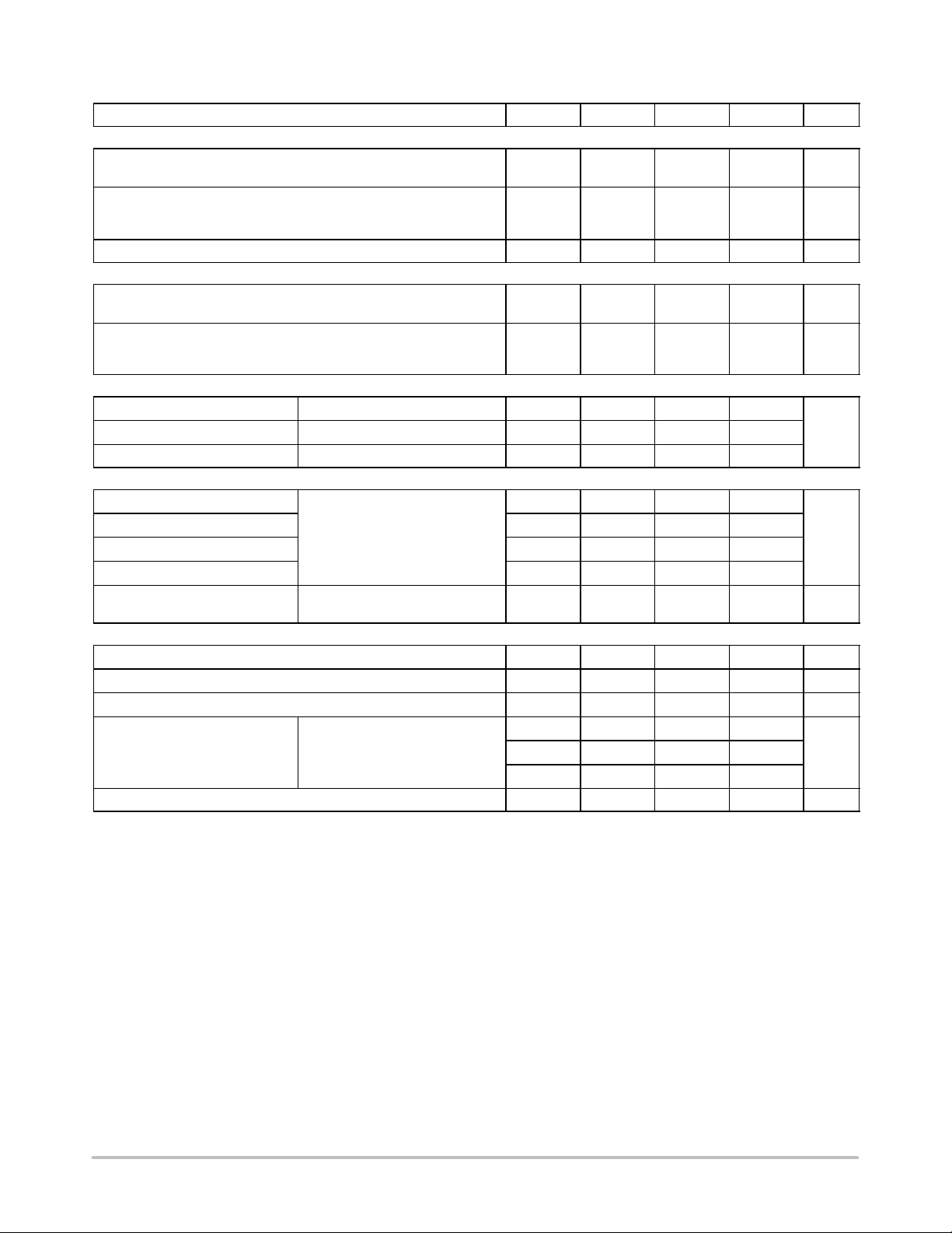
2.5
2
VGS = −3 V
−2.8 V
−2.6 V
1.5
−2.4 V
−2.2 V
1
, DRAIN CURRENT (AMPS)
0.5
D
−I
0
0
−V
, DRAIN−TO−SOURCE VOLTAGE (VOLTS)
DS
Figure 1. On−Region Characteristics Figure 2. Transfer Characteristics
0.04
ID = −10 A
T
= 25°C
0.03
0.02
J
21
−1.2 V
−2 V
3
1.4
VDS ≥ −10 V
TJ = 25°C
1.2
1
−1.8 V
0.8
−1.6 V
0.6
0.4
, DRAIN CURRENT (AMPS)
−1.4 V
4 1.6 1.8 2 2.2
D
−I
0.2
0
5
1 2.41.41.2
TJ = 25°C
TJ = 100°C
TJ = −55°C
−VGS, GATE−TO−SOURCE VOLTAGE (VOLTS)
0.3
TJ = 25°C
V
= −2.5 V
0.25
0.2
0.15
GS
TJ = 100°C
TJ = 25°C
0.01
, DRAIN−TO−SOURCE RESISTANCE ()
0
DS(on)
0
R
42
−VGS, GATE−TO−SOURCE VOLTAGE (VOLTS) −ID, DRAIN CURRENT (AMPS)
Figure 3. On−Resistance versus
Gate−to−Source V oltage
0.3
ID = −0.5 A
V
= −2.5 V
GS
0.2
0.1
(NORMALIZED)
, DRAIN−TO−SOURCE RESISTANCE
0
DS(on)
R
−50 50250−25 75 125100
TJ, JUNCTION TEMPERATURE (°C) −VDS, DRAIN−TO−SOURCE VOLTAGE (VOLTS)
0.1
0.05
, DRAIN−TO−SOURCE RESISTANCE ()
0
610
8 0.9
0.2 0.50.40.3 0.6 0.7 10.8
DS(on)
R
Figure 4. On−Resistance versus Drain Current
1000
VGS = 0 V
100
10
, LEAKAGE (nA)
1
DSS
−I
0.1
0.01
150
412816
TJ = −55°C
and Gate Voltage
TJ = 125°C
TJ = 100°C
TJ = 25°C
Figure 5. On−Resistance Variation with
Temperature
http://onsemi.com
Figure 6. Drain−to−Source Leakage Current
versus V oltage
3

NTR1P02LT1
5000
4500
4000
3500
VDS = 0V
VGS = 0V
T
= 25°C
J
6
Q
4
T
3000
DS
10
C
iss
Q
2
C
oss
C
rss
1550
, GATE−TO−SOURCE VOLTAGE (VOLTS)
GS
0
−V
25 0 21
1
Q
2
VDS = −16 V
I
= −1.5 A
D
= 25°C
T
J
34
QG, TOTAL GATE CHARGE (nC)
2500
2000
1500
C, CAPACITANCE (pF)
1000
500
0
15
10 20
5
−V
GS
−V
GATE−TO−SOURCE OR DRAIN−TO−SOURCE VOLTAGE (VOLTS)
Figure 7. Capacitance Variation Figure 8. Gate−to−Source and
Drain−to−Source Voltage versus Total Charge
100
VDD = −16 V
I
= −1 A
D
t
r
t
f
10
t
d(off)
t, TIME (ns)
1
t
d(on)
1 10 100 1.00E−01 5.00E−013.00E−01 7.00E−01 9.00E−01
RG, GATE RESISTANCE ()−V
Figure 9. Resistive Switching Time Variation
versus Gate Resistance
0.8
VGS = 0 V
T
= 25°C
J
0.6
0.4
0.2
, SOURCE CURRENT (AMPS)
S
−I
0
, SOURCE−TO−DRAIN VOLTAGE (VOLTS)
SD
Figure 10. Diode Forward Voltage versus
Current
28
24
20
16
12
8
4
0
http://onsemi.com
4
NTR1P02LT1
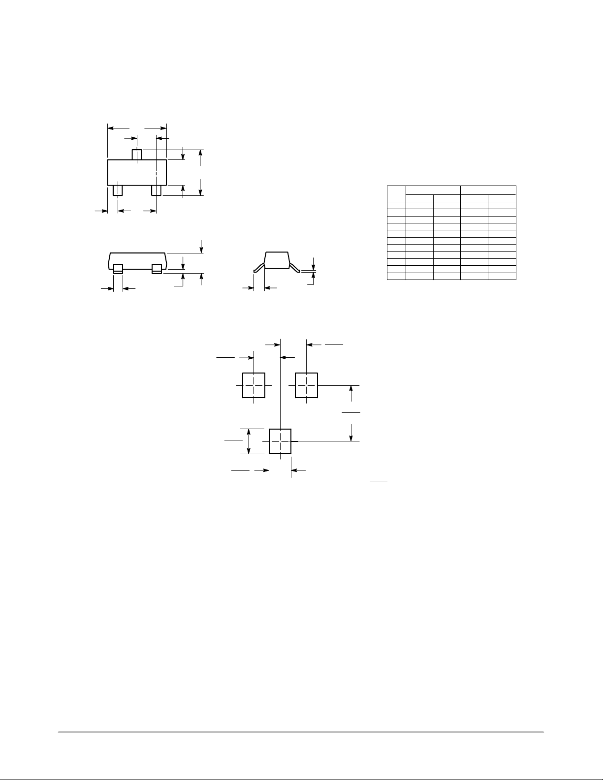
PACKAGE DIMENSIONS
SOT−23 (TO−236)
CASE 318−09
ISSUE AJ
NOTES:
A
L
3
1
V
G
BS
2
C
D
H
J
K
SOLDERING FOOTPRINT*
0.95
0.95
0.037
0.037
1. DIMENSIONING AND TOLERANCING PER ANSI
Y14.5M, 1982.
2. CONTROLLING DIMENSION: INCH.
3. MAXIUMUM LEAD THICKNESS INCLUDES LEAD
FINISH THICKNESS. MINIMUM LEAD
THICKNESS IS THE MINIMUM THICKNESS OF
BASE MATERIAL.
4. 318−01, −02, AND −06 OBSOLETE, NEW
STANDARD 318−09.
DIMAMIN MAX MIN MAX
STYLE 21:
INCHES
0.1102 0.1197 2.80 3.04
B 0.0472 0.0551 1.20 1.40
C 0.0385 0.0498 0.99 1.26
D 0.0140 0.0200 0.36 0.50
G 0.0670 0.0826 1.70 2.10
H 0.0040 0.0098 0.10 0.25
J 0.0034 0.0070 0.085 0.177
K 0.0180 0.0236 0.45 0.60
L 0.0350 0.0401 0.89 1.02
S 0.0830 0.0984 2.10 2.50
V 0.0177 0.0236 0.45 0.60
PIN 1. GATE
2. SOURCE
3. DRAIN
MILLIMETERS
2.0
0.079
0.9
0.035
0.8
0.031
SCALE 10:1
inches
mm
*For additional information on our Pb−Free strategy and soldering
details, please download the ON Semiconductor Soldering and
Mounting Techniques Reference Manual, SOLDERRM/D.
http://onsemi.com
5

NTR1P02LT1
ON Semiconductor and are registered trademarks of Semiconductor Components Industries, LLC (SCILLC). SCILLC reserves the right to make changes without further notice
to any products herein. SCILLC makes no warranty, representation or guarantee regarding the suitability of its products for any particular purpose, nor does SCILLC assume any liability
arising out of the application or use of any product or circuit, and specifically disclaims any and all liability, including without limitation special, consequential or incidental damages.
“Typical” parameters which may be provided in SCILLC data sheets and/or specifications can and do vary in different applications and actual performance may vary over time. All
operating parameters, including “Typicals” must be validated for each customer application by customer’s technical experts. SCILLC does not convey any license under its patent rights
nor the rights of others. SCILLC products are not designed, intended, or authorized for use as components in systems intended for surgical implant into the body, or other applications
intended to support or sustain life, or for any other application in which the failure of the SCILLC product could create a situation where personal injury or death may occur. Should
Buyer purchase or use SCILLC products for any such unintended or unauthorized application, Buyer shall indemnify and hold SCILLC and its officers, employees, subsidiaries, affiliates,
and distributors harmless against all claims, costs, damages, and expenses, and reasonable attorney fees arising out of, directly or indirectly, any claim of personal injury or death
associated with such unintended or unauthorized use, even if such claim alleges that SCILLC was negligent regarding the design or manufacture of the part. SCILLC is an Equal
Opportunity/Affirmative Action Employer. This literature is subject to all applicable copyright laws and is not for resale in any manner.
PUBLICATION ORDERING INFORMATION
LITERATURE FULFILLMENT:
Literature Distribution Center for ON Semiconductor
P.O. Box 61312, Phoenix, Arizona 85082−1312 USA
Phone: 480−829−7710 or 800−344−3860 Toll Free USA/Canada
Fax: 480−829−7709 or 800−344−3867 Toll Free USA/Canada
Email: orderlit@onsemi.com
N. American Technical Support: 800−282−9855 Toll Free
USA/Canada
Japan: ON Semiconductor, Japan Customer Focus Center
2−9−1 Kamimeguro, Meguro−ku, Tokyo, Japan 153−0051
Phone: 81−3−5773−3850
http://onsemi.com
ON Semiconductor Website: http://onsemi.com
Order Literature: http://www.onsemi.com/litorder
For additional information, please contact your
local Sales Representative.
NTR1P02LT1/D
6
 Loading...