

NTMFS6H818N
MOSFET – Power, Single,
N-Channel
80 V, 3.7 mW, 123 A
Features
• Small Footprint (5x6 mm) for Compact Design
• Low R
• Low Q
to Minimize Conduction Losses
DS(on)
and Capacitance to Minimize Driver Losses
G
• These Devices are Pb−Free and are RoHS Compliant
MAXIMUM RATINGS (T
Parameter
Drain−to−Source Voltage V
Gate−to−Source Voltage V
Continuous Drain
Current R
(Notes 1, 3)
Power Dissipation
R
JC
Continuous Drain
Current R
(Notes 1, 2, 3)
Power Dissipation
R
JA
Pulsed Drain Current
Operating Junction and Storage Temperature TJ, T
Source Current (Body Diode) I
Single Pulse Drain−to−Source Avalanche
Energy (I
Lead Temperature for Soldering Purposes
(1/8″ from case for 10 s)
Stresses exceeding those listed in the Maximum Ratings table may damage the
device. If any of these limits are exceeded, device functionality should not be
assumed, damage may occur and reliability may be affected.
JC
(Note 1)
JA
(Notes 1 & 2)
= 9.3 A)
L(pk)
THERMAL RESISTANCE MAXIMUM RATINGS
Parameter Symbol Value Unit
Junction−to−Case − Steady State
Junction−to−Ambient − Steady State (Note 2)
1. The entire application environment impacts the thermal resistance values shown,
they are not constants and are only valid for the particular conditions noted.
2. Surface−mounted on FR4 board using a 650 mm
3. Maximum current for pulses as long as 1 second is higher but is dependent
on pulse duration and duty cycle.
= 25°C unless otherwise noted)
J
Symbol Value Unit
TC = 25°C
Steady
State
Steady
State
TA = 25°C, t
TC = 100°C 87
TC = 25°C
TC = 100°C 68
TA = 25°C
TA = 100°C 14
TA = 25°C
TA = 100°C 1.9
= 10 s
p
P
P
I
E
R
R
2
, 2 oz. Cu pad.
DSS
GS
I
D
D
I
D
D
DM
S
AS
T
L
JC
JA
stg
80 V
±20 V
123
136
20
3.8
900 A
−55 to
+ 175
113 A
731 mJ
260 °C
1.1
39
A
W
A
W
°C
°C/W
www.onsemi.com
V
(BR)DSS
80 V
G (4)
R
MAX ID MAX
DS(ON)
3.7 m @ 10 V
D (5)
S (1,2,3)
N−CHANNEL MOSFET
123 A
MARKING
DIAGRAM
1
DFN5
(SO−8FL)
CASE 488AA
STYLE 1
A = Assembly Location
Y = Year
W = Work Week
ZZ = Lot Traceability
S
S
S
G
D
D
6H818N
AYWZZ
D
D
ORDERING INFORMATION
See detailed ordering, marking and shipping information in the
package dimensions section on page 5 of this data sheet.
© Semiconductor Components Industries, LLC, 2017
May, 2019 − Rev. 1
1 Publication Order Number:
NTMFS6H818N/D
NTMFS6H818N
ELECTRICAL CHARACTERISTICS (T
Parameter
= 25°C unless otherwise specified)
J
Symbol Test Condition Min Ty p Max Unit
OFF CHARACTERISTICS
Drain−to−Source Breakdown Voltage
Drain−to−Source Breakdown Voltage
V
V
Temperature Coefficient
Zero Gate Voltage Drain Current I
Gate−to−Source Leakage Current I
(BR)DSS
(BR)DSS
T
J
DSS
GSS
VGS = 0 V, ID = 250 A
/
VGS = 0 V,
V
= 80 V
DS
TJ = 25°C 10
TJ = 125°C 100
VDS = 0 V, VGS = 20 V 100 nA
80 V
39
mV/°C
A
ON CHARACTERISTICS (Note 4)
Gate Threshold Voltage
Threshold Temperature Coefficient V
V
GS(TH)/TJ
Drain−to−Source On Resistance R
Forward Transconductance g
GS(TH)
DS(on)
FS
VGS = VDS, ID = 190 A
VGS = 10 V ID = 20 A 3.1 3.7
VGS = 6 V ID = 20 A 4.6 5.7
VDS =15 V, ID = 50 A 170 S
2.0 4.0 V
7.0 mV/°C
m
CHARGES, CAPACITANCES & GATE RESISTANCE
Input Capacitance
Output Capacitance C
Reverse Transfer Capacitance C
Output Charge Q
Total Gate Charge Q
Threshold Gate Charge Q
Gate−to−Source Charge Q
Gate−to−Drain Charge Q
Plateau Voltage V
C
ISS
OSS
RSS
OSS
G(TOT)
G(TH)
GS
GD
GP
VGS = 0 V, f = 1 MHz, VDS = 40 V
VGS = 10 V, VDS = 40 V; ID = 50 A
3100
440
20
66 nC
46
9.0
15
8.0
5.0 V
pF
nC
SWITCHING CHARACTERISTICS (Note 5)
Turn−On Delay Time
t
d(ON)
Rise Time t
Turn−Off Delay Time t
d(OFF)
Fall Time t
r
f
VGS = 10 V, VDS = 64 V,
= 50 A, RG = 2.5
I
D
22
98
49
21
ns
DRAIN−SOURCE DIODE CHARACTERISTICS
Forward Diode Voltage
Reverse Recovery Time t
Charge Time t
Discharge Time t
Reverse Recovery Charge Q
V
SD
RR
a
b
RR
VGS = 0 V,
I
= 20 A
S
VGS = 0 V, dIS/dt = 100 A/s,
I
= 50 A
S
TJ = 25°C 0.8 1.2
TJ = 125°C 0.7
63
31
32
55 nC
V
ns
Product parametric performance is indicated in the Electrical Characteristics for the listed test conditions, unless otherwise noted. Product
performance may not be indicated by the Electrical Characteristics if operated under different conditions.
4. Pulse Test: pulse width v 300 s, duty cycle v 2%.
5. Switching characteristics are independent of operating junction temperatures.
www.onsemi.com
2
NTMFS6H818N
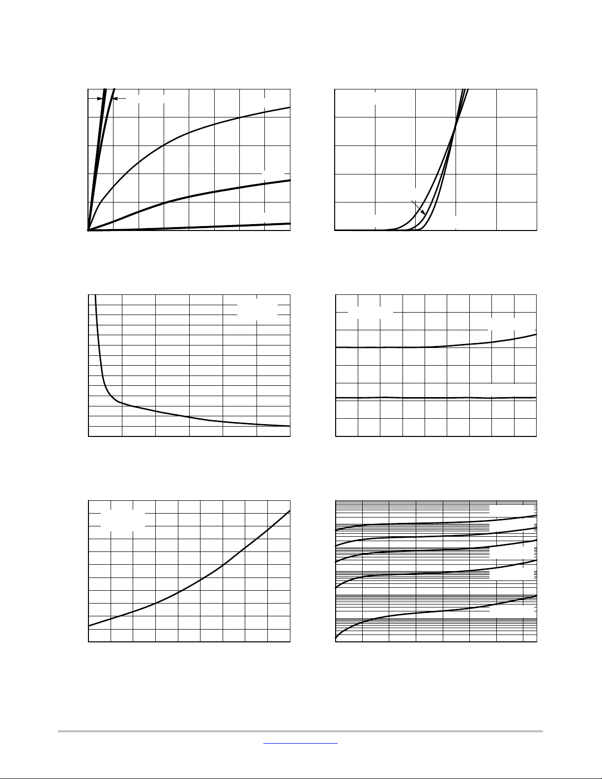
TYPICAL CHARACTERISTICS
250
5.5 to 10 V
200
150
100
, DRAIN CURRENT (A)
D
I
50
0
VDS, DRAIN−TO−SOURCE VOLTAGE (V) VGS, GATE−TO−SOURCE VOLTAGE (V)
Figure 1. On−Region Characteristics Figure 2. Transfer Characteristics
16
14
12
10
8
6
4
, DRAIN−TO−SOURCE RESISTANCE (m)
2
DS(on)
4
R
VGS, GATE−TO−SOURCE VOLTAGE (V) ID, DRAIN CURRENT (A)
Figure 3. On−Resistance vs. Gate−to−Source
3210
Voltage
250
5.0 V
4.5 V
VGS = 4.0 V
54 6
687
ID = 20 A
= 25°C
T
J
1098765
VDS = 10 V
200
150
100
, DRAIN CURRENT (A)
D
I
50
0
6.0
5.5
5.0
4.5
4.0
3.5
3.0
2.5
, DRAIN−TO−SOURCE RESISTANCE (m)
2.0
DS(on)
R
TJ = 25°C
10
TJ = 25°C
TJ = 125°C
37
TJ = −55°C
542
30 45
25 40
3515 205
VGS = 6.0 V
Figure 4. On−Resistance vs. Drain Current and
Gate Voltage
VGS = 10 V
50
2.6
2.4
ID = 20 A
= 10 V
V
2.2
2.0
1.8
1.6
1.4
1.2
1.0
0.8
0.6
0.4
, DRAIN−TO−SOURCE RESISTANCE (NORMALIZED)
DS(on)
R
GS
TJ, JUNCTION TEMPERATURE (°C) VDS, DRAIN−TO−SOURCE VOLTAGE (V)
Figure 5. On−Resistance Variation with
Temperature
150
1251007550250−25−50
175
www.onsemi.com
1M
100K
10K
1K
, LEAKAGE (nA)
100
DSS
I
10
1
3
TJ = 175°C
TJ = 150°C
TJ = 125°C
TJ = 85°C
TJ = 25°C
15 45
5535255
Figure 6. Drain−to−Source Leakage Current
vs. Voltage
7565
 Loading...