NSD914XV2T1
l
n
l
Preferred Device
High−Speed
Switching Diode
Features
• High−Speed Switching Applications
• Lead Finish: 100% Matte Sn (Tin)
• Qualified Maximum Reflow Temperature: 260°C
• Extremely Small SOD−523 Package
• Pb−Free Package is Available
http://onsemi.com
1
CATHODE
2
ANODE
MAXIMUM RATINGS (T
Reverse Voltage V
Forward Current I
Peak Forward Surge Current I
Stresses exceeding Maximum Ratings may damage the device. Maximum
Ratings are stress ratings only. Functional operation above the Recommended
Operating Conditions is not implied. Extended exposure to stresses above the
Recommended Operating Conditions may affect device reliability.
= 25°C)
A
Rating Symbol Max Unit
R
F
FM(surge)
100 V
200 mAdc
500 mAdc
THERMAL CHARACTERISTICS
Characteristic Symbol Max Unit
Total Device Dissipation FR−5 Board (Note 1)
TA = 25°C
Derate above 25°C
Thermal Resistance
Junction-to-Ambient
Junction and Storage Temperature TJ, T
1. FR−4 @ Minimum Pad.
Characteristic Symbol Min Max Unit
OFF CHARACTERISTICS
Reverse Breakdown Voltage
(IBR = 100 mAdc)
Reverse Voltage Leakage Current
(VR = 20 Vdc)
(VR = 75 Vdc)
Diode Capacitance
(VR = 0 V, f = 1.0 MHz)
Forward Voltage
(IF = 10 mAdc)
Reverse Recovery Time
(IF = IR = 10 mAdc)
P
D
R
q
JA
V
(BR)
I
R
C
D
V
F
t
rr
200
1.57mWmW/°C
635 °C/W
150 °C
stg
100 − Vdc
−−25
5.0
− 4.0 pF
− 1.0 Vdc
− 4.0 ns
nAdc
mAdc
2
1
SOD−523
CASE 502
PLASTIC
5D = Specific Device Code
M = Date Code
G = Pb−Free Package
(Note: Microdot may be in either location)
MARKING
DIAGRAM
5D MG
12
G
ORDERING INFORMATION
Device Package Shipping†
NSD914XV2T1 SOD−523 3000/Tape & Ree
NSD914XV2T1G SOD−523
(Pb−Free)
†For information on tape and reel specifications,
including part orientation and tape sizes, please
refer to our Tape and Reel Packaging Specificatio
Brochure, BRD8011/D.
Preferred devices are recommended choices for future use
and best overall value.
3000/Tape & Ree
© Semiconductor Components Industries, LLC, 2006
December, 2006 − Rev. 3
1 Publication Order Number:
NSD914XV2T1/D

+10 V
820 Ω
0.1 μF
2.0 k
100 μH
NSD914XV2T1
I
t
t
r
I
0.1 μF
F
p
10%
t
F
t
rr
t
50 Ω OUTPUT
PULSE
GENERATOR
100
10
1.0
, FORWARD CURRENT (mA)
F
I
0.1
DUT
Notes: 1. A 2.0 kΩ variable resistor adjusted for a Forward Current (IF) of 10 mA.
Notes: 2. Input pulse is adjusted so I
Notes: 3. tp » t
rr
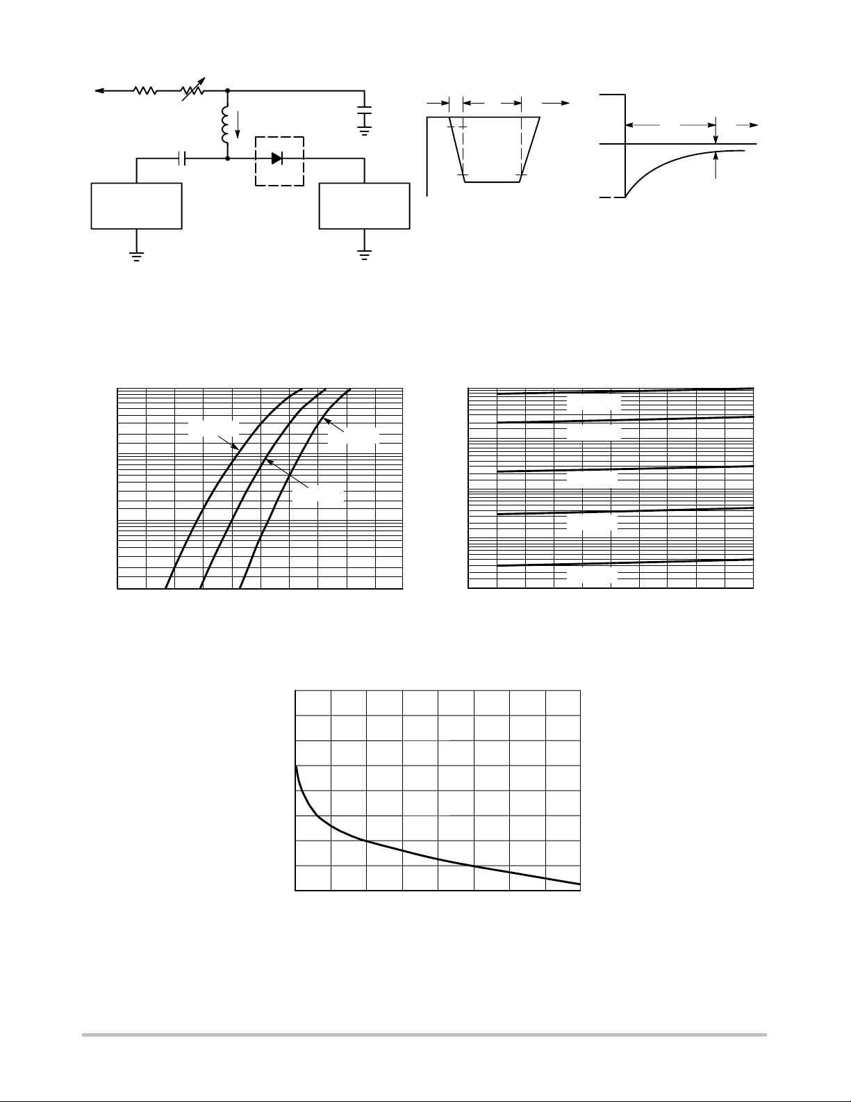
Figure 1. Recovery Time Equivalent Test Circuit
TA = 85°C
TA = 25°C
VF, FORWARD VOLTAGE (VOLTS)
50 Ω INPUT
SAMPLING
OSCILLOSCOPE
TA = −40°C
1.0 1.20.2 0.4 0.6 0.8
90%
V
R
INPUT SIGNAL
is equal to 10 mA.
R(peak)
10
1.0
m
0.1
0.01
, REVERSE CURRENT ( A)
R
I
0.001
0
i
= 1.0 mA
I
R
R(REC)
OUTPUT PULSE
(IF = IR = 10 mA; MEASURED
at i
= 1.0 mA)
R(REC)
TA = 150°C
TA = 125°C
TA = 85°C
TA = 55°C
TA = 25°C
10 20 30 40 50
VR, REVERSE VOLTAGE (VOLTS)
Figure 2. Forward Voltage
0.68
0.64
0.60
0.56
, DIODE CAPACITANCE (pF)
D
C
0.52
0
Figure 3. Leakage Current
2.0 4.0 6.0 8.0
VR, REVERSE VOLTAGE (VOLTS)
Figure 4. Capacitance
http://onsemi.com
2
 Loading...