

ON Semiconductor NJW21193G, NJW21194G Service Manual
NJW21193G (PNP)
NJW21194G (NPN)
Preferred Devices
Silicon Power Transistors
The NJW21193G and NJW21194G utilize Perforated Emitter
technology and are specifically designed for high power audio output,
disk head positioners and linear applications.
Features
•Total Harmonic Distortion Characterized
•High DC Current Gain -
hFE = 20 Min @ IC = 8 Adc
•Excellent Gain Linearity
•High SOA: 2.25 A, 80 V, 1 Second
•These are Pb-Free Devices
MAXIMUM RATINGS
Rating Symbol Value Unit
Collector-Emitter Voltage V
Collector-Base Voltage V
Emitter-Base Voltage V
Collector-Emitter Voltage - 1.5 V V
Collector Current - Continuous
Collector Current - Peak (Note 1)
Base Current - Continuous I
Total Power Dissipation @ TC = 25°C
Derate Above 25°C
Operating and Storage Junction
Temperature Range
CEO
CBO
EBO
CEX
I
P
TJ, T
C
B
D
stg
THERMAL CHARACTERISTICS
Characteristic Symbol Max Unit
Thermal Resistance,
Junction-to-Case
Thermal Resistance,
Junction-to-Ambient
Stresses exceeding Maximum Ratings may damage the device. Maximum
Ratings are stress ratings only. Functional operation above the Recommended
Operating Conditions is not implied. Extended exposure to stresses above the
Recommended Operating Conditions may affect device reliability.
1. Pulse Test: Pulse Width = 5 ms, Duty Cycle ≤ 10%.
R
q
JC
R
q
JA
250 Vdc
400 Vdc
5.0 Vdc
400 Vdc
16
30
5.0 Adc
200
1.6
-āā 65 to
+150
0.625 °C/W
40 °C/W
Adc
W
W/°C
°C
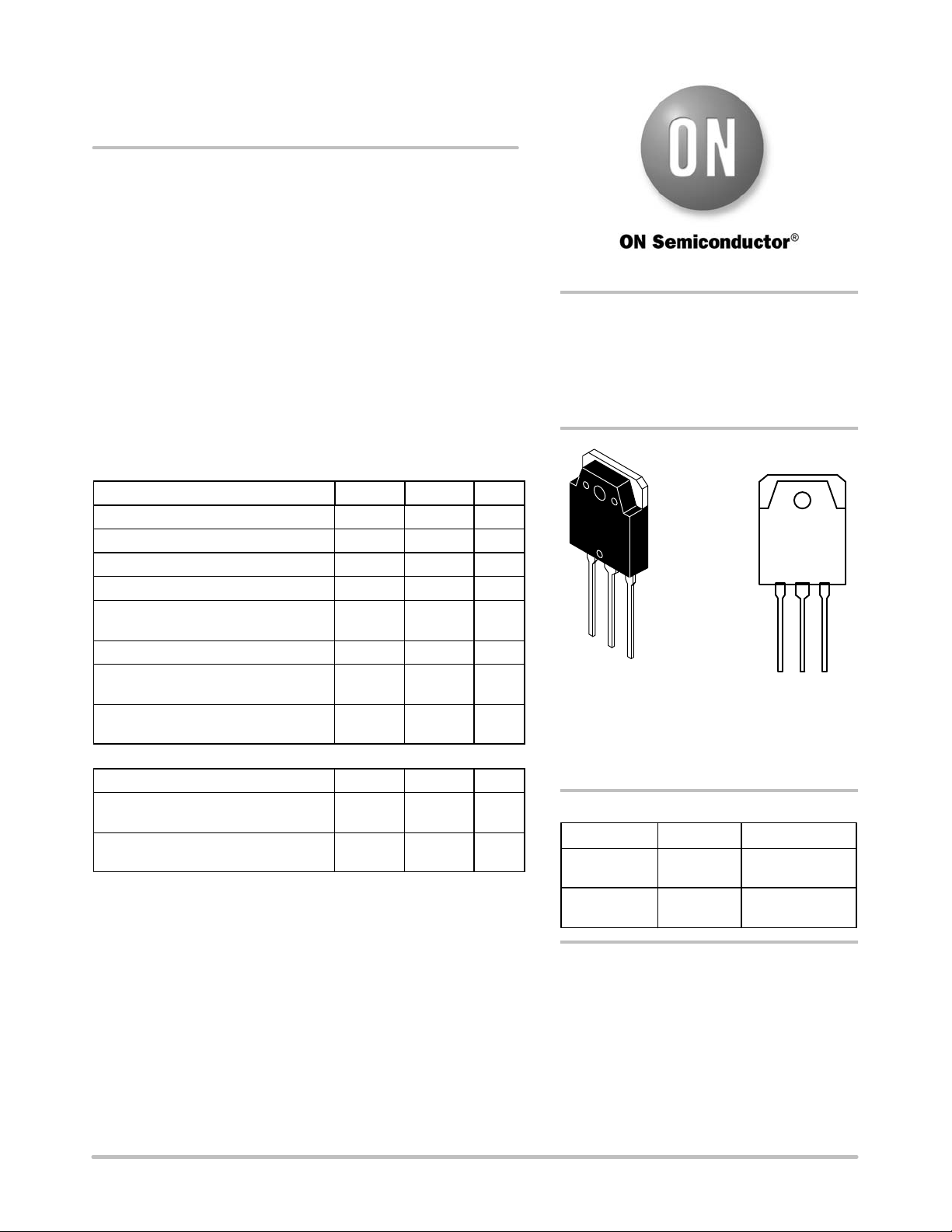
http://onsemi.com
16 AMPERES
COMPLEMENTARY SILICON
POWER TRANSISTORS
250 VOLTS, 200 WATTS
MARKING
DIAGRAM
NJW2119xG
TO-3P
CASE 340AB
x = 3 or 4
G = Pb-Free Package
A = Assembly Location
Y = Year
WW = Work Week
ORDERING INFORMATION
Device Package Shipping
NJW21193G TO-3P
(Pb-Free)
NJW21194G TO-3P
(Pb-Free)
Preferred devices are recommended choices for future use
and best overall value.
AYWW
30 Units/Rail
30 Units/Rail
© Semiconductor Components Industries, LLC, 2008
January, 2008 - Rev. 0
1 Publication Order Number:
NJW21193/D
NJW21193G (PNP) NJW21194G (NPN)
ELECTRICAL CHARACTERISTICS (T
= 25°C unless otherwise noted)
C
Characteristic
OFF CHARACTERISTICS
Collector-Emitter Sustaining Voltage
(IC = 100 mAdc, IB = 0)
Collector Cutoff Current
(VCE = 200 Vdc, IB = 0)
Emitter Cutoff Current
(VCE = 5 Vdc, IC = 0)
Collector Cutoff Current
(VCE = 250 Vdc, V
BE(off)
= 1.5 Vdc)
SECOND BREAKDOWN
Second Breakdown Collector Current with Base Forward Biased
(VCE = 50 Vdc, t = 1 s (non-repetitive)
(VCE = 80 Vdc, t = 1 s (non-repetitive)
ON CHARACTERISTICS
DC Current Gain
(IC = 8 Adc, VCE = 5 Vdc)
(IC = 16 Adc, IB = 5 Adc)
Base-Emitter On Voltage
(IC = 8 Adc, VCE = 5 Vdc)
Collector-Emitter Saturation Voltage
(IC = 8 Adc, IB = 0.8 Adc)
(IC = 16 Adc, IB = 3.2 Adc)
DYNAMIC CHARACTERISTICS
Total Harmonic Distortion at the Output
V
= 28.3 V, f = 1 kHz, P
RMS
LOAD
= 100 W
RMS
h
FE
unmatched
(Matched pair hFE = 50 @ 5 A/5 V) hFE
matched
Current Gain Bandwidth Product
(IC = 1 Adc, VCE = 10 Vdc, f
= 1 MHz)
test
Output Capacitance
(VCB = 10 Vdc, IE = 0, f
= 1 MHz)
test
Symbol Min Typ Max Unit
V
CEO(sus)
I
CEO
I
EBO
I
CEX
I
S/b
h
FE
V
BE(on)
V
CE(sat)
T
HD
f
C
T
ob
250 - - Vdc
- - 100
- - 100
- - 100
4.0
2.25
20
8
-
-
-
-
-
-
80
-
mAdc
mAdc
mAdc
- - 2.2 Vdc
-
-
-
-
-
-
0.8
0.08
1.4
4
-
-
4 - - MHz
- - 500 pF
Adc
Vdc
%
T
f, CURRENT GAIN BANDWIDTH PRODUCT (MHz)
6.5
6.0
5.5
5.0
4.5
4.0
3.5
3.0
VCE = 10 V
5 V
TJ = 25°C
f
= 1 MHz
test
PNP NJW21193G
1.0 100.1
IC COLLECTOR CURRENT (AMPS)
Figure 1. Typical Current Gain
Bandwidth Product
8.0
7.0
6.0
5.0
4.0
3.0
2.0
1.0
T
0
f, CURRENT GAIN BANDWIDTH PRODUCT (MHz)
http://onsemi.com
2
NPN NJW21194G
TJ = 25°C
f
= 1 MHz
test
1.0 100.1
IC COLLECTOR CURRENT (AMPS)
Figure 2. Typical Current Gain
Bandwidth Product
10 V
VCE = 5 V
1000
NJW21193G (PNP) NJW21194G (NPN)
TYPICAL CHARACTERISTICS
PNP NJW21193G NPN NJW21194G
1000
100
, DC CURRENT GAIN
FE
h
1000
100
, DC CURRENT GAIN
FE
h
10
TJ = 100°C
25°C
-25°C
VCE = 20 V
TJ = 100°C
25°C
-25°C
IC COLLECTOR CURRENT (AMPS)
100
, DC CURRENT GAIN
FE
h
VCE = 20 V
100101.00.1
10
IC COLLECTOR CURRENT (AMPS)
Figure 3. DC Current Gain, VCE = 20 V Figure 4. DC Current Gain, VCE = 20 V
VCE = 5 V
PNP NJW21193G
TJ = 100°C
25°C
-25°C
1000
, DC CURRENT GAIN
FE
h
100
VCE = 20 V
NPN NJW21194G
TJ = 100°C
25°C
-25°C
100101.00.1
, COLLECTOR CURRENT (A)
C
I
10
IC COLLECTOR CURRENT (AMPS)
Figure 5. DC Current Gain, VCE = 5 V Figure 6. DC Current Gain, VCE = 5 V
PNP NJW21193G
30
1.5 A
5.0
25
20
15
10
0
0
5.0 10 15 20 25
VCE, COLLECTOR-EMITTER VOLTAGE (VOLTS)
Figure 7. Typical Output Characteristics
100101.00.1
10
IC COLLECTOR CURRENT (AMPS)
NPN NJW21194G
35
IB = 2 A
1 A
0.5 A
TJ = 25°C TJ = 25°C
, COLLECTOR CURRENT (A)
I
30
25
20
15
10
C
5.0
0
0
5.0 10 15 20 25
VCE, COLLECTOR-EMITTER VOLTAGE (VOLTS)
IB = 2 A
1.5 A
1 A
0.5 A
Figure 8. Typical Output Characteristics
100101.00.1
http://onsemi.com
3
 Loading...