

Page 1
NCV887300LEDGEVB
NCV887300 Automotive
Grade High‐frequency
Dimmable LED Boost
Controller Evaluation
Board User's Manual
http://onsemi.com
EVAL BOARD USER’S MANUAL
Description
This NCV887300 evaluation board provides a convenient
way to evaluate a high-frequency LED Boost converter
design. No additional components are required, other than
dc supplies for the input and enable voltages. An external
clock can be used to synchronize the switching frequency. It
is configured as a 60 mA output current source with a 1 MHz
switching frequency over the typical 6 V to 18 V automotive
input voltage range. On board overvoltage protection is
provided. The design is 1000:1 dimming ratio capable. The
dimming frequency interface circuit may be configured to
accept an 1.8 V or a 3.3 V/5 V control signal.
Key Features
60 mA Output Current Source
1000:1 Dimming Ratio
Overvoltage Protection
1 MHz Switching Frequency
Input Undervoltage Lockout
Internal Soft-Start
Wide Input Voltage of 6 V to 18 V
Regulates through Load Dump Conditions
External Clock Synchronization up to 1.1 MHz
Automotive Grade
Semiconductor Components Industries, LLC, 2013
May, 2013 − Rev. 2
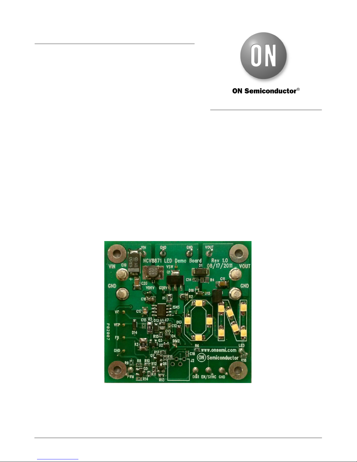
Figure 1. NCV887300 LED Evaluation Board
1 Publication Order Number:
EVBUM2181/D
Page 2

NCV887300LEDGEVB
Table 1. EVALUATION BOARD TERMINALS
Terminal Function
VIN Positive DC Input Voltage
GND Common DC Return
VOUT Regulated DC Output Voltage
EN/SYNC Enable and Synchronization Input
Table 2. ABSOLUTE MAXIMUM RATINGS (Voltages are with respect to GND)
Rating
DC Supply Voltage (VIN) −0.3 to 40 V
DC Supply Voltage (EN, SYNC) −0.3 to 6 V
Junction Temperature (NCV8902) −40 to 150 C
Ambient Temperature (Evaluation Board) −40 to 105 C
Value Unit
Table 3. ELECTRICAL CHARACTERISTICS (T
Characteristics
REGULATION
Load Current (Adjustable via R3)
SWITCHING
Switching Frequency
Soft-start Time − 1.66 ms
SYNC Frequency Range − 1.0−1.1 MHz
CURRENT LIMIT
Average Current Limit (Load)
Cycle-by-cycle Current Limit (FET) − 0.95 A
PROTECTIONS
Input Undervoltage Lockout (UVLO)
Thermal Shutdown TA Increasing 170 C
=25C, 6 V VIN V
A
Conditions Typical Value Unit
R3 = 3.32 W
− 1000 kHz
− 0.06 A
VIN Decreasing 3.05 V
, VEN= 2 V, unless otherwise specified)
out_LED
60 mA
http://onsemi.com
2
Page 3
Operational Guidelines
1. Connect a DC input voltage, within the 6 V to
40 V range, between VIN and GND.
2. Connect a DC enable voltage, within the 2.0 V to
5.0 V range, between EN/SYNC and GND.
3. Connect a function generator between PWM and
GND. It is recommended the waveform be set to:
125−200 Hz Square Typical Frequency Range
Low State Voltage of 0–0.8 V
High State of 1.8−5 V Range
Duty Cycle from 0.1% to 100%
4. Overvoltage may be tested by enabling the board
(EN/SYNC) with jumper J1 removed.
+
V
in
−
NCV887300LEDGEVB
5. Optionally:
for external clock synchronization, connect a
pulse source between EN/SYNC and GND. The
high state level should be within the 1.8 to 5 V
range
to 0.8 V range, with a minimum pulse width of
40 ns and a frequency within the 1 MHz and
1.1 MHz range.
Jumper J1 should be removed if an external load
is to be used instead of on-board LEDs. Input
voltage operating range is valid for loads
requiring V
*
, and the low state level within the −0.3 V
<40V.
out
Optional Load
(Must Remove J1)
PWM
Dimming
Figure 2. Evaluation Board Connections
*The dimming frequency interface circuit may be configured to accept either an 1.8 V or a 3.3 V/5 V control signal (refer to schematic). For a
1.8 V signal, use BOM and schematic as is. For a 3.3 V/5 V control signal, components R8, R9, R10, R11, Q6 are optional (R14 = 3.01K if
mentioned components are removed).
V
enable
+
−
http://onsemi.com
3
Page 4

NCV887300LEDGEVB
TYPICAL PERFORMANCE − START-UP
VOUT
EN
Figure 3. Typical Start-up with VIN = 6 V,
10 LEDs/60 mA
VOUT
EN
VOUT
EN
Figure 4. Typical Start-up with VIN = 12 V,
10 LEDs/60 mA
PWM
GDRV
VFB
VC
Figure 5. Typical Start-up with VIN = 18 V,
10 LEDs/60 mA
Figure 7. Converter Operation during 200 Hz 1000:1 Dimming,
V
IN
Figure 6. Converter Operation during Dimming,
= 12 V, 10 LEDs/60 mA
http://onsemi.com
4
V
= 12 V, 10 LEDs/60 mA
IN
PWM
GDRV
VFB
VC
Page 5

NCV887300LEDGEVB
SCHEMATIC
Figure 8. NCV887300 Boost LED Evaluation Board Schematic
(Applicable to PCB Rev 1.0 dated 08/11/2011)
Figure 9. NCV887300 Boost LED Evaluation Board Schematic
(Applicable to PCB Rev 1.0 dated 02/27/2013)
http://onsemi.com
5
Page 6

NCV887300LEDGEVB
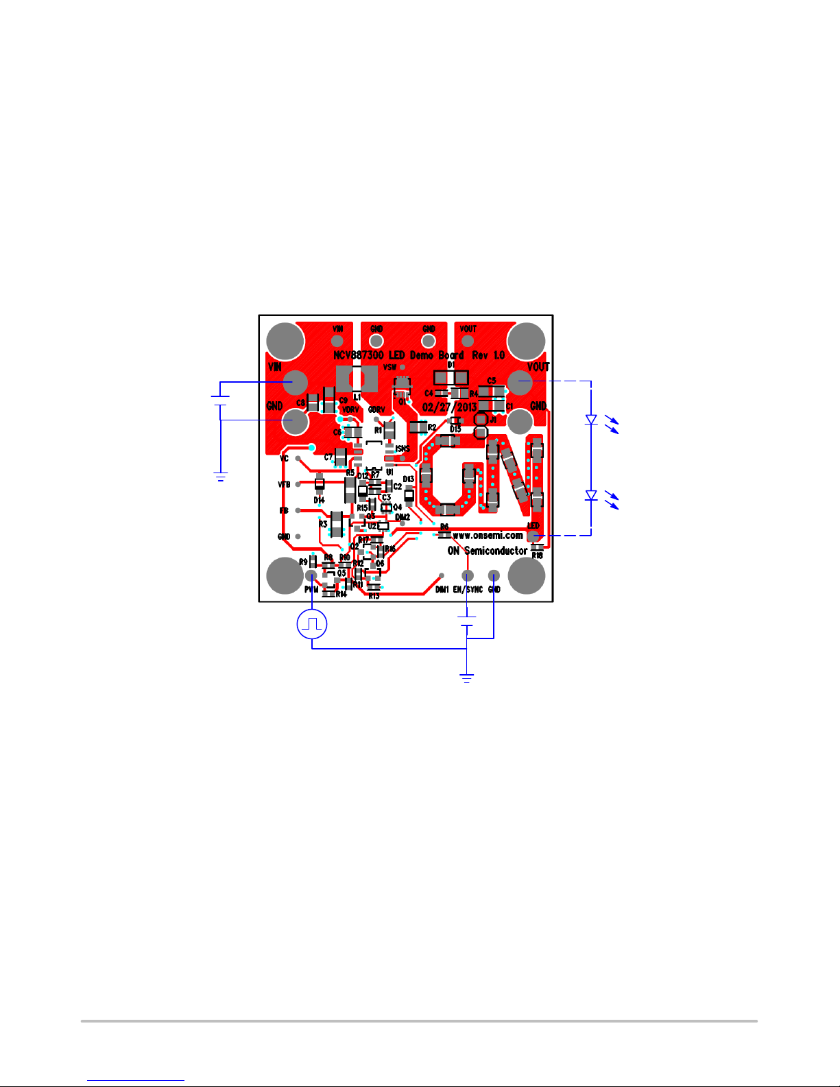
PCB LAYOUT
Figure 10. Top View
Figure 11. Bottom View
http://onsemi.com
6
Page 7

Table 4. BILL OF MATERIALS
Reference
Designator(s)
C1 1 OPEN Do Not
C2 1 CAP CER 1000 pF 50 V
C3 1 CAP CER 4.7 pF 50 V
C4 1 OPEN Do Not
C5 1
C6 1
C7 1
C8 1
C9 1 OPEN Do Not
D1 1 Diode Ultra Fast 2 A 100 V
D2 through D11 10 LED DURIS P5 29 LM
D12, D13, D14 3 Diode SGL JUNC 100 V
D15 1 Diode Zener 33 V 220 MW
J1
L1 1 SMT Power Inductor
Q1 1 MOSFET N-CH 60 V 20 A
Q2 1 PNP, Small Signal, −40 V,
Q3 1 MOSFET 50 V 200 mA
Q4 1 MOSFET 30 V 250 mA
Q5, Q6 2 NPN, Small Signal, 40 V,
R1 1
R2 1
R3 1
R4 1 OPEN Do Not
R5 1
R6, R16 2
R7 1
R8, R10, R11 3
R9, R12, R17 3
R13 1
R14 1 OPEN Do Not
Quantity Description Value Tolerance Manufacturer
X7R 0603
NP0 0603
CAP CER 2.2 mF 50 V
X7R 1206
CAP CER 1 mF 16 V 10%
X7R 0805
CAP CER 0.1 mF 50 V
10% X7R 0805
CAP CER 4.7 mF 50 V
10% X5R 0805
SMA
4000K
4.0NS MELF
SOD−323
1 CONN HEADER
1 CONN JUMPER
2POS.100 VERT GOLD
SHORTING GOLD
3.3 mH 1.33 A Isat
m8FL
SOT−23
3.5 W N-channel SOT−23
1.5 W Dual N-channel
SOT−23
RES 0.0 W 1/8 W 0805
SMD
RES 0.43 W 1/4 W 1%
0805 SMD
RES 3.32 W 1/4 W 1%
1206 SMD
RES 11.0 W 1/4 W 1%
1206 SMD
RES 10 kW 1/10 W 1%
0603 SMD
RES 18.2 kW 1/10 W 1%
0603 SMD
RES 3.01 kW 1/10 W 1%
0603 SMD
RES 1.00 kW 1/10 W 1%
0603 SMD
RES 499 W 1/10 W 1%
0603 SMD
NCV887300LEDGEVB
Manufacturer’s
Part Number
Populate
1000 pF,
50 V
4.7 pF, 50 V 5% Murata Electronics
Populate
2.2 mF, 50 V
1 mF, 16 V
0.1 mF, 50 V
4.7 mF, 50 V
Populate
100 V, 2 A N/A ON Semiconductor MURA110T3G
N/A N/A OSRAM Opto
N/A N/A ON Semiconductor MMSD4148T1G
33 V 5% ON Semiconductor MM3Z33VT1G
N/A N/A Molex Connector
N/A N/A Sullins Connector
3.3 mH
60 V, 20 A N/A ON Semiconductor NVTFS5826NL
−40 V, 0.2 A N/A ON Semiconductor MMBT3906LT1G
50 V, 0.2 A N/A ON Semiconductor BSS138LT1G
30 V, 0.25 A N/A ON Semiconductor NTJD4001N
40 V, 0.2 A N/A ON Semiconductor MMBT3904LT1G
0 W
0.43 W
3.32 W
Populate
11 W
10.0 kW
18.2 kW
3.01 kW
1.00 kW
499 W
Populate
10% Murata Electronics
10% Murata Electronics
10% Kemet C0805C105K4RACAUTO
10% Murata Electronics
10% TDK Corporation CGA4J3X5R1H475K125AB
20% Coilcraft Inc MSS5131−332MLB
JUMPER Vishay/Dale CRCW08050000Z0EA
1% Rohm Semiconductor MCR10EZHFLR430
1% Vishay/Dale CRCW12063R32FKEA
1% Vishay/Dale CRCW120611R0FKEA
1% Vishay/Dale CRCW060310K0FKEA
1% Vishay/Dale CRCW060318K2FKEA
1% Vishay/Dale CRCW06033K01FKEA
1% Vishay/Dale CRCW06031K00FKEA
1% Vishay/Dale CRCW0603499RFKEA
North America
North America
North America
North America
Semiconductor Inc
Corporation
Solutions
GCM188R71H102KA37D
GCM1885C1H4R7CZ13D
GRM31CR71H225KA88L
GRM21BR71H104KA01L
GW DASPA1.EC−GUHQ−5L7N−1D12
22−28−4023
SSC02SYAN
http://onsemi.com
7
Page 8

Table 4. BILL OF MATERIALS (continued)
Reference
Designator(s)
R15 1
R18 1
TP1, TP4, TP7,
TP14, TP16,
TP17, TP20, TP22
TP2, TP3, TP5,
TP6, TP8, TP9,
TP15, TP18,
TP19, TP21
TP10, TP11, TP12,
TP13
U1 1 Automotive Non-Sync
U2 1 IC BUFF CMOS LVL/SFTR
MNT1, 2, 3, 4
10 CICRUIT PIN PRNTD
RES 4.99 kW 1/10 W 1%
0603 SMD
RES 100 kW 1/10 W 1%
0603 SMD
8 PIN INBOARD .42 HOLE
4 TERM SOLDER TURRET
4 Hex Spacer 4−40 1/4 Zinc
4 Hex Nut 4−40 1/4 Zinc
1000/PKG
.020 D .425 L
.219 .109 L
Boost Controller
N-I SOT353
Plated Steel 3/8
Plated Steel
NCV887300LEDGEVB
ManufacturerToleranceValueDescriptionQuantity
4.99 kW
100 kW
N/A N/A Vector Electronics K24C/M
Do Not
Populate
N/A N/A Mill-Max
N/A N/A ON Semiconductor NCV887300D1R2G
N/A N/A ON Semiconductor M74VHC1GT50DFT1G
N/A N/A McMaster-Carr 93620A431
N/A N/A McMaster-Carr 90480A005
1% Vishay/Dale CRCW06034K99FKEA
1% Vishay/Dale CRCW0603100KFKEA
Mill-Max
Manufacturing Corp.
Manufacturing Corp.
3128−2−00−15−00−00−08−0
2501−2−00−44−00−00−07−0
Manufacturer’s
Part Number
ON Semiconductor and are registered trademarks of Semiconductor Components Industries, LLC (SCILLC). SCILLC owns the rights to a number of patents, trademarks,
copyrights, trade secrets, and other intellectual property. A listing of SCILLC’s product/patent coverage may be accessed at www.onsemi.com/site/pdf/Patent−Marking.pdf. SCILLC
reserves the right to make changes without further notice to any products herein. SCILLC makes no warranty, representation or guarantee regarding the suitability of its products for any
particular purpose, nor does SCILLC assume any liability arising out of the application or use of any product or circuit, and specifically disclaims any and all liability, including without
limitation special, consequential or incidental damages. “Typical” parameters which may be provided in SCILLC data sheets and/or specifications can and do vary in different applications
and actual performance may vary over time. All operating parameters, including “Typicals” must be validated for each customer application by customer’s technical experts. SCILLC
does not convey any license under its patent rights nor the rights of others. SCILLC products are not designed, intended, or authorized for use as components in systems intended for
surgical implant into the body, or other applications intended to support or sustain life, or for any other application in which the failure of the SCILLC product could create a situation where
personal injury or death may occur. Should Buyer purchase or use SCILLC products for any such unintended or unauthorized application, Buyer shall indemnify and hold SCILLC and
its officers, employees, subsidiaries, affiliates, and distributors harmless against all claims, costs, damages, and expenses, and reasonable attorney fees arising out of, directly or indirectly,
any claim of personal injury or death associated with such unintended or unauthorized use, even if such claim alleges that SCILLC was negligent regarding the design or manufacture
of the part. SCILLC is an Equal Opportunity/Affirmative Action Employer. This literature is subject to all applicable copyright laws and is not for resale in any manner.
PUBLICATION ORDERING INFORMATION
LITERATURE FULFILLMENT:
Literature Distribution Center for ON Semiconductor
P.O. Box 5163, Denver, Colorado 80217 USA
Phone: 303−675−2175 or 800−344−3860 Toll Free USA/Canada
Fax: 303−675−2176 or 800−344−3867 Toll Free USA/Canada
Email: orderlit@onsemi.com
N. American Technical Support: 800−282−9855 Toll Free
USA/Canada
Europe, Middle East and Africa Technical Support:
Phone: 421 33 790 2910
Japan Customer Focus Center
Phone: 81−3−5817−1050
http://onsemi.com
8
ON Semiconductor Website: www.onsemi.com
Order Literature: http://www.onsemi.com/orderlit
For additional information, please contact your local
Sales Representative
EVBUM2181/D
Page 9

Mouser Electronics
Authorized Distributor
Click to View Pricing, Inventory, Delivery & Lifecycle Information:
ON Semiconductor:
NCV8873LEDBSTGEVB
 Loading...