

NCV8505 Series
Micropower 400 mA
LDO Linear Regulators
with ENABLE, DELAY,
and RESET
The NCV8505 is a family of precision micropower voltage
regulators. Their output current capability is 400 mA. The family has
output voltage options for Adjustable, 2.5 V, 3.3 V and 5.0 V.
The output voltage is accurate within ± 2.0% with a maximum
dropout voltage of 0.6 V at 400 mA. Low quiescent current is a feature
drawing less than 1.0 µA w ith E NABLE = 0 V. With ENABLE = 5.0 V,
the part only draws 200 µA with 100 µA load. This part is ideal for any
and all battery operated microprocessor equipment.
Microprocessor control logic includes an active RESET
DELAY).
The active RESET circuit operates correctly at an output voltage as
low as 1.0 V. The RESET
function is activated during the power up
sequence or during normal operation if the output voltage drops below
the regulation limits.
The regulator is protected against reverse battery, short circuit, and
thermal overload conditions. The device can withstand load dump
transients making it suitable for use in automotive environments. The
device has also been optimized for EMC conditions.
Features
• Output Voltage Options: Adjustable, 2.5 V, 3.3 V, 5.0 V
• ± 2.0% Output
• Low < 1.0 µA Sleep Current
• Low 200 µA Quiescent Current
• Fixed or Adjustable Output Voltage
• Active RESET
• ENABLE
• 400 mA Output Current Capability
• Fault Protection
♦ +60 V Peak Transient Voltage
♦ −15 V Reverse Voltage
♦ Short Circuit
♦ Thermal Overload
• NCV Prefix for Automotive and Other Applications Requiring Site
and Change Control
(with
http://onsemi.com
MARKING
DIAGRAM
NCV8505x
AWLYYWW
2
D
PAK−7
DPS SUFFIX
CASE 936AB
x = Voltage Ratings as Indicated Below:
A = Adjustable
2 = 2.5 V
3 = 3.3 V
5 = 5.0 V
A = Assembly Location
WL = Wafer Lot
YY = Year
WW = Work Week
ORDERING INFORMATION
See detailed ordering and shipping information in the package
dimensions section on page 11 of this data sheet.
1
Semiconductor Components Industries, LLC, 2004
January, 2004 − Rev. 3
1 Publication Order Number:
NCV8505/D
NCV8505 Series
PIN CONNECTIONS
FIXED OUTPUTADJUSTABLE OUTPUT
Tab = GND
Lead 1. DELAY
2. ENABLE
3. RESET
4. GND
5. V
ADJ
6. V
OUT
7. V
1
IN
1
Tab = GND
Lead 1. DELAY
2. ENABLE
3. RESET
4. GND
5. SENSE
6. V
OUT
7. V
IN
SENSE
I
V
BAT
Q
10 µF
C
DELAY
(Fixed Output Only)
V
IN
NCV8505
DELAY
V
OUT
V
ADJ
(Adjustable
Output Only)
R
RST
5.1 k
33 µF
V
DD
Microprocessor
ENABLE
GND
RESET
Figure 1. Application Diagram
I/O
http://onsemi.com
2
NCV8505 Series
MAXIMUM RATINGS*
Rating Value Unit
V
(DC) −15 to 45 V
IN
Peak Transient Voltage (46 V Load Dump @ VIN = 14 V) 60 V
Operating Voltage 45 V
V
(DC) 16 V
OUT
Voltage Range (RESET, DELAY) −0.3 to 10 V
Input Voltage Range: V
ADJ
Input Voltage Range (ENABLE) −0.3 to 10** V
ESD Susceptibility (Human Body Model)
(Machine Model)
Junction Temperature, T
Storage Temperature, T
Package Thermal Resistance, 7 Lead D2PAK Junction−to−Case, R
J
S
θ
Junction−to−Ambient, R
JC
θ
JA
Lead Temperature Soldering: Reflow: (SMD styles only) (Note 1) 240 peak (Note 2) °C
1. 60 second maximum above 183°C.
2. −5°C/+0°C allowable conditions.
*The maximum package power dissipation must be observed.
**Reference Figure 14 for switched−battery ENABLE application.
= R
+ R
***Depending on thermal properties of substrate, R
†During the voltage range which exceeds the maximum tested voltage of V
JA
JC
Thermal dissipation must be observed closely.
.
CA
, operation is assured, but not specified. Wider limits may apply.
IN
−0.3 to 16 V
4.0
200
−40 to +150 °C
−55 to 150 °C
2.0
10−50***
kV
V
°C/W
°C/W
ELECTRICAL CHARACTERISTICS (I
= 1.0 mA, ENABLE = 5.0 V, −40°C ≤ T
OUT
≤ 150°C; VIN = dependent on voltage option
J
(Note 3); unless otherwise specified.)
Characteristic
Test Conditions Min Typ Max Unit
Output Stage
Output Voltage for 2.5 V Option (V
Output Voltage for 3.3 V Option (VO) 7.3 V < VIN < 16 V, 1.0 mA ≤ I
Output Voltage for 5.0 V Option (VO) 9.0 V < VIN < 16 V, 1.0 mA ≤ I
Output Voltage for Adjustable Option
(V
)
O
Dropout Voltage (VIN − V
OUT
(5.0 V and Adj. > 5.0 V Options Only)
Load Regulation VIN = 14 V, 5.0 mA ≤ I
Line Regulation (2.5 V, 3.3 V, and
) 6.5 V < VIN < 16 V, 1.0 mA ≤ I
O
)
4.5 V < V
4.5 V < V
6.0 V < V
V
= V
OUT
6.5 V < V
4.5 V < V
I
= 400 mA
OUT
I
= 1.0 mA
OUT
< 26 V, 1.0 mA ≤ I
IN
< 26 V, 1.0 mA ≤ I
IN
< 26 V, 1.0 mA ≤ I
IN
(Unity Gain)
ADJ
< 16 V, 1.0 mA < I
IN
< 26 V, 1.0 mA < I
IN
4.5 V < VIN < 26 V, I
≤ 400 mA
OUT
≤ 400 mA
OUT
≤ 400 mA
OUT
≤ 400 mA
OUT
≤ 400 mA
OUT
≤ 400 mA
OUT
< 400 mA
OUT
< 400 mA
OUT
≤ 400 mA −30 5.0 30 mV
OUT
= 1.0 mA − 5.0 25 mV
OUT
2.450
2.425
3.234
3.201
4.90
4.85
1.274
1.261
−
−
2.5
2.5
3.3
3.3
5.0
5.0
1.300
1.300
400
30
2.550
2.575
3.366
3.399
5.10
5.15
1.326
1.339
600
150
Adjustable Options)
Line Regulation (5.0 V Option) 6.0 V < VIN < 26 V, I
Quiescent Current, (IQ) Active Mode I
= 100 µA, VIN = 12 V
OUT
I
= 75 mA, VIN = 14 V
OUT
≤ 400 mA, VIN = 14 V
I
OUT
= 1.0 mA − 5.0 25 mV
OUT
−
−
−
200
2.5
25
350
5.0
45
Quiescent Current, (IQ) Sleep Mode ENABLE = 0 V, VIN = 12 V, −40°C ≤ TJ ≤ 125°C − − 1.0 µA
Current Limit − 425 800 − mA
Short Circuit Output Current V
= 0 V 100 500 − mA
OUT
Thermal Shutdown (Guaranteed by Design) 150 180 − °C
3. Voltage range specified in the Output Stage of the Electrical Characteristics in boldface type.
V
V
V
V
V
V
V
V
mV
mV
µA
mA
mA
http://onsemi.com
3
NCV8505 Series
ELECTRICAL CHARACTERISTICS (continued) (I
= 1.0 mA, ENABLE = 5.0 V, −40°C ≤ T
OUT
≤ 150°C; VIN = dependent on
J
voltage option (Note 4); unless otherwise specified.)
Characteristic
Test Conditions Min Typ Max Unit
Reset Function (RESET)
RESET Threshold for 2.5 V Option
HIGH (V
LOW (V
RL
RH
)
)
Hysteresis
RESET Threshold for 3.3 V Option
HIGH (V
LOW (V
RL
RH
)
)
Hysteresis
RESET Threshold for 5.0 V Option
RL
RH
)
)
HIGH (V
LOW (V
Hysteresis
RESET Threshold for Adjustable Option
HIGH (V
LOW (V
RL
RH
)
)
Hysteresis
Output Voltage
Low (V
RLO
)
DELAY Switching Threshold (VDT)
VIN = 4.5 V (Note 5) (Note 6)
V
V
OUT
OUT
Increasing
Decreasing
2.35
2.30
25
−
1.0 × V
O
−
−
−
−
VIN = 4.5 V (Note 5) (Note 6)
V
V
OUT
OUT
Increasing
Decreasing
3.10
3.00
35
−
1.0 × V
O
−
−
−
−
VIN = 6.0 V (Note 6)
V
V
OUT
OUT
Increasing
Decreasing
4.70
4.60
50
−
1.0 × V
−
−
O
−
−
VIN = 4.5 V (Note 5) (Note 6)
V
Increasing
OUT
Decreasing
V
OUT
VIN = Minimum (Note 6) (Note 7)
1.0 V ≤ V
OUT
≤ VRL, R
RESET
= 5.1 k
1.22
1.19
10
−
1.0 × V
O
−
−
−
−
− 0.1 0.4 V
VIN = Minimum (Note 6) (Note 7) 1.4 1.8 2.2 V
(2.5 V, 3.3 V, and 5.0 V Options)
DELAY Switching Threshold (VDT)
VIN = Minimum (Note 6) (Note 7) 1.0 1.3 1.6 V
(Adjustable Option)
DELAY Low Voltage VIN = Minimum (Note 6) (Note 7)
V
< RESET Threshold Low(min)
OUT
DELAY Charge Current VIN = Minimum (Note 6) (Note 7)
DELAY = 1.0 V, V
OUT
> V
RH
DELAY Discharge Current VIN = Minimum (Note 6) (Note 7)
DELAY = 1.0 V, V
OUT
< V
RL
− − 0.2 V
2.5 4.0 5.5 µA
5.0 − − mA
Voltage Adjust (Adjustable Output only)
Input Current V
= 1.25 V, VIN = Minimum (Note 6) (Note 7) −0.5 − 0.5 µA
ADJ
ENABLE
Input Threshold Low, VIN = 14 V (Note 6)
High, V
= 14 V (Note 6)
IN
2.0
−
−
−
1.0
−
Input Current ENABLE = 5.0 V, VIN = 14 V (Note 6) − 30 75 µA
4. Voltage range specified in the Output Stage of the Electrical Characteristics in boldface type.
5. For V
6. Part is guaranteed by design to meet specification over the entire V
7. Minimum V
≤ 4.5 V, a RESET = Low may occur with the output in regulation.
IN
= 4.5 V for 2.5 V, 3.3 V, and Adjustable options. Minimum VIN = 6.0 V for 5.0 V option.
IN
voltage range, but is production tested only at the specified VIN voltage.
IN
V
V
mV
V
V
mV
V
V
mV
V
V
mV
V
V
http://onsemi.com
4
NCV8505 Series
PACKAGE PIN DESCRIPTION, ADJUSTABLE OUTPUT
Pin Number Pin Symbol Function
1 DELAY Timing capacitor for RESET function.
2 ENABLE ENABLE control for the IC. A high powers the device up.
3 RESET Active reset (accurate to V
4 GND Ground. All GND leads must be connected to Ground
5 V
6 V
7 V
ADJ
OUT
IN
Voltage Adjust. A resistor divider from V
±2.0%, 400 mA output.
Input Voltage.
PACKAGE PIN DESCRIPTION, FIXED OUTPUT
Pin Number Pin Symbol Function
1 DELAY Timing capacitor for RESET function.
2 ENABLE ENABLE control for the IC. A high powers the device up.
3 RESET Active reset (accurate to V
4 GND Ground. All GND leads must be connected to Ground
5 SENSE
6 V
7 V
OUT
IN
Kelvin connection which allows remote sensing of output voltage for improved regulation. If
remote sensing is not desired, connect to V
±2.0%, 400 mA output.
Input Voltage.
OUT
OUT
≥ 1.0 V)
≥ 1.0 V)
to this lead sets the output voltage.
OUT
OUT
.
.
.
http://onsemi.com
5
NCV8505 Series
V
V
IN
OUT
ENABLE
RESET
DELAY
+
−
Current Source
(Circuit Bias)
1.5 V
1.8 V (Fixed Versions)
1.3 V (Adjustable Version)
+
−
4.0 µA
I
BIAS
I
+
−
Thermal
Protection
Bandgap
Reference
I
BIAS
Figure 2. Block Diagram
BIAS
+
−
Error Amplifier
V
BG
VBG −18 mV
V
BG
Current Limit
Sense
Fixed Versions only
15 k
Adjustable
Version only
SENSE
V
ADJ
GND
http://onsemi.com
6
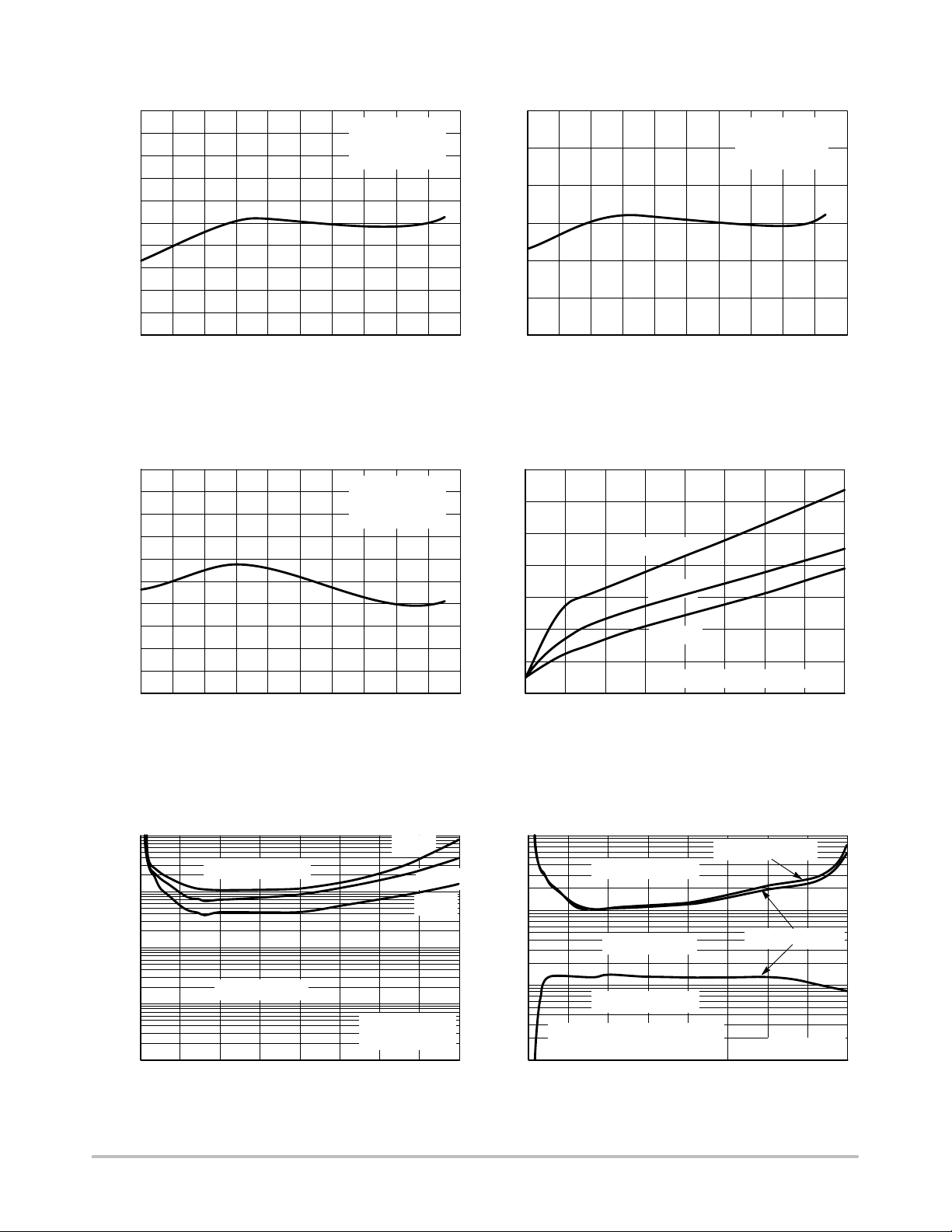
5.10
5.08
5.06
5.04
5.02
5.00
4.98
4.96
, OUTPUT VOLTAGE (V)
4.94
out
V
4.92
4.90
−40
TYPICAL PERFORMANCE CHARACTERISTICS
V
V
I
OUT
−20 1400 20 40 60 80 120100
TEMPERATURE (°C)
= 5.0 V
OUT
= 14 V
IN
= 5.0 mA
NCV8505 Series
3.35
3.33
3.31
3.29
3.27
, OUTPUT VOLTAGE (V)
out
3.25
V
3.23
160
−40
V
V
I
OUT
−20 1400 20 40 60 80 120100
TEMPERATURE (°C)
= 3.3 V
OUT
= 14 V
IN
= 5.0 mA
160
Figure 3. 5 V Output Voltage vs Temperature
2.55
2.54
2.53
2.52
2.51
2.50
2.49
2.48
, OUTPUT VOLTAGE (V)
2.47
out
V
2.46
2.45
−40
−20 1400 20 40 60 80 120100
TEMPERATURE (°C)
V
V
I
OUT
OUT
IN
= 2.5 V
= 14 V
= 5.0 mA
160
Figure 4. 3.3 V Output Voltage vs Temperature
700
600
500
400
300
200
DROPOUT VOLTAGE (mV)
100
0
0
50 100 150 200 250
I
125 °C
25 °C
−40 °C
5 V and Adj. > 5 V options only
, OUTPUT CURRENT (mA)
out
300 350 400
Figure 5. 2.5 V Output Voltage vs Temperature Figure 6. Dropout Voltage vs Output Current
100
10
Unstable Region
5.0 V
3.3 V
2.5 V
100
10
Unstable Region
C
VOUT
= 33 F*
C
= 0.1 F
VOUT
5 V version
ESR ()
1.0
0.1
0.01
Stable Region
VIN = 14 V
C
VOUT
0
50 100 150 200 250 350 400
, OUTPUT CURRENT (mA)
I
out
300
= 10 F
Stable Region
ESR ()
1.0
Unstable Region
*There is no unstable lower
0.1
region for the 33 F capacitor
0 300
50 100 150 200 250 350 400
, OUTPUT CURRENT (mA)
I
out
Figure 7. Output Stability with Output Voltage Change Figure 8. Output Stability with Output Capacitor Change
http://onsemi.com
7

NCV8505 Series
TYPICAL PERFORMANCE CHARACTERISTICS
2.0
1.8
1.6
1.4
+125°C
+25°C
−40°C
60
50
+25°C
40
1.2
1.0
30
0.8
0.6
0.4
, QUIESCENT CURRENT (mA)
Q
I
0.2
0.0
0
5101520 3025
, OUTPUT CURRENT (mA)
I
OUT
35 40 5045
20
10
, QUIESCENT CURRENT (mA)
Q
I
0
0
50
100
150 200 300250
, OUTPUT CURRENT (mA)
I
OUT
350 400 500450
Figure 9. Quiescent Current vs Output Current Figure 10. Quiescent Current vs Output Current
12
I
= 200 mA
out
10
8
6
I
= 100 mA
4
2
, QUIESCENT CURRENT (mA)
Q
I
0
6
8
out
I
out
I
out
10
12 14 1816
V
= 50 mA
= 10 mA
, INPUT VOLTAGE (V)
IN
T = 25°C
20 22 2624
, QUIESCENT CURRENT (A)
I
Q
210
205
200
195
190
185
180
175
I
= 100 A
out
6
10
8
12 14 1816
, INPUT VOLTAGE (V)
V
IN
20 22 2624
+125°C
−40°C
T = 25°C
Figure 11. Quiescent Current vs Input Voltage
http://onsemi.com
Figure 12. Quiescent Current vs Input Voltage
8

NCV8505 Series
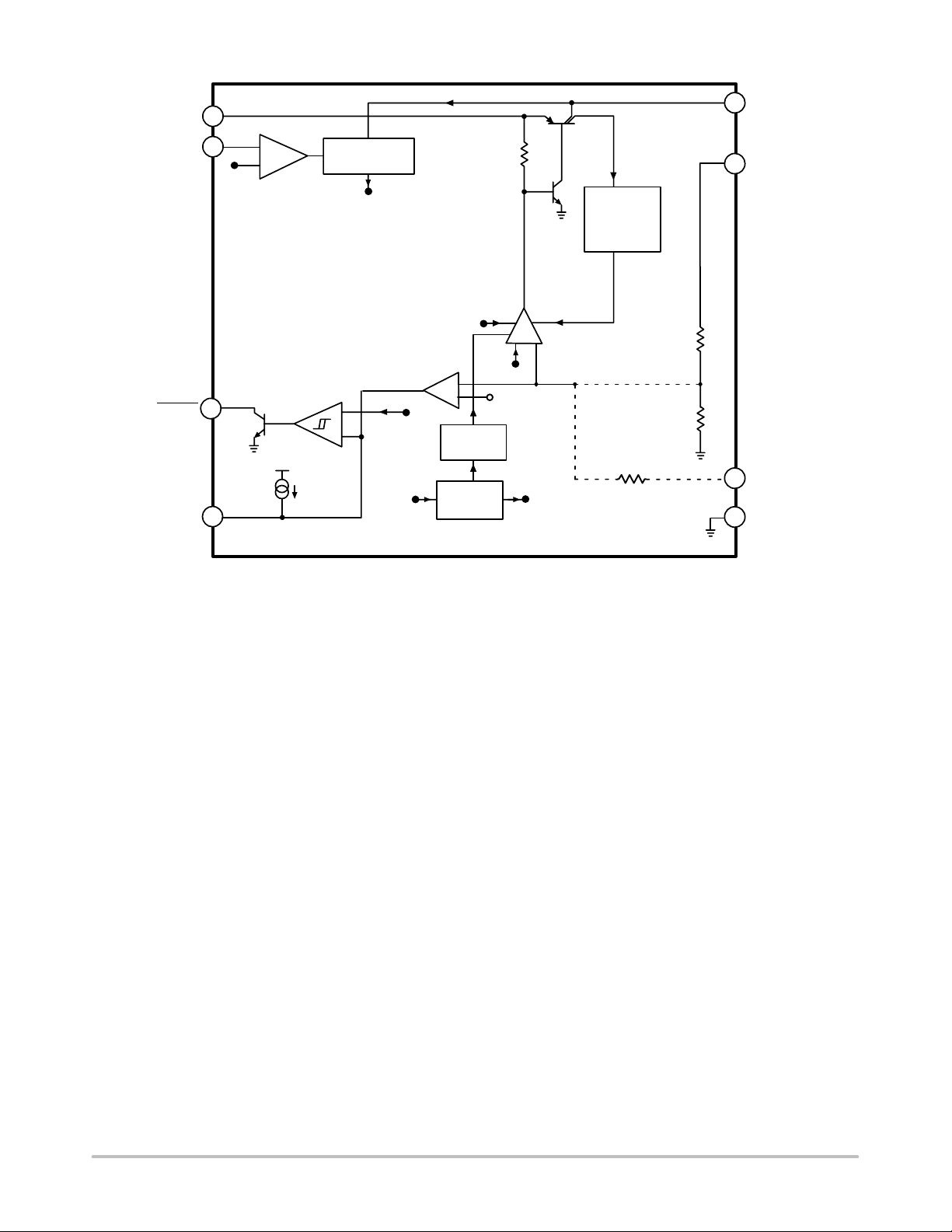
CIRCUIT DESCRIPTION
REGULATOR CONTROL FUNCTIONS
The NCV8505 contains the microprocessor compatible
control function RESET (Figure 13).
V
IN
V
OUT
DELAY
RESET
T
d
T
d
RESET
Threshold
DELAY
Threshold
(V
DT
Figure 13. Reset and Delay Circuit Wave Forms
RESET Function
A RESET signal (low voltage) is generated as the IC
powers up until V
voltage, or when V
is within 1.5% of the regulated output
OUT
drops out of regulation,and is lower
OUT
than 4.0% below the regulated output voltage. Hysteresis is
included in the function to minimize oscillations.
The RESET output is an open collector NPN transistor,
controlled by a low voltage detection circuit. The circuit is
functionally independent of the rest of the IC thereby
guaranteeing that the RESET
signal is valid for V
OUT
as low
as 1.0 V.
DELAY Function
The reset delay circuit provides a programmable (by
external capacitor) delay on the RESET output lead.
The DELAY lead p rovides s ource c urrent ( typically 4 .0 µA)
to the external DELAY capacitor during the following
proceedings:
1. During Power Up (once the regulation threshold
has been verified).
2. After a reset event has occurred and the device is
back in regulation. The DELAY capacitor is
discharged when the regulation (RESET
)
has been violated. This is a latched incident. The
capacitor will fully discharge and wait for the
device to regulate before going through the delay
time event again.
Voltage Adjust
Figure 15 shows the device setup for a user configurable
output voltage. The feedback to the V
pin is taken from
ADJ
a voltage divider referenced to the output voltage. The loop
is balanced around the Unity Gain threshold (1.30 V
typical).
V
NCV8505
V
OUT
ADJ
15 k
1.28 V
≈5.0 V
threshold)
C
OUT
ENABLE Function
The part stays in a low IQ sleep mode when the ENABLE
pin is held low. The part has an internal pull down if the pin
is left floating.
The integrity of the ENABLE pin allows it to be tied to the
battery line through an external resistor. It will withstand
load dump potentials in this configuration.
V
BAT
Up to 45 V
10 k
V
IN
NCV8505
ENABLE
Figure 14. ENABLE Function
GND
V
OUT
5.1 k
Figure 15. Adjustable Output Voltage
http://onsemi.com
9

NCV8505 Series
APPLICATION NOTES
SETTING THE DELAY TIME
The delay time is controlled by the Reset Delay Low
Voltage, Delay Switching Threshold, and the Delay Charge
Current. The delay follows the equation:
t
DELAY
[
C
DELAY(Vdt
Delay Charge Current
Reset Delay Low Voltage)
]
Example:
Using C
DELAY
= 33 nF.
Assume reset Delay Low Voltage = 0.
Use the typical value for V
= 1.8 V (2.5 V, 3.3 V, and
dt
5.0 V options).
Use the typical value for Delay Charge Current = 4.2 µA.
t
DELAY
[
33 nF(1.8 0)
4.2 A
]
14 ms
STABILITY CONSIDERATIONS
The output or compensation capacitor helps determine
three main characteristics of a linear regulator: start−up
delay , load transient response and loop stability.
The capacitor value and type should be based on cost,
availability, size and temperature constraints. A tantalum or
aluminum electrolytic capacitor is best, since a film or
ceramic capacitor with almost zero ESR can cause
instability. The aluminum electrolytic capacitor is the least
expensive solution, but, if the circuit operates at low
temperatures (−25°C to −40°C), both the value and ESR of
the capacitor will vary considerably. The capacitor
manufacturers data sheet usually provides this information.
The value for the output capacitor C
shown i n F igure 16
OUT
should work for most applications, however it is not
necessarily the optimized solution.
P
D(max)
[V
V
IN(max)
IN(max)IQ
V
OUT(min)]IOUT(max)
(1)
where:
V
V
I
OUT(max)
is the maximum input voltage,
IN(max)
OUT(min)
is the minimum output voltage,
is the maximum output current for the
application, and
IQ is the quiescent current the regulator consumes at
I
OUT(max)
Once the value of P
permissible value of R
The value of R
.
is known, the maximum
D(max)
can be calculated:
JA
R
JA
150°C
JA
can then be compared with those in the
T
A
P
D
(2)
package section of the data sheet. Those packages with
R
’s less than the calculated value in equation 2 will keep
JA
the die temperature below 150°C.
In some cases, none of the packages will be sufficient to
dissipate the heat generated by the IC, and an external
heatsink will be required.
I
IN
V
IN
Figure 17. Single Output Regulator with Key
Performance Parameters Labeled
SMART
REGULATOR
Control
}
Features
I
Q
I
OUT
V
OUT
V
IN
CIN*
0.1 µF
*CIN required if regulator is located far from the power supply
filter.
required for stability. Capacitor must operate at minimum
**C
OUT
temperature expected.
Figure 16. Test and Application Circuit Showing
NCV8505
Output Compensation
V
OUT
RESET
C
R
RST
OUT
33 µF
CALCULATING POWER DISSIPATION IN A
SINGLE OUTPUT LINEAR REGULATOR
The maximum power dissipation for a single output
regulator (Figure 17) is:
http://onsemi.com
HEAT SINKS
A heat sink effectively increases the surface area of the
**
package to improve the flow of heat away from the IC and
into the surrounding air.
Each material in the heat flow path between the IC and the
outside environment will have a thermal resistance. Like
series electrical resistances, these resistances are summed to
determine the value of R
R
R
JA
JC
JA
R
:
CS
R
SA
(3)
where:
R
= the junction−to−case thermal resistance,
JC
R
= the case−to−heatsink thermal resistance, and
CS
R
= the heatsink−to−ambient thermal resistance.
SA
R
appears in the package section of the data sheet. Like
JC
R
, it too is a function of package type. R
JA
CS
and R
are
SA
functions of the package type, heatsink and the interface
between them. These values appear in heat sink data sheets
of heat sink manufacturers.
10
NCV8505 Series
ORDERING INFORMATION
Device Output Voltage Package Shipping†
NCV8505D2TADJ
NCV8505D2TADJR4
NCV8505D2T25
NCV8505D2T25R4
NCV8505D2T33
NCV8505D2T33R4
NCV8505D2T50
NCV8505D2T50R4
†For information on tape and reel specifications, including part orientation and tape sizes, please refer to our Tape and Reel Packaging
Specifications Brochure, BRD8011/D.
Adjustable
2.5 V
D2PAK−7
3.3 V
5.0 V
50 Units/Rail
750 Tape & Reel
50 Units/Rail
750 Tape & Reel
50 Units/Rail
750 Tape & Reel
50 Units/Rail
750 Tape & Reel
http://onsemi.com
11

NCV8505 Series
PACKAGE DIMENSIONS
D2PAK−7
DPS SUFFIX
CASE 936AB−01
ISSUE O
For D2PAK Outline and
Dimensions − Contact Factory
SMART REGULATOR is a registered trademark of Semiconductor Components Industries, LLC (SCILLIC).
ON Semiconductor and are registered trademarks of Semiconductor Components Industries, LLC (SCILLC). SCILLC reserves the right to make changes without further notice
to any products herein. SCILLC makes no warranty, representation or guarantee regarding the suitability of its products for any particular purpose, nor does SCILLC assume any liability
arising out of the application or use of any product or circuit, and specifically disclaims any and all liability, including without limitation special, consequential or incidental damages.
“Typical” parameters which may be provided in SCILLC data sheets and/or specifications can and do vary in different applications and actual performance may vary over time. All
operating parameters, including “Typicals” must be validated for each customer application by customer’s technical experts. SCILLC does not convey any license under its patent rights
nor the rights of others. SCILLC products are not designed, intended, or authorized for use as components in systems intended for surgical implant into the body, or other applications
intended to support or sustain life, or for any other application in which the failure of the SCILLC product could create a situation where personal injury or death may occur. Should
Buyer purchase or use SCILLC products for any such unintended or unauthorized application, Buyer shall indemnify and hold SCILLC and its officers, employees, subsidiaries, affiliates,
and distributors harmless against all claims, costs, damages, and expenses, and reasonable attorney fees arising out of, directly or indirectly, any claim of personal injury or death
associated with such unintended or unauthorized use, even if such claim alleges that SCILLC was negligent regarding the design or manufacture of the part. SCILLC is an Equal
Opportunity/Affirmative Action Employer. This literature is subject to all applicable copyright laws and is not for resale in any manner.
PUBLICATION ORDERING INFORMATION
LITERATURE FULFILLMENT:
Literature Distribution Center for ON Semiconductor
P.O. Box 5163, Denver, Colorado 80217 USA
Phone: 303−675−2175 or 800−344−3860 Toll Free USA/Canada
Fax: 303−675−2176 or 800−344−3867 Toll Free USA/Canada
Email: orderlit@onsemi.com
N. American Technical Support: 800−282−9855 Toll Free
USA/Canada
Japan: ON Semiconductor, Japan Customer Focus Center
2−9−1 Kamimeguro, Meguro−ku, Tokyo, Japan 153−0051
Phone: 81−3−5773−3850
http://onsemi.com
ON Semiconductor Website: http://onsemi.com
Order Literature: http://www.onsemi.com/litorder
For additional information, please contact your
local Sales Representative.
NCV8505/D
12

WWW.ALLDATASHEET.COM
Copyright © Each Manufacturing Company.
All Datasheets cannot be modified without permission.
This datasheet has been download from :
www.AllDataSheet.com
100% Free DataSheet Search Site.
Free Download.
No Register.
Fast Search System.
www.AllDataSheet.com
 Loading...