

Page 1
Self-Protected Low Side
Driver with In-Rush Current
Management
NCV8415
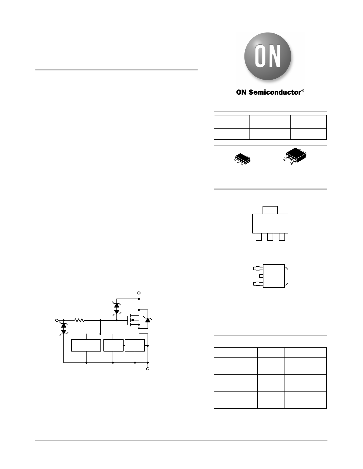
The NCV8415 is a three terminal protected Low−Side Smart
Discrete FET. The protection features include Delta Thermal
Shutdown, overcurrent, overtemperature, ESD and integrated
Drain−to−Gate clamping for overvoltage protection. The device also
offers fault indication via the gate pin. This device is suitable for harsh
automotive environments.
Features
• Short−Circuit Protection with In−Rush Current Management
• Delta Thermal Shutdown
• Thermal Shutdown with Automatic Restart
• Overvoltage Protection
• Integrated Clamp for Overvoltage Protection and Inductive
Switching
• ESD Protection
• dV/dt Robustness
• Analog Drive Capability (Logic Level Input)
• NCV Prefix for Automotive and Other Applications Requiring
Unique Site and Control Change Requirements; AEC−Q101 Grade 1
Qualified and PPAP Capable
• These Devices are Pb−Free and are RoHS Compliant
Typical Applications
• Switch a Variety of Resistive, Inductive and Capacitive Loads
• Can Replace Electromechanical Relays and Discrete Circuits
• Automotive / Industrial
Drain
Gate
Input
ESD Protection
Overvoltage
Protection
www.onsemi.com
V
DSS
(Clamped)
42 V
SOT−223
CASE 318E
STYLE 3
R
TYP
DS(ON)
80 mW @ 10 V
DPAK
CASE 369C
STYLE 2
MARKING DIAGRAMS
4
AYW
8415G
G
1
23
SOT−223
1
AYWW
2
NCV
8415G
3
DPAK
A = Assembly Location
Y = Year
W, WW = Work Week
G or G = Pb−Free Package
(Note: Microdot may be in either location)
4
MAX
I
D
(Limited)
11 A
Pin Marking
Information
1 = Gate
2 = Drain
3 = Source
4 = Drain
Temperature
Limit
Current
Limit
Figure 1. Block Diagram
© Semiconductor Components Industries, LLC, 2018
January, 2021 − Rev. 0
Current
Sense
Source
ORDERING INFORMATION
Device Package Shipping
NCV8415DTRKG DPAK
NCV8415STT1G SOT−223
NCV8415STT3G SOT−223
†For information on tape and reel specifications,
including part orientation and tape sizes, please
refer to our Tape and Reel Packaging Specification
Brochure, BRD8011/D.
1 Publication Order Number:
(Pb−Free)
(Pb−Free)
(Pb−Free)
Tape & Reel
Tape & Reel
Tape & Reel
†
2500 /
1000 /
4000 /
NCV8415/D
Page 2
NCV8415
MAXIMUM RATINGS
Rating Symbol Value Unit
Drain−to−Source Voltage Internally Clamped V
Drain−to−Gate Voltage Internally Clamped V
Gate−to−Source Voltage V
Drain Current − Continuous I
Total Power Dissipation (SOT−223)
@ T
= 25°C (Note 1)
A
@ TA = 25°C (Note 2)
DSS
DG
GS
D
P
D
Total Power Dissipation (DPAK)
@ TA = 25°C (Note 1)
@ T
= 25°C (Note 2)
A
Thermal Resistance (SOT−223)
Junction−to−Ambient (Note 1)
Junction−to−Ambient (Note 2)
Junction−to−Case (Soldering Point)
R
q
JA
R
q
JA
R
q
JS
Thermal Resistance (DPAK)
Junction−to−Ambient (Note 1)
Junction−to−Ambient (Note 2)
Junction−to−Case (Soldering Point)
Single Pulse Inductive Load Switching Energy (L = 10 mH, I
T
= 25°C)
Jstart
= 4.2 A, VGS = 5 V, RG = 25 W,
Lpeak
Load Dump Voltage (VGS = 0 and 10 V, RL = 10 W) (Note 3)
Operating Junction Temperature T
Storage Temperature T
R
q
JA
R
q
JA
R
q
JS
E
AS
US* 52 V
J
storage
Stresses exceeding those listed in the Maximum Ratings table may damage the device. If any of these limits are exceeded, device functionality
should not be assumed, damage may occur and reliability may be affected.
1. Mounted onto a 80 × 80 × 1.6 mm single layer FR4 board (100 sq mm, 1 oz. Cu, steady state).
2. Mounted onto a 80 × 80 × 1.6 mm single layer FR4 board (645 sq mm, 1 oz. Cu, steady state).
3. Load Dump Test B (with centralized load dump suppression) according to ISO16750−2 standard. Guaranteed by design. Not tested in
production. Passed Class C according to ISO16750−1.
42 V
42 V
±14 V
Internally Limited
W
1.29
2.20
1.54
2.99
°C/W
96.4
56.8
10.6
80.8
41.8
3.2
88 mJ
−40 to 150 °C
−55 to 150 °C
ESD ELECTRICAL CHARACTERISTICS (Note 4, 5)
Parameter
Electro−Static Discharge Capability
Human Body Model (HBM)
Charged Device Model (CDM) 1000 − −
4. Not tested in production.
5. This device series incorporates ESD protection and is tested by the following methods:
ESD Human Body Model tested per AEC−Q100−002 (JS−001−2017).
Field Induced Charge Device Model ESD characterization is not performed on plastic molded packages with body sizes smaller than
2 × 2 mm due to the inability of a small package body to acquire and retain enough charge to meet the minimum CDM discharge current
waveform characteristic defined in JEDEC JS−002−2018.
+
V
GS
−
Test Condition Symbol Min Typ Max Unit
ESD
4000 − −
+
I
D
DRAIN
I
G
GATE
V
DS
SOURCE
−
Figure 2. Voltage and Current Convention
V
www.onsemi.com
2
Page 3
NCV8415
ELECTRICAL CHARACTERISTICS (T
Parameter
= 25°C unless otherwise noted)
J
Test Condition Symbol Min Typ Max Unit
OFF CHARACTERISTICS
Drain−to−Source Breakdown Voltage
VGS = 0 V, ID = 10 mA
VGS = 0 V, ID = 10 mA, TJ = 150°C
V
(BR)DSS
42 46 51
42 44 51
V
(Note 6)
Zero Gate Voltage Drain Current
VGS = 0 V, VDS = 32 V
VGS = 0 V, VDS = 32 V, TJ = 150°C
I
DSS
− 0.6 2.0
− 2.4 10
mA
(Note 6)
Gate Input Current VGS = 5 V, VDS = 0 V I
GSS
− 50 70
ON CHARACTERISTICS
Gate Threshold Voltage
Gate Threshold Temperature Coefficient
Static Drain−to−Source On Resistance
VGS = VDS, ID = 150 mA
VGS = VDS, ID = 150 mA (Note 6)
VGS = 10 V, ID = 1.4 A
VGS = 10 V, ID = 1.4 A, TJ = 150°C
V
GS(th)
V
GS(th)/TJ
R
DS(ON)
1.0 1.6 2.0 V
− −4.0 − mV/°C
− 80 100
mW
− 150 190
(Note 6)
VGS = 5.0 V, ID = 1.4 A − 105 120
VGS = 5.0 V, ID = 1.4 A, TJ = 150°C
− 185 210
(Note 6)
VGS = 5.0 V, ID = 0.5 A − 105 120
VGS = 5.0 V, ID = 0.5 A, TJ = 150°C
− 185 210
(Note 6)
Source−Drain Forward On Voltage IS = 7 A, VGS = 0 V V
SD
− 0.88 1.10 V
SWITCHING CHARACTERISTICS (Note 6)
Turn−On Time (10% V
to 90% ID)
GS
Turn−Off Time (90% VGS to 10% ID) t
Turn−On Time (10% VGS to 90% ID)
Turn−Off Time (90% VGS to 10% ID) t
Turn−On Rise Time (10% ID to 90% ID) t
Turn−Off Fall Time (90% ID to 10% ID) t
VGS = 0 V to 5 V, VDD = 12 V,
I
= 1 A
D
VGS = 0 V to 10 V, VDD = 12 V,
ID = 1 A
t
ON
OFF
t
ON
OFF
rise
fall
Slew Rate On (80% VDS to 50% VDS) −dVDS/dt
Slew Rate Off (50% VDS to 80% VDS) dVDS/dt
ON
OFF
− 30 35
− 44 55
− 13 20
− 70 90
− 9 15
− 29 40
0.5 1.63 −
0.4 0.55 −
ms
V/ms
SELF PROTECTION CHARACTERISTICS
Current Limit
VGS = 5 V, VDS = 10 V
VGS = 5 V, VDS = 10 V, TJ = 150°C
I
LIM
7.0 8.8 11
6.4 7.9 9.1
A
(Note 6)
VGS = 10 V, VDS = 10 V (Note 6) 5.2 8.2 11
VGS = 10 V, VDS = 10 V, TJ = 150°C
5.0 7.4 10
(Note 6)
Temperature Limit (Turn−Off)
Thermal Hysteresis
Temperature Limit (Turn−Off)
Thermal Hysteresis
VGS = 5.0 V (Note 6)
VGS = 10 V (Note 6)
T
LIM(OFF)
DT
LIM(ON)
T
LIM(OFF)
DT
LIM(ON)
150 175 185
− 15 −
150 185 200
− 15 −
°C
GATE INPUT CHARACTERISTICS (Note 6)
Device ON Gate Input Current
VGS = 5 V, VDS = 10 V, ID = 1 A
I
GON
35 50 70
mA
VGS = 10 V, VDS = 10 V, ID = 1 A 250 310 450
Current Limit Gate Input Current
VGS = 5 V, VDS = 10 V
I
GCL
45 76 95
VGS = 10 V, VDS = 10 V 320 450 550
Thermal Limit Gate Input Current
VGS = 5 V, VDS = 10 V, ID = 0 A
VGS = 10 V, VDS = 10 V, ID = 0 A
I
GTL
210 240 260
620 700 830
Product parametric performance is indicated in the Electrical Characteristics for the listed test conditions, unless otherwise noted. Product
performance may not be indicated by the Electrical Characteristics if operated under different conditions.
6. Not subject to production testing.
www.onsemi.com
3
Page 4
NCV8415
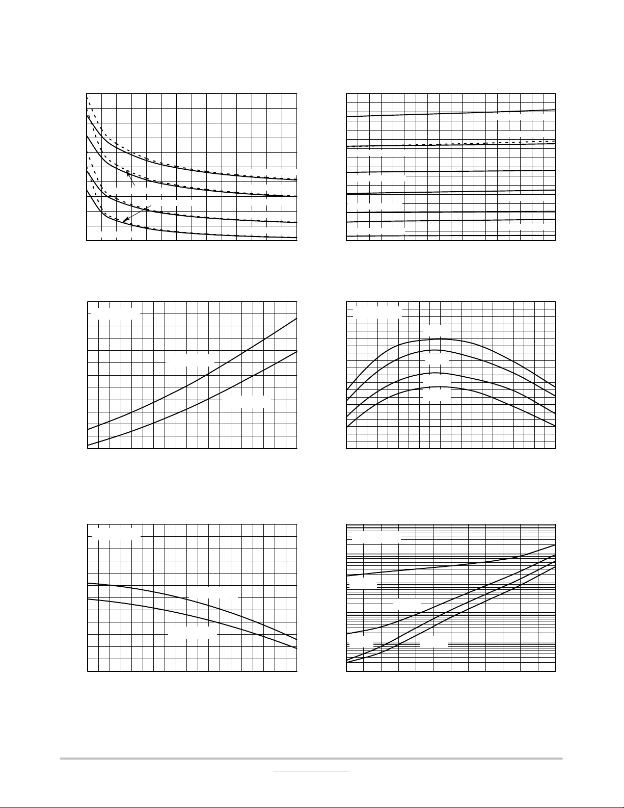
TYPICAL PERFORMANCE CURVES
10
(A)
Lmax
I
T
= 150°C
J(start)
1
10 100
T
J(start)
= 25°C
L (mH)
Figure 3. Single Pulse Maximum Switch−Off
Current vs. Load Inductance
10
(A)
Lmax
I
T
J(start)
= 150°C
T
J(start)
= 25°C
1000
T
= 25°C
J(start)
(mJ)
100
max
E
10
10 100
T
J(start)
= 150°C
L (mH)
Figure 4. Single Pulse Maximum Switching
Energy vs. Load Inductance
1000
T
= 25°C
J(start)
(mJ)
100
max
E
T
J(start)
= 150°C
1
110
tav (ms)
Figure 5. Single Pulse Maximum Inductive
Switch−Off Current vs. Time in Avalanche
12
10
TA = 25°C
6 V
7 V
9 V
10
110
tav (ms)
Figure 6. Single Pulse Maximum Inductive
Switching Energy vs. Time in Avalanche
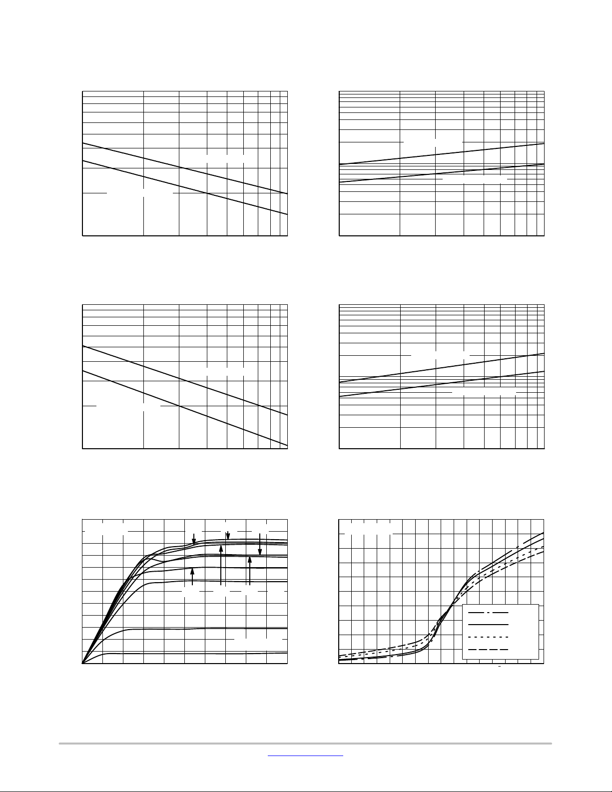
10
VDS = 10 V
8
8
6
(A)
D
I
6
10 V
8 V
4
2
0
0123 45
VGS = 2.5 V
VDS (V)
Figure 7. On−State Output Characteristics
5 V
4 V
3 V
(A)
D
I
4
2
0
1.5 2.5 3.5 4.5
12345
VGS (V)
Figure 8. Transfer Characteristics
−40°C
25°C
105°C
150°C
www.onsemi.com
4
Page 5
NCV8415
TYPICAL PERFORMANCE CURVES
300
250
200
(mW)
150
DS(ON)
R
100
50
105°C, ID = 1.4 A
−40°C, ID = 1.4 A
−40°C, ID = 0.5 A
345678910
150°C, ID = 1.4 A
150°C, ID = 0.5 A
105°C, ID = 0.5 A
25°C, ID = 1.4 A
25°C, ID = 0.5 A
VGS (V)
Figure 9. R
vs. Gate−Source Voltage
DS(ON)
2.0
ID = 1.4 A
1.75
1.5
DS(ON)
VGS = 5 V
1.25
1.0
VGS = 10 V
Normalized R
0.75
210
190
170
150
150°C, VGS = 10 V
(mW)
130
105°C, VGS = 10 V
DS(ON)
110
R
90
25°C, VGS = 10 V
70
−40°C, VGS = 10 V
50
0.2 0.4 0.6 0.8 1 1.2 1.4 1.6 1.8 2
150°C, VGS = 5 V
105°C, VGS = 5 V
25°C, VGS = 5 V
−40°C, VGS = 5 V
ID (A)
Figure 10. R
vs. Drain Current
DS(ON)
12
VDS = 10 V
11.5
11
−40°C
10.5
25°C
105°C
150°C
(A)
LIM
I
10
9.5
9
8.5
8
7.5
0.5
−40 −20 0 20 40 60 80 100 120 140 5 6 7 8 9 10
TJ (5C)
Figure 11. Normalized R
vs. Temperature
DS(ON)
7
5.5 6.5 7.5 8.5 9.5
VGS (V)
Figure 12. Current Limit vs. Gate−Source
Voltage
10
VDS = 10 V
9.5
9
(A)
8.5
LIM
I
VGS = 10 V
8
VGS = 5 V
7.5
7
−40 −20 0 20 40 60 80 100 120 140
TJ (5C)
Figure 13. Current Limit vs. Junction
Temperature
100
10
1
(mA)
DSS
0.1
I
0.01
0.001
www.onsemi.com
5
VGS = 0 V
150°C
105°C
25°C
−40°C
10 15 20 25 30 35 40
VDS (V)
Figure 14. Drain−to−Source Leakage Current
Page 6

NCV8415
TYPICAL PERFORMANCE CURVES
1.2
ID = 150 mA
= V
1.1
(V)
GS(th)
1
V
DS
GS
0.9
0.8
Normalized V
0.7
0.6
−40 −20 0 20 40 60 80 100 120 140
TJ (5C)
Figure 15. Normalized Threshold Voltage vs.
Temperature
140
VDD = 12 V
= 1 A
I
120
R
D
= 0 W
G
100
t
ON
80
60
Time (ms)
t
40
r
t
OFF
20
t
0
345678910
f
VGS (V)
Figure 17. Resistive Load Switching Time vs.
Gate−Source Voltage
1.1
VGS = 0 V
1
−40°C
0.9
0.8
0.7
25°C
105°C
(V)
SD
V
0.6
150°C
0.5
12345678910
IS (A)
Figure 16. Source−Drain Diode Forward
Characteristics
2
VDD = 12 V
= 1 A
I
D
R
= 0 W
1.5
G
−dVDS/dt
ON
1.0
dVDS/dt
OFF
0.5
Drain−Source Voltage Slope (V/ms)
0
345678910
VGS (V)
Figure 18. Resistive Load Switching
Drain−Source Voltage Slope vs. Gate−Source
Voltage
80
VDD = 12 V
70
60
50
I
D
= 1 A
t
, VGS = 10 V
OFF
t
, VGS = 5 V
OFF
40
Time (ms)
30
tON, VGS = 5 V
tr, VGS = 5 V
20
10
tf, VGS = 10 Vtf, VGS = 5 V
tON, VGS = 10 V
tr, VGS = 10 V
0
0 500 1000 1500 2000
RG (W)
Figure 19. Resistive Load Switching Time vs.
Gate Resistance
2
1.8
1.6
1.4
1.2
1
0.8
0.6
0.4
0.2
Drain−Source Voltage Slope (V/ms)
0
Drain−Source Voltage Slope vs. Gate Resistance
www.onsemi.com
6
−dVDS/dtON, VGS = 10 V
dVDS/dt
, VGS = 5 V
OFF
dVDS/dt
, VGS = 10 V
OFF
−dVDS/dtON, VGS = 5 V
VDD = 12 V
= 1 A
I
D
0 500 1000 1500 2000
RG (W)
Figure 20. Resistive Load Switching
Page 7

NCV8415
TYPICAL PERFORMANCE CURVES
100
90
80
70
(5C/W)
JA
q
R
60
50
PCB Cu thickness, 2.0 oz
40
0 100 200 300 400 500 600 700
PCB Cu thickness, 1.0 oz
Copper Heat Spreader Area (mm
Figure 21. R
vs. Copper Area (SOT−223)
q
JA
800
2
)
90
80
70
60
(5C/W)
JA
q
R
50
40
PCB Cu thickness, 2.0 oz
30
0 100 200 300 400 500 600 700
PCB Cu thickness, 1.0 oz
Copper Heat Spreader Area (mm
Figure 22. R
vs. Copper Area (DPAK)
q
JA
2
)
100
50% Duty Cycle
20% Duty Cycle
10
10% Duty Cycle
5% Duty Cycle
2% Duty Cycle
1
(t) (5C/W)
R
JA
q
1% Duty Cycle
0.1
Single Pulse
80 × 80 × 1.6 mm Single−Layer PCB, 645 mm2 1 oz. Copper
0.01
0.000001 0.00001 0.0001 0.001 0.01 0.1 1 10 100 1000
Pulse Width (s)
Figure 23. Transient Thermal Resistance (SOT−223)
800
100
50% Duty Cycle
20% Duty Cycle
10
10% Duty Cycle
5% Duty Cycle
2% Duty Cycle
1
(t) (5C/W)
JA
1% Duty Cycle
q
R
0.1
Single Pulse
80 × 80 × 1.6 mm Single−Layer PCB, 645 mm2 1 oz. Copper
0.01
0.000001 0.00001 0.0001 0.001 0.01 0.1 1 10 100 1000
Pulse Width (s)
Figure 24. Transient Thermal Resistance (DPAK)
www.onsemi.com
7
Page 8

NCV8415
APPLICATION INFORMATION
Circuit Protection Features
The NCV8415 has three main protections. Current Limit,
Thermal Shutdown and Delta Thermal Shutdown. These
protections establish robustness of the NCV8415.
Current Limit and Short Circuit Protection
The NCV8415 has current sense element. In the event that
the drain current reaches designed current limit level,
integrated Current Limit protection establishes its constant
level.
Delta Thermal Shutdown
Delta Thermal Shutdown (DTSD) Protection increases
higher reliability of the NCV8415. DTSD consist of two
independent temperature sensors – cold and hot sensors. The
NCV8415 establishes a slow junction temperature rise by
sensing the difference between the hot and cold sensors.
ON/OFF output cycling is designed with hysteresis that
results in a controlled saw tooth temperature profile
(Figure 26). The die temperature slowly rises (DTSD) until
the absolute temperature shutdown (TSD) is reached around
175°C.
Thermal Shutdown with Automatic Restart
Internal Thermal Shutdown (TSD) circuitry is provided to
protect the NCV8415 in the event that the maximum
junction temperature is exceeded. When activated at
typically 175°C, the NCV8415 turns off. This feature is
provided to prevent failures from accidental overheating.
EMC Performance
To improve the EMC performance/robustness, connect
a small ceramic capacitor to the drain pin as close to the
device as possible according to Figure 25.
R
L
Gate
D
DUT
G
S
Figure 25. EMC Capacitor Placement
+
V
DD
−
C
V
Delta TSD
activation
G
I
D
I
NOM
TSD
T
TEST CIRCUITS AND WAVEFORMS
Thermal Transient Limitation Phase Overtemperature
I
LIM
J
Cycling
Nominal
Load
Time
Figure 26. Overload Protection Behavior
www.onsemi.com
8
Page 9

NCV8415
TEST CIRCUITS AND WAVEFORMS
R
L
V
IN
R
G
D
DUT
G
S
I
DS
Figure 27. Resistive Load Switching Test Circuit
+
V
DD
−
90%
V
IN
10%
t
ON
t
r
t
OFF
t
f
90%
I
DS
10%
Time
Figure 28. Resistive Load Switching Waveforms
www.onsemi.com
9
Page 10

NCV8415
TEST CIRCUITS AND WAVEFORMS
L
V
DS
V
IN
R
G
G
DUT
S
t
p
I
DS
D
+
V
DD
−
Figure 29. Inductive Load Switching Test Circuit
5 V
V
IN
t
V
(BR)DSS
av
V
DD
t
p
I
pk
V
DS
0 V
V
I
DS
DS(on)
0
Time
Figure 30. Inductive Load Switching Waveforms
www.onsemi.com
10
Page 11

MECHANICAL CASE OUTLINE
PACKAGE DIMENSIONS
SCALE 1:1
SOT−223 (TO−261)
CASE 318E−04
ISSUE R
DATE 02 OCT 2018
q
q
DOCUMENT NUMBER:
DESCRIPTION:
ON Semiconductor and are trademarks of Semiconductor Components Industries, LLC dba ON Semiconductor or its subsidiaries in the United States and/or other countries.
ON Semiconductor reserves the right to make changes without further notice to any products herein. ON Semiconductor makes no warranty, representation or guarantee regarding
the suitability of its products for any particular purpose, nor does ON Semiconductor assume any liability arising out of the application or use of any product or circuit, and specifically
disclaims any and all liability, including without limitation special, consequential or incidental damages. ON Semiconductor does not convey any license under its patent rights nor the
rights of others.
98ASB42680B
SOT−223 (TO−261)
Electronic versions are uncontrolled except when accessed directly from the Document Repository.
Printed versions are uncontrolled except when stamped “CONTROLLED COPY” in red.
PAGE 1 OF 2
© Semiconductor Components Industries, LLC, 2018
www.onsemi.com
Page 12

SOT−223 (TO−261)
CASE 318E−04
ISSUE R
DATE 02 OCT 2018
STYLE 1:
PIN 1. BASE
2. COLLECTOR
3. EMITTER
4. COLLECTOR
STYLE 6:
PIN 1. RETURN
2. INPUT
3. OUTPUT
4. INPUT
STYLE 11:
PIN 1. MT 1
2. MT 2
3. GATE
4. MT 2
STYLE 2:
PIN 1. ANODE
2. CATHODE
3. NC
4. CATHODE
STYLE 7:
PIN 1. ANODE 1
2. CATHODE
3. ANODE 2
4. CATHODE
STYLE 12:
PIN 1. INPUT
2. OUTPUT
3. NC
4. OUTPUT
STYLE 3:
PIN 1. GATE
STYLE 8:
STYLE 13:
PIN 1. GATE
2. DRAIN
3. SOURCE
4. DRAIN
CANCELLED
2. COLLECTOR
3. EMITTER
4. COLLECTOR
GENERIC
MARKING DIAGRAM*
AYW
XXXXXG
G
1
A = Assembly Location
Y = Year
W = Work Week
XXXXX = Specific Device Code
G = Pb−Free Package
(Note: Microdot may be in either location)
*This information is generic. Please refer to
device data sheet for actual part marking.
Pb−Free indicator, “G” or microdot “G”, may
or may not be present. Some products may
not follow the Generic Marking.
STYLE 4:
PIN 1. SOURCE
2. DRAIN
3. GATE
4. DRAIN
STYLE 9:
PIN 1. INPUT
2. GROUND
3. LOGIC
4. GROUND
STYLE 5:
PIN 1. DRAIN
2. GATE
3. SOURCE
4. GATE
STYLE 10:
PIN 1. CATHODE
2. ANODE
3. GATE
4. ANODE
DOCUMENT NUMBER:
DESCRIPTION:
ON Semiconductor and are trademarks of Semiconductor Components Industries, LLC dba ON Semiconductor or its subsidiaries in the United States and/or other countries.
ON Semiconductor reserves the right to make changes without further notice to any products herein. ON Semiconductor makes no warranty, representation or guarantee regarding
the suitability of its products for any particular purpose, nor does ON Semiconductor assume any liability arising out of the application or use of any product or circuit, and specifically
disclaims any and all liability, including without limitation special, consequential or incidental damages. ON Semiconductor does not convey any license under its patent rights nor the
rights of others.
© Semiconductor Components Industries, LLC, 2018
98ASB42680B
SOT−223 (TO−261)
Electronic versions are uncontrolled except when accessed directly from the Document Repository.
Printed versions are uncontrolled except when stamped “CONTROLLED COPY” in red.
PAGE 2 OF 2
www.onsemi.com
Page 13

MECHANICAL CASE OUTLINE
PACKAGE DIMENSIONS
2
1
3
SCALE 1:1
L3
L4
b2
e
GAUGE
L2
PLANE
STYLE 1:
PIN 1. BASE
2. COLLECTOR
3. EMITTER
4. COLLECTOR
STYLE 6:
PIN 1. MT1
2. MT2
3. GATE
4. MT2
4
E
b3
4
12 3
TOP VIEW
L
L1
DETAIL A
ROTATED 90 CW5
STYLE 7:
PIN 1. GATE
2. COLLECTOR
3. EMITTER
4. COLLECTOR
5.80
0.228
A
A
B
D
NOTE 7
b
0.005 (0.13) C
DETAIL A
c
SIDE VIEW
M
H
SEATING
C
PLANE
A1
STYLE 2:
PIN 1. GATE
2. DRAIN
3. SOURCE
4. DRAIN
STYLE 8:
PIN 1. N/C
2. CATHODE
3. ANODE
4. CATHODE
STYLE 3:
PIN 1. ANODE
2. CATHODE
3. ANODE
4. CATHODE
SOLDERING FOOTPRINT*
6.20
0.244
2.58
0.102
3.00
0.118
1.60
0.063
DPAK (SINGLE GAUGE)
CASE 369C
ISSUE F
C
c2
H
BOTTOM VIEW
Z
BOTTOM VIEW
ALTERNATE
CONSTRUCTIONS
STYLE 4:
PIN 1. CATHODE
2. ANODE
3. GATE
4. ANODE
STYLE 9:
PIN 1. ANODE
2. CATHODE
3. RESISTOR ADJUST
4. CATHODE
6.17
0.243
STYLE 10:
STYLE 5:
PIN 1. GATE
2. ANODE
3. CATHODE
4. ANODE
PIN 1. CATHODE
2. ANODE
3. CATHODE
4. ANODE
DATE 21 JUL 2015
NOTES:
1. DIMENSIONING AND TOLERANCING PER ASME
Y14.5M, 1994.
2. CONTROLLING DIMENSION: INCHES.
3. THERMAL PAD CONTOUR OPTIONAL WITHIN DIMENSIONS b3, L3 and Z.
4. DIMENSIONS D AND E DO NOT INCLUDE MOLD
FLASH, PROTRUSIONS, OR BURRS. MOLD
FLASH, PROTRUSIONS, OR GATE BURRS SHALL
Z
Z
NOT EXCEED 0.006 INCHES PER SIDE.
5. DIMENSIONS D AND E ARE DETERMINED AT THE
OUTERMOST EXTREMES OF THE PLASTIC BODY.
6. DATUMS A AND B ARE DETERMINED AT DATUM
PLANE H.
7. OPTIONAL MOLD FEATURE.
DIM MIN MAX MIN MAX
A 0.086 0.094 2.18 2.38
A1 0.000 0.005 0.00 0.13
b 0.025 0.035 0.63 0.89
b2 0.028 0.045 0.72 1.14
b3 0.180 0.215 4.57 5.46
c 0.018 0.024 0.46 0.61
c2 0.018 0.024 0.46 0.61
D 0.235 0.245 5.97 6.22
E 0.250 0.265 6.35 6.73
e 0.090 BSC 2.29 BSC
H 0.370 0.410 9.40 10.41
L 0.055 0.070 1.40 1.78
L1 0.114 REF 2.90 REF
L2 0.020 BSC 0.51 BSC
L3 0.035 0.050 0.89 1.27
L4 −−− 0.040 −−− 1.01
Z 0.155 −−− 3.93 −−−
MILLIMETERSINCHES
GENERIC
MARKING DIAGRAM*
XXXXXXG
ALYWW
XXXXXX = Device Code
A = Assembly Location
L = Wafer Lot
Y = Year
WW = Work Week
G = Pb−Free Package
*This information is generic. Please refer
to device data sheet for actual part
marking.
AYWW
XXX
XXXXXG
DiscreteIC
mm
ǒ
SCALE 3:1
inches
Ǔ
*For additional information on our Pb−Free strategy and soldering
details, please download the ON Semiconductor Soldering and
Mounting Techniques Reference Manual, SOLDERRM/D.
DOCUMENT NUMBER:
DESCRIPTION:
ON Semiconductor and are trademarks of Semiconductor Components Industries, LLC dba ON Semiconductor or its subsidiaries in the United States and/or other countries.
ON Semiconductor reserves the right to make changes without further notice to any products herein. ON Semiconductor makes no warranty, representation or guarantee regarding
the suitability of its products for any particular purpose, nor does ON Semiconductor assume any liability arising out of the application or use of any product or circuit, and specifically
disclaims any and all liability, including without limitation special, consequential or incidental damages. ON Semiconductor does not convey any license under its patent rights nor the
rights of others.
© Semiconductor Components Industries, LLC, 2018
98AON10527D
DPAK (SINGLE GAUGE)
Electronic versions are uncontrolled except when accessed directly from the Document Repository.
Printed versions are uncontrolled except when stamped “CONTROLLED COPY” in red.
PAGE 1 OF 1
www.onsemi.com
Page 14

ON Semiconductor and are trademarks of Semiconductor Components Industries, LLC dba ON Semiconductor or its subsidiaries in the United States and/or other countries.
ON Semiconductor owns the rights to a number of patents, trademarks, copyrights, trade secrets, and other intellectual property. A listing of ON Semiconductor’s product/patent
coverage may be accessed at www.onsemi.com/site/pdf/Patent−Marking.pdf
ON Semiconductor makes no warranty, representation or guarantee regarding the suitability of its products for any particular purpose, nor does ON Semiconductor assume any liability
arising out of the application or use of any product or circuit, and specifically disclaims any and all liability, including without limitation special, consequential or incidental damages.
Buyer is responsible for its products and applications using ON Semiconductor products, including compliance with all laws, regulations and safety requirements or standards,
regardless of any support or applications information provided by ON Semiconductor. “Typical” parameters which may be provided in ON Semiconductor data sheets and/or
specifications can and do vary in different applications and actual performance may vary over time. All operating parameters, including “Typicals” must be validated for each customer
application by customer’s technical experts. ON Semiconductor does not convey any license under its patent rights nor the rights of others. ON Semiconductor products are not
designed, intended, or authorized for use as a critical component in life support systems or any FDA Class 3 medical devices or medical devices with a same or similar classification
in a foreign jurisdiction or any devices intended for implantation in the human body. Should Buyer purchase or use ON Semiconductor products for any such unintended or unauthorized
application, Buyer shall indemnify and hold ON Semiconductor and its officers, employees, subsidiaries, affiliates, and distributors harmless against all claims, costs, damages, and
expenses, and reasonable attorney fees arising out of, directly or indirectly, any claim of personal injury or death associated with such unintended or unauthorized use, even if such
claim alleges that ON Semiconductor was negligent regarding the design or manufacture of the part. ON Semiconductor is an Equal Opportunity/Affirmative Action Employer. This
literature is subject to all applicable copyright laws and is not for resale in any manner.
. ON Semiconductor reserves the right to make changes without further notice to any products herein.
PUBLICATION ORDERING INFORMATION
LITERATURE FULFILLMENT:
Email Requests to: orderlit@onsemi.com
ON Semiconductor Website: www.onsemi.com
TECHNICAL SUPPORT
North American Technical Support:
Voice Mail: 1 800−282−9855 Toll Free USA/Canada
Phone: 011 421 33 790 2910
Europe, Middle East and Africa Technical Support:
Phone: 00421 33 790 2910
For additional information, please contact your local Sales Representative
◊
www.onsemi.com
1
 Loading...