

Page 1
USB Power Delivery
4-Switch Buck Boost
Controller
NCV81599, NCP81599
The NCV81599 USB Power Delivery (PD) Controller is a
synchronous buck boost that is optimized for converting battery
voltage or adaptor voltage into power supply rails required in
notebook, tablet, and desktop systems, as well as many other
consumer devices using USB PD standard and C−Type cables. The
NCV81599 is fully compliant to the USB Power Delivery
Specification when used in conjunction with a USB PD or C−Type
Interface Controller. NCV81599 is designed for applications requiring
dynamically controlled slew rate limited output voltage that require
either voltage higher or lower than the input voltage. The NCV81599
drives 4 NMOSFET switches, allowing it to buck or boost and support
the functions specified in the USB Power Delivery Specification
which is suitable for all USB PD applications. The USB PD Buck
Boost Controller operates with a supply and load range of 4.5 V to
32 V.
Features
• Wide Input Voltage Range:
from 4.5 V to 32 V for NCV81599
from 4.5 V to 28 V for NCP81599
• Dynamically Programmed Frequency from 150 kHz to 1.2 MHz
2
• I
C Interface
• Real Time Power Good Indication
• Controlled Slew Rate Voltage Transitioning
• Feedback Pin with Internally Programmed Reference
• Support USBPD/QC2.0/QC3.0 Profile
• 2 Independent Current Sensing Inputs
• Over Temperature Protection
• Adaptive Non−Overlap Gate Drivers
• Over−Voltage and Over−Current Protection
• AEC−Q100 Qualified (NCV81599)
• 5 x 5 mm QFN32 Package
www.onsemi.com
32
1
QFN32 5x5, 0.5P
CASE 485CE
(NCP81599)
MARKING DIAGRAM
1
NCx81599
AWLYYWWG
G
NCx81599 = Specific Device Code
x = V or P
A = Assembly Location
WL = Wafer Lot
YY = Year
WW = Work Week
G = Pb−Free Package
(Note: Microdot may be in either location)
Typical Application
1
QFNW32 5x5, 0.5P
CASE 484AB
(NCV81599)
• Automotive USB Charging Ports
• Wireless Charging
• Consumer Electronics
32
ORDERING INFORMATION
Device Package Shipping
NCV81599MWTXG QFN32
(Pb−Free)
NCP81599MNTXG QFN32
(Pb−Free)
†For information on tape and reel specifications, including part orientation
and tape sizes, please refer to our Tape and Reel Packaging Specification
Brochure, BRD8011/D.
© Semiconductor Components Industries, LLC, 2017
March, 2021 − Rev. 3
5000 / Tape & Reel
2500 / Tape & Reel
†
1 Publication Order Number:
NCV81599/D
Page 2
R
VCCD
Current Sense 1
Current Sense 2
Curret Limit Indicator
R
ADDR
C
VCCD
R
DRV
Interrupt
Enable
I2C
CP
NCV81599, NCP81599
V1
RS2
CB2
V2
Q6
VBUS
RPU
CO1
RPD
S4
S3
VCCD
C
VDRV
VDRV
VCC
C
VCC
CS1
R
CS1
CS2
R
CS2
CLIND
INT
EN
SDA
SCL
ADDR
COMP
RC
AGND
CC
THPAD
CSP1
CSN1
CSN2
CSP2
BST2
BST1
HSG1
VSW1
HSG2
VSW2
LSG1
PGND1
LSG2
PGND2
PDRV
V1
RS1
FB
V2
S1
S2
CB1
L1
HSG1
LSG1
PGND1
CSN1
CSP1
V1
CS1
CLIND
Figure 1. Typical Application Circuit
VSW1
BST1
VCC
VDRV
31 30 29 28 27 26 2532
1
2
3
4
Exposed Thermal Pad
5
(THPAD)
6
7
8
INT
SCL
SDA
ADDR
VCCD
AGND
V2
AGND
VSW2
1514131211109 16
COMP
BST2
EN
24
23
22
21
20
19
18
17
HSG2
LSG2
PGND2
CSP2
CSN2
FB
CS2
PDRV
Figure 2. Pinout
www.onsemi.com
2
Page 3
NCV81599, NCP81599
ADDR
VCC
VDRV
V2
CS1
CS2
CLIND
EN
VCCD
SDA
SCL
INT
COMP
CONFIG
VDRV
CS1
CLIMP1
CLIMP2
CS2
CLIND
0.8V
CONFIG
4.0V
VCC
−
+
I2C ADDR
SETTING
4.0V
+
−
−
+
I2C
Interface
Interface
AGND
+
−
Startup
INPUT
UVLO
+
−
EN_MASK
EN_INT
EN
LOGIC
INT
Vcc_rdy
V1
BG
OV2_th
CLINDP1
CLINDP2
EN
Value
Register
Configuration
Registers
PG
TS
VDRV_rdy
+
−
CLIND
ADC
Digital
Status
THPAD
PDRV
V2_OVLO
Analog
Mux
Registers
Master OSC
Oscillator
Reference
VFB
CONFIG
FB
V1
CS1
CS2
Limit
0_Ramp
OCP
logic
VFB
PG_High
VFB
Ramp_0
Ramp_180
BG
Error OTA
500μS/100μS
+
_
SW1
SW2
SW3
SW4
PG
TS
CLIND
PG_Low
OV_REF
CS2_INT
CS1_INT
EN
−
+
−
+
+
−
∑
∑
BG
Shutdown
TS
Boot1 _UVLO
Control
Logic
LOGIC
0_Ramp
CS1_INT
CS2_INT
CS1_INT
180_Ramp
−
+
−
+
v1_OVLO
Thermal
OV_MSK
PG_MSK
OV
PG/
OV/
PG
CONFIG
V1
CSP1
CS1
CS1_INT
Logic_1
Drive
Logic_2
Boot2 _UVLO
CS2
CS2_INT
CSN2
+
Boot1V
NOL
Drive
NOL
Buck Logic
Boost Logic
Buck Boost
Logic
VFB
+
VDRV
VDRV
+
VDRV
SW1
SW4
_
OV1_th
V1
CSP1
+
_
CSN1
BST1
HSG1
VSW1
LSG1
PGND1
PGND2
LSG2
VSW2
HSG2
BST2
Boot2 V
+
_
CSP2
CSN2
PDRV
SW2
SW3
FB
Figure 3. Block Diagram
www.onsemi.com
3
Page 4

NCV81599, NCP81599
Table 1. PIN FUNCTION DESCRIPTION
Pin Pin Name Description
1 HSG1 S1 gate drive. Drives the S1 N−channel MOSFET with a voltage equal to VDRV superimposed on the switch
2 LSG1 Drives the gate of the S2 N−channel MOSFET between ground and VDRV.
3, 22 PGND Power ground for the low side MOSFET drivers. Connect these pins closely to the source of the bottom
4 CSN1 Negative terminal of the current sense amplifier.
5 CSP1 Positive terminal of the current sense amplifier.
6 V1 Input voltage of the converter
7 CS1 Current sense amplifier output. CS1 will source a current that is proportional to the voltage across RS1 to an
8 CLIND Open drain output, high voltage on CLIND pin indicates that the CS1 or CS2 voltage has exceeded the I2C
9 SDA I2C interface data line.
10 SCL I2C interface clock line.
11 INT Interrupt is an open drain output that indicates the state of the output power, the internal thermal trip, and oth-
12 ADDR
13−14 AGND The ground pin for the analog circuitry.
15 COMP Output of the transconductance amplifier used for stability in closed loop operation.
16 EN Logic high enables the switching and logic low shuts down and reset the device. Middle level makes the de-
17 PDRV The open drain output used to control a PMOSFET.
18 CS2 Current sense amplifier output. CS2 will source a current that is proportional to the voltage across RS2 to an
19 FB Feedback voltage of the output, negative terminal of the gm amplifier.
20 CSN2 Negative terminal of the current sense amplifier.
21 CSP2 Positive terminal of the current sense amplifier.
23 LSG2 Drives the gate of the S3 N−channel MOSFET between ground and VDRV.
24 HSG2 S4 gate drive. Drives the S4 N−channel MOSFET with a voltage equal to VDRV superimposed on the switch
25 BST2 Bootstrapped Driver Supply. The BST2 pin swings from a forward voltage drop below VDRV up to a forward
26 VSW2 Switch Node. VSW2 pin swings from a diode voltage drop below ground up to output voltage.
27 V2 Output voltage of the converter. Connect to the output externally for OVLO sense.
28 VCCD
29 VDRV
30 VCC The VCC pin supplies power to the internal circuitry. The VCC is the output of a linear regulator which is pow-
31 VSW1 Switch Node. VSW1 pin swings from a diode voltage drop below ground up to V1.
32 BST1 Bootstrapped Driver Supply. The BST1 pin swings from a forward voltage drop below VDRV up to a forward
33 THPAD Center Thermal Pad. Connect to AGND externally.
node voltage VSW1.
N−channel MOSFETs.
external resistor. CS1 voltage can be monitored with a high impedance input. Ground this pin if not used.
programmed limit.
2
er I
C programmable functions.
I2C address pin, placing a less than 200 kW resistor to the ground to set the I2C address.
vice to stop switching and keep the VCC alive.
external resistor. CS2 voltage can be monitored with a high impedance input. Ground this pin if not used.
node voltage VSW2.
voltage drop below VOUT + VDRV. Place a 0.1 mF capacitor from this pin to VSW2.
Internal digital power supply input. Always connect VCCD to VCC. A 1 mF capacitor should be placed close to
the part to decouple this line.
Internal voltage supply to the driver circuits. A 1 mF capacitor should be placed close to the part to decouple
this line.
ered from V1. Pin should be decoupled with a 1 mF capacitor for stable operation.
voltage drop below V1 + VDRV. Place a 0.1 mF capacitor from this pin to VSW1.
www.onsemi.com
4
Page 5
NCV81599, NCP81599
Table 2. MAXIMUM RATINGS
Over operating free−air temperature range unless otherwise noted
Rating
VCCD Input Voltage VCCD −0.3 5.5 V
Address Pin Output Voltage ADDR −0.3 5.5 V
Driver Input Voltage VDRV −0.3 5.5 V
Internal Regulator Output VCC −0.3 5.5 V
Output of Current Sense Amplifiers CS1, CS2 −0.3 5.5 V
Current Limit Indicator CLIND −0.3 VCC + 0.3 V
Interrupt Indicator INT −0.3 VCC + 0.3 V
Enable Input EN −0.3 5.5 V
I2C Communication Lines SDA, SCL −0.3 VCC + 0.3 V
Compensation Output COMP −0.3 VCC + 0.3 V
V1 Power Stage Input Voltage V1 −0.3 35 V, 40 V (20 ns) V
Positive Current Sense CSP1 −0.3 35 V, 40 V (20 ns) V
Negative Current Sense CSN1 −0.3 35 V, 40 V (20 ns) V
Positive Current Sense CSP2 −0.3 35 V, 40 V (20 ns) V
Negative Current Sense CSN2 −0.3 35 V, 40 V (20 ns) V
Feedback Voltage FB −0.3 5.5 V
Driver 1 and Driver 2 Positive Rails BST1,
High Side Driver 1 and Driver 2 HSG1,
Switching Nodes and Return Path of Driver 1 and Driver 2 VSW1, VSW2 −2.0 V,
Low Side Driver 1 and Driver 2 LSG1, LSG2 −0.3 V 5.5 V
PMOSFET Driver PDRV −0.3 35 V, 40 V (20 ns) V
Voltage Differential AGND to PGND −0.3 0.3 V
CSP1−CSN1, CSP2−CSN2 Differential Voltage CS1DIF, CS2DIF −0.5 0.5 V
PDRV Maximum Current PDRVI 0 10 mA
PDRV Maximum Pulse Current
(100 ms on time, with > 1 s interval)
Maximum VCC Current VCCI 0 mA
Operating Junction Temperature Range (Note 1) TJ −40 150 °C
Operating Ambient Temperature Range TA −40 125 °C
Storage Temperature Range TSTG −55 150 °C
Thermal Characteristics (Note 2)
QFN 32 5mm x 5mm
Maximum Power Dissipation @ TA = 25°C
Maximum Power Dissipation @ TA = 85°C
Thermal Resistance Junction−to−Air with Solder
Thermal Resistance Junction−to−Case Top with Solder
Thermal Resistance Junction−to−Case Bottom with Solder
Lead Temperature Soldering (10 sec):
Reflow (SMD styles only) Pb−Free (Note 3)
Stresses exceeding those listed in the Maximum Ratings table may damage the device. If any of these limits are exceeded, device functionality
should not be assumed, damage may occur and reliability may be affected.
1. The maximum package power dissipation limit must not be exceeded.
2. The value of QJA is measured with the device mounted on a 3in x 3in, 4 layer, 0.062 inch FR−4 board with 1.5 oz. copper on the top and
bottom layers and 0.5 ounce copper on the inner layers, in a still air environment with T
3. 60−180 seconds minimum above 237°C.
Symbol Min Max Unit
−0.3 V wrt/PGND
BST2
HSG2
PDRVIPUL 0 200 mA
PD
PD
RQJA
RQJCT
RQJCB
RF 260 Peak °C
−0.3 V wrt/VSW
−0.3 V wrt/PGND
−0.3 V wrt/VSW
−5 V (100 ns)
4.1
2.1
30
1.7
2.0
A = 25°C.
40 V
5.5 V wrt/VSW
40 V
5.5 V wrt/VSW
35 V, 40 V (20 ns) V
°C/W
°C/W
°C/W
V
V
W
W
www.onsemi.com
5
Page 6
NCV81599, NCP81599
Table 3. ELECTRICAL CHARACTERISTICS
= 12 V, V
(V1
= 5 V , T
out
Parameter
POWER SUPPLY
V1 Operating Input Voltage V1
VDRV Operating Input Voltage VDRV 4.5 5 5.5 V
VCCD Operating Input Voltage VCCD 4.5 5.5 V
VCC UVLO Rising Threshold VCC
VCC UVLO Falling Threshold VCC
UVLO Hysteresis for VCC VCCV
VDRV UVLO Rising Threshold VDRV
VDRV UVLO Falling Threshold VDRV
VDRV UVLO Hysteresis VDRV
VCC Output Voltage VCC With no external load 4.5 5 V
VCC Drop Out Voltage VCCDROOP 30 mA load 100 mV
VCC Output Current Limit IOUT
VCC Short Current Limit IVCC_SHORT VCC short 14.6 mA
V1 Shutdown Supply Current IVCC_SD EN < 0.4 V, V1 = 12 V 8.0 15
V1 Normal Current IV1 0.8 V < EN < 1.88 V, 4.5 V ≤ V1 ≤
VCCD Standby Current IVCCD 0.8 V < EN < 1.88 V 4 mA
VCCD Switching Current IVCCD_SW EN > 2.2 V 4.1 mA
VDRIVE Switching Current Buck IV1_SW EN = 5 V, Cgate = 2.2 nF,
VDRIVE Switching Current Boost IV1_SW EN = 5 V, Cgate = 2.2 nF,
VOLTAGE OUTPUT
Voltage Output Accuracy
Voltage Accuracy Over Temperature
TRANSCONDUCTANCE AMPLIFIER
Gain Bandwidth Product
Transconductance GM1 Default 500
Max Output Source Current limit GMSOC 60 80
Max Output Sink Current limit GMSIC 60 80
Voltage Ramp Vramp 1.2 V
INTERNAL BST SWITCH
Pass FET Rds(on)
Reverse Leakage Current from BST
pin to VDRV pin
BST−VSW UVLO BST
BST−VSW UVLO BST
4. Ensured by design. Not production tested.
5. Typical value only. Not production tested.
= +25°C for typical value; −40°C < T
A
Symbol Test Conditions Min Typ Max Units
RISE
FALL
HYS
RISE
FALL
HYS
VCC
FB DAC_TARGET = 00110010
VOUTERT VFB ≥ 0.5 V
VOUTER T
GBW (Note 4) 5.2 MHz
RBST IF = 1 mA 60
DIL BST = 32 V, T
_UVLO
_UVLO
= TJ < 125°C for min/max values unless noted otherwise)
A
NCV81599 4.5 32
NCP81599 4.5 28
4.21 4.27 4.35 V
3.90 3.96 4.06 V
Falling Hysteresis 300 mV
4.21 4.31 4.35 V
3.90 4.01 4.06 V
300 mV
VCC Loaded to 4.3 V, EN > 0.8 V 80 97 mA
mA
7.3 mA
32 V, (No Switching)
16 mA
VSW = 0 V, FSW = 600 kHz
15 mA
VSW = 0 V, FSW = 600 kHz
DAC_TARGET = 01111000
DAC_TARGET = 11001000
1.188
1.98
−1.0
0.495
VFB < 0.5 V
= 25°C
A
VFB ≥ 0.5 V −0.45 0.45
−5
0.5
1.2
2.0
0.505
1.212
2.02
1.0
5
mV
mS
mA
mA
= 25°C 0.05 1
A
mA
Falling 3.2 3.5 3.8 V
Rising 3.4 3.7 4.1 V
V
V
%
%
W
www.onsemi.com
6
Page 7
NCV81599, NCP81599
Table 3. ELECTRICAL CHARACTERISTICS (continued)
= 12 V, V
(V1
= 5 V , T
out
Parameter UnitsMaxTypMinTest ConditionsSymbol
INTERNAL BST SWITCH
BST−VSW Hysteresis
OSCILLATOR
Oscillator Frequency
Oscillator Frequency Accuracy FSWE −12 12 %
Minimum On Time MOT Measured at 10% to 90% of VCC (Note 4) 100 ns
Minimum Off Time MOFT Measured at 90% to 10% of VCC (Note 4) 100 ns
INT THRESHOLDS
Interrupt Low Voltage
Interrupt High Leakage Current INII 5 V 3 100 nA
Interrupt Startup Delay INTPG Soft Start end to PG positive edge 2.1 ms
Interrupt Propagation Delay
Power Good Threshold
FB Overvoltage Threshold FB_OV 115 %
Overvoltage Propagation Delay VFB_OVDL 1 Cycle
EXTERNAL CURRENT SENSE (CS1,CS2)
Positive Current Measurement High
Transconductance Gain Factor CSGT Current Sense Transconductance
Transconductance Deviation CSGE
Input Current Sense Common Mode
Range
Output Current Sense Common Mode
Range
Input Sense Voltage Full Scale ISVFS (Note 4) 100 mV
CS Output Voltage Range CSOR VSENSE = 100 mV Rset = 6k (Note 4) 0 3 V
EXTERNAL CURRENT LIMIT (CLIND)
Current Limit Indicator Output Low
Current Limit Indicator Output High
Leakage Current
INTERNAL CURRENT SENSE
Internal Current Sense Gain for PWM
4. Ensured by design. Not production tested.
5. Typical value only. Not production tested.
= +25°C for typical value; −40°C < T
A
BST
_HYS
FSW_0
VINTI IINT(sink) = 2 mA 0.2 V
PGI Delay for power good in 3.3 ms
PGO Delay for power good out 100 ns
PGTH Power Good in from falling
PGTH Power Good out from rising
CS10 CSP1−CSN1 or CSP2−CSN2 = 25 mV 125
CSCMMR_I CSP1 is tied to V1 4.5 32 V
CSCMMR_O 4 25.5 V
CLINDL
ICLINDH Pull up to 5 V 65 100 nA
ICG CSPx−CSNx = 25 mV 9.4 10 10.5 V/V
= TJ < 125°C for min/max values unless noted otherwise)
A
(Note 4) 200 mV
FSW = 001 (Note 5) 150
FSW = 000, default 552 600 648
FSW = 010 300
FSW = 011 450
FSW = 100 740
FSW = 101 880
FSW = 110 1145
104
Power Good out from falling
93
106
Power Good in from rising
95
5 mS
Vsense = 10 mV to 100 mV
CSPx−CSNx = 10 mV −30 30
CSPx−CSNx = 25 mV to 100 mV −20 20
Input current = 500 mA
7.0 100 mV
kHz
%
%
mA
%
www.onsemi.com
7
Page 8
NCV81599, NCP81599
Table 3. ELECTRICAL CHARACTERISTICS (continued)
= 12 V, V
(V1
= 5 V , T
out
Parameter UnitsMaxTypMinTest ConditionsSymbol
INTERNAL CURRENT SENSE
Positive Peak Current Limit Trip
Positive Peak Current Limit Latch−off OCP_L CLIP = 00 (default)
Negative Valley Current Limit Trip NVCLT CLIN = 00 (default)
SWITCHING MOSFET DRIVERS
HSG1 Pullup Resistance
HSG1 Pulldown Resistance HSG1_PD BST−VSW = 5 V 0.8
LSG1 Pullup Resistance LSG1_PU LSG −PGND = 5 V 2.4
LSG1 Pulldown Resistance LSG1_PD LSG −PGND = 5 V 0.7
HSG2 Pullup Resistance HSG2_PU BST−VSW = 5 V 2.7
HSG2 Pulldown Resistance HSG2_PD BST−VSW = 5 V 0.9
LSG2 Pullup Resistance LSG2_PU LSG −PGND = 5 V 2.0
LSG2 Pulldown Resistance LSG2_PD LSG −PGND = 5 V 0.7
HSG1 Falling to LSG1 Rising Delay HSLSD1 16 ns
LSG1 Falling to HSG1 Rising Delay LSHSD1 36 ns
HSG2 Falling to LSG2 Rising Delay HSLSD2 35 ns
LSG2 Falling to HSG2 Rising Delay LSHSD2 56 ns
SLEW RATE/SOFT START
Charge Slew Rate
(VOUT measured at V2 pin)
Discharge Slew Rate
(VOUT measured at V2 pin)
ENABLE
EN LDO High Threshold Voltage
EN LDO Low Threshold Voltage ENLDOLT 530 570 mV
EN Switching High Threshold Voltage ENHT 2.15 V
EN Switching Low Threshold Voltage ENLT 1.65 1.87 V
EN Pull Up Current (Default on) IEN_UP EN = 0.8 V 3.0
ADDR
Internal Current Source
ADDR0 ADDR = 74 H 110 mV
ADDR1 ADDR = 75 H 220 260 300 mV
ADDR2 ADDR = 76 H 380 440 500 mV
ADDR3 ADDR = 77 H 600 715 830 mV
4. Ensured by design. Not production tested.
5. Typical value only. Not production tested.
= +25°C for typical value; −40°C < T
A
PPCLT CLIP = 00 (default)
HSG1_PU BST−VSW = 5 V 2
SLEWP Slew = 00, FB = 0.1 VOUT
SLEWN Slew = 00, FB = 0.1 VOUT
ENLDOHT 770 810 mV
IADDR 9 10 11
= TJ < 125°C for min/max values unless noted otherwise)
A
34 39
CLIP = 01
CLIP = 10
CLIP = 11
CLIP = 01
CLIP = 10
CLIP = 11
34 40
CLIN = 01
CLIN = 10
CLIN = 11
Slew = 01, FB = 0.1 VOUT
Slew = 10, FB = 0.1 VOUT
Slew = 11, FB = 0.1 VOUT
Slew = 01, FB = 0.1 VOUT
Slew = 10, FB = 0.1 VOUT
Slew = 11, FB = 0.1 VOUT
23
44 mV
11
70
70
39
23
106
45 mV
25
15
0
0.6
1.2
2.4
4.8
−0.6
−1.2
−2.4
−4.8
mV
W
W
W
W
W
W
W
W
mV/ms
mV/ms
mA
mA
www.onsemi.com
8
Page 9
NCV81599, NCP81599
Table 3. ELECTRICAL CHARACTERISTICS (continued)
= 12 V, V
(V1
= 5 V , T
out
Parameter UnitsMaxTypMinTest ConditionsSymbol
I2C INTERFACE
Voltage Threshold Rising
Voltage Threshold Falling I2CVTH_F 0.9 V
Communication Speed I2CSP 1 MHz
THERMAL SHUTDOWN
Thermal Shutdown Threshold
Thermal Shutdown Hysteresis TSDHYS (Note 4) 28 °C
PDRV
PDRV Operating Range
PDRV Leakage Current PDRV_IDS FET OFF, VPDRV = 32 V 180 nA
PDRV Drain−Source Voltage PDRV_VDS ISNK = 10 mA 0.20 V
INTERNAL ADC
Range
LSB Value ADCLSB (Note 4) 20 mV
Error ADCFE (Note 4) 1 LSB
INPUT OVLO
Input OVLO Rising Threshold
Input OVLO Falling Threshold V
Input OVLO Debounce Time (Note 4) 2
Input OVLO Recover Debounce Time (Note 4) 1 ms
OUTPUT OVLO
Output OVLO Threshold
(Register 06h, bit [5:4])
Output OVLO Debounce Time (Note 4) 1
4. Ensured by design. Not production tested.
5. Typical value only. Not production tested.
Product parametric performance is indicated in the Electrical Characteristics for the listed test conditions, unless otherwise noted. Product
performance may not be indicated by the Electrical Characteristics if operated under different conditions.
= +25°C for typical value; −40°C < T
A
I2CVTH_R 1.2 V
TSD (Note 4) 151 °C
ADCRN (Note 4) 0 2.55 V
V
OVLOIN_R
OVLOIN_F
V
OVLO_O
= TJ < 125°C for min/max values unless noted otherwise)
A
0 32 V
sel_v2th = 00
sel_v2th = 01
sel_v2th = 10 (Default)
sel_v2th = 11
34 V
28.5 V
15
22.5
30
36
ms
V
ms
www.onsemi.com
9
Page 10
NCV81599, NCP81599
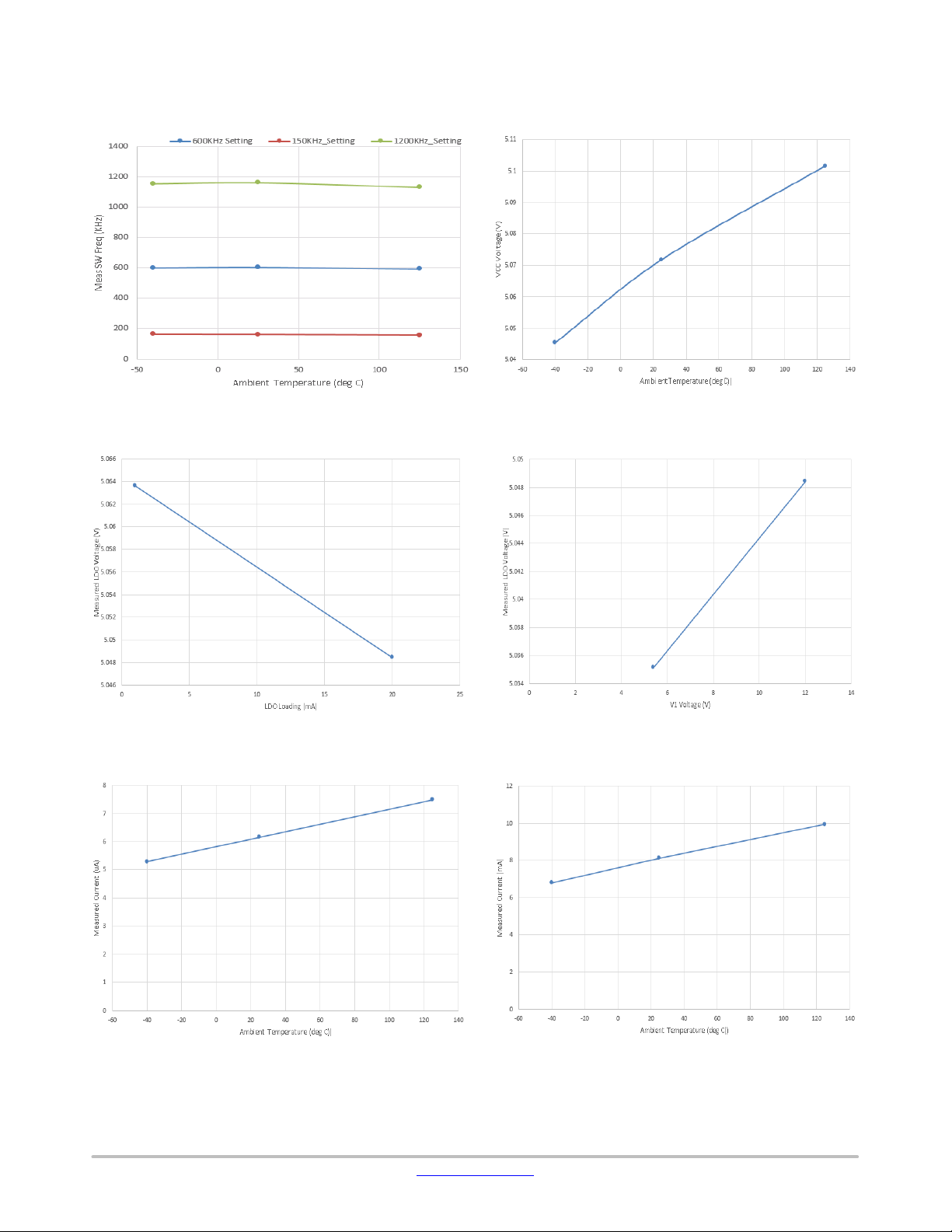
TYPICAL CHARACTERISTICS
Figure 1. Switching Frequency vs.
Temperature
Figure 3. VCC Load Regulation Figure 4. VCC Line Regulation (20 mA Load)
Figure 2. VCC vs. Temperature
Figure 5. Shutdown Supply Current vs.
Temperature
Figure 6. V1 Normal Current vs. Temperature
www.onsemi.com
10
Page 11

NCV81599, NCP81599
TYPICAL CHARACTERISTICS
6
5.5
5
4.5
4
3.5
VCCD Current (mA)
3
2.5
2
−50 0 50 100 150
Ambient Temperature (
C)°
Figure 7. VCCD Current vs. Temperature,
VCCD = 5.0 V
Figure 9. VDRIVE Switching Current Buck vs.
Temperature
Figure 8. ENABLE Rising Threshold vs.
Temperature
Figure 10. VDRIVE Switching Current Boost
vs. Temperature
Figure 11. Voltage Accuracy vs. Temperature
(FB Setting > 500 mV)
www.onsemi.com
Figure 12. Voltage Accuracy vs. Temperature
11
Page 12

NCV81599, NCP81599
TYPICAL CHARACTERISTICS
Figure 13. Voltage Ramp Up
(slew rate = 0.6 V/ms)
Figure 15. Voltage Ramp Up
(slew rate = 4.8 V/ms)
Figure 14. Voltage Ramp Down
(slew rate = 0.6 V/ms)
Figure 16. Voltage Ramp Down
(slew rate = 4.8 V/ms)
www.onsemi.com
12
Page 13

Vout
NCV81599, NCP81599
TYPICAL CHARACTERISTICS
Vout
Load current (2A/div)
Vin=24V, Vout=5V, Load=0.3A to 3A
Vin=24V, Vout=5V, Load=0.5A to 5A
Load current (2A/div)
Figure 17. 5 V Load Step Figure 18. 20 V Load Step
Figure 19. OCP Cycle−by−Cycle Waveform Figure 20. OCP Hiccup Waveform
Figure 21. OVP Waveform Figure 22. V2 Secondary OVP Waveform
www.onsemi.com
13
Page 14

NCV81599, NCP81599
TYPICAL CHARACTERISTICS
EN
Vsw2
Vsw1
Vout
Vin=12V, Vout=20V Vin=12V, Vout=20V
Figure 23. Shutdown by EN
Vout gradually walks down, after EN pin goes
Vout is discharged by load current, after EN pin
down from high (5V) to middle (1V)
Vsw1
Figure 24. Shutdown by EN
does down from high (5V) to low (0V)
EN
Vsw2
Vout
Figure 25. Efficiency vs. Load (MOSFET part number is NTMFS4C10N)
www.onsemi.com
14
Page 15

NCV81599, NCP81599
APPLICATION INFORMATION
Dual Edge Current Mode Control
When dual edge current mode control is used, two voltage
ramps are generated that are 180 degrees out of phase. The
inductor current signal is added to the ramps to incorporate
current mode control. In Figure 26, the COMP signal from
the compensation output interacts with two triangle ramps
to generate gate signals to the switches from S1 to S4. Two
ramp signals cross twice at midpoint within a cycle. When
COMP is above the midpoint, the system will operate at
Ramp1+i_sense
comp
Ramp2+i_sense
S1
S2
S3
boost mode with S1 always on and S2 always off, but S3 and
S4 turning on alternatively in an active switching mode.
When COMP is below the midpoint, the system will
operation at buck mode, with S4 always on and S3 always
off, but S1 and S2 turning on alternatively in an active
switching mode. The controller can switch between buck
and boost mode smoothly based on the COMP signal from
peak current regulation.
S4
L1S1
V1 V2
S2
Figure 26. Transitions for Dual Edge 4 Switch Buck Boost
S4
S3
www.onsemi.com
15
Page 16

NCV81599, NCP81599
Feedback and Output Voltage Profile
The feedback of the converter output voltage is connected
to the FB pin of the device through a resistor divider.
Internally FB is connected to the inverting input of the
internal transconductance error amplifier. The
non−inverting input of the gm amplifier is connected to the
internal reference. The internal reference voltage is by
default 0.5 V. Therefore a 10:1 resistor divider from the
in default. The reference voltage can be adjusted with
10 mV (default) or 5 mV steps from 0.1 V to 2.55 V through
the voltage profile register (01H), which makes the
continuous output voltage profile possible through an
external resistor divider. For example, by default, if the
external resistor divider has a 10:1 ratio, the output voltage
profile will be able to vary from 1 V to 25.5 V with 100 mV
steps.
converter output to the FB will set the output voltage to 5 V
Table 4. VOLTAGE PROFILE REGISTER SETTINGS
dac_target Isb
dac_target (01h)
bit_8 bit_7 bit_6 bit_5 bit_4 bit_3 bit_2 bit_1 bit_0
0 0 0 0 0 0 0 0 00 1 5
… … … … … … … … … … …
0 0 1 0 0 0 0 1 21 0 330
0 0 1 0 0 0 0 1 21 1 335
… … … … … … … … … … …
0 0 1 1 0 0 1 0 32 0 500 (Default)
… … … … … … … … … … …
1 1 0 0 1 0 0 0 C8 0 2000
… … … … … … … … … … …
1 1 1 1 1 1 1 1 FF 0 2550
1 1 1 1 1 1 1 1 FF 1 2555
dac_target (01h)
Hex Value
(03h, bit 4)
Reference DAC
Voltage (mV)
Transconductance Voltage Error Amplifier
To maintain loop stability under a large change in
capacitance, the NCV81599 can change the gm of the
internal transconductance error amplifier from 87 mS to
Table 5. AVAILABLE TRANSCONDUCTANCE SETTING
Address AMP_2 AMP_1 AMP_0
0 0 0 87
0 0 1 100
0 1 0 117
07h, bit [2:0]
Programmable Slew Rate
0 1 1 333
1 0 0 400
1 0 1 500 (default)
1 1 0 667
1 1 1 1000
The slew rate of the NCV81599 is controlled via the I2C
registers with the default slew rate set to 0.6 mV/ms
(FB = 0.1 V2, assume the resistor divider ratio is 10:1)
which is the slowest allowable rate change. The slew rate is
used when the output voltage starts from 0 V to a user
selected profile level, changing from one profile to another,
or when the output voltage is dynamically changed. The
1000 mS allowing the DC gain of the system to be increased
more than a decade triggered by the adding and removal of
the bulk capacitance or in response to another user input.
The default transconductance is 500 mS.
Amplifier GM Value (mS)
output voltage is divided by a factor of the external resistor
divider and connected to FB pin. The 9 Bit DAC is used to
increase the reference voltage in 10 or 5 mV increments. The
slew rate is decreased by using a slower clock that results in
a longer time between voltage steps, and conversely
increases by using a faster clock. The step monotonicity
depends on the bandwidth of the converter where a low
www.onsemi.com
16
Page 17

NCV81599, NCP81599
bandwidth will result in a slower slew rate than the selected
value. The available slew rates are shown in Table 6. The
selected slew rate is maintained unless the current limit is
DAC_TARGET
DAC_TARGET_LSB
V2
FB = 0.1*V2
Figure 27. Slew Rate Limiting Block Diagram and Waveforms
Table 6. SLEW RATE SELECTION
Soft Start or
Voltage Transition
Address Slew Bits
Slew_0
02h, bit [1:0]
Slew_1
Slew_2
Slew_3
(FB = 0.1*V2)
0.6 mV/ms
1.2 mV/ms
2.4 mV/ms
4.8 mV/ms
The discharge slew rate is accomplished in much the same
way as the charging except the reference voltage is
decreased rather than increased. The slew rate is maintained
unless the negative current limit is reached. If the negative
current limit is reached, the output voltage is decreased at the
maximum rate allowed by the current limit (see the negative
current limit section).
Soft−Start and EN Pin
During a 0 V soft−start, standard converters can start in
synchronous mode and have a monotonic rising of output
voltage. If a prebias exists on the output and the converter
starts in synchronous mode, the prebias voltage could be
discharged. The NCV81599 controller ensures that if a
prebias is detected, the soft−start is completed in a
non−synchronous mode to prevent the output from
discharging. During soft−start, the output rising slew rate
will follow the slew rate register with default value set to
0.6 mV/ms (FB = 0.1*V2).
tripped; in which case the increased voltage will be governed
by the positive current limit until the output voltage falls or
the fault is cleared.
V
2.56
9 bit DAC
VREF
+
−
CC
RC
CI
The EN Pin has 2 levels of threshold: the internal LDO and
2
I
C function are powered up when EN pin reaches ~0.8 V;
while the buck−boost conversion starts when EN pin reaches
~2.0 V. The EN pin can NOT work with very slow dv/dt
signals. Please always keep the EN pin input signal faster
than 0.5 V/ms. The EN pin has a pull−up current of ~3 mA,
so that an open EN pin powers up the NCV81599. To keep
the EN pin signal faster enough, please keep total
capacitance on the EN pin below 4.7 nF.
When the EN pin goes from high (above ENHT) down to
middle (below ENLT, but still above ENLDOHT), the
NCV81599 walks down the Vout gradually to zero, in the
discharge slew rate selected by “voltage transition slew rate”
register value, as shown in waveforms in Figure 23. All the
2
I
C register value stays.
When the EN pin goes from high (above ENHT) down to
low (below ENLDOLT), the NCV81599 stops all switching
immediately, and Vout is discharged by load current, as
shown in waveforms in Figure 24. Internal LDO shuts down,
and all I
Frequency Programming
2
C register value resets.
The switching frequency of the NCV81599 can be
programmed from 150 kHz to 1.2 MHz via the I
2
C interface.
The default switching frequency is set to 600 kHz. The
switching frequency can be changed on the fly. However, it
is a good practice to disable the part and then program to a
different frequency to avoid transition glitches at large load
current.
www.onsemi.com
17
Page 18

NCV81599, NCP81599
VCC
Internal Path
CS1 or CS2
Table 7. FREQUENCY PROGRAMMING TABLE
Name Bit Definition Description
Freq1 03H [2:0] Frequency Setting 3 Bits that Control the Switching Frequency from 150 kHz to 1.2 MHz.
000: 600 kHz (default)
001: 150 kHz
010: 300 kHz
011: 450 kHz
100: 750 kHz
101: 900 kHz
110: 1.2 MHz
111: Reserved
Current Sense Amplifiers
Internal precision differential amplifiers measure the
potential between the terminal CSP1 and CSN1 or CSP2 and
CSN2. Current flows from the input V1 to the output in a
buck boost design. Current flowing from V1 through the
switches to the inductor passes through R
external sense resistor, R
, has a significant effect on
SENSE
SENSE
. The
the function of current sensing and limiting systems and
must be chosen with care. First, the power dissipation in the
resistor should be considered. The system load current will
cause both heat and voltage loss in R
. The power loss
SENSE
and voltage drop drive the designer to make the sense
resistor as small as possible while still providing the input
dynamic range required by the measurement. Note that input
dynamic range is the difference between the maximum input
signal and the minimum accurately measured signal, and is
limited primarily by input DC offset of the internal
ILOAD
Rsense
5 mW
CSP1/CSP2
CSN1/CSN2
+
+
−
−
amplifier. In addition, R
V
does not exceed the maximum input voltage
SENSE
must be small enough that
SENSE
100 mV, even under peak load conditions.
The potential difference between CSPx and CSNx is level
shifted from the high voltage domain to the low voltage
VCC domain where the signal is split into two paths.
The first path, or external path, allows the end user to
observe the analog or digital output of the high side current
sense. The external path gain is set by the end user allowing
the designer to control the observable voltage level. The
voltage at CS1 or CS2 can be converted to 7 bits by the ADC
and stored in the internal registers which are accessed
through the I
2
C interface.
The second path, or internal path, has internally set gain
of 10 and allows cycle by cycle precise limiting of positive
and negative peak input current limits.
VCM
CLIND
10x(CSP1-CSN1)
+
−
10X
+
−
CLIP
10x(CSP2-CSN2)
CLIN
+
−
+
−
−
+
CS2 MUX
2
CS1 MUX
2
CS1
Positive Current
+
Limit
−
Negative Current
+
Limit
−
RAMP 1
RAMP 2
ADC
CS2
CS1
C
CS2
C
CS1
R
Figure 28. Block Diagram and Typical Connection for Current Sense
www.onsemi.com
18
R
CS2
Page 19
NCV81599, NCP81599
Positive Current Limit Internal Path
The NCV81599 has a pulse by pulse current limiting
function activated when a positive current limit triggers.
CSP1/CSN1 will be the positive current limit sense channel.
When a positive current limit is triggered, the current
pulse is truncated. In both buck mode and in boost mode the
S1 switch is turned off to limit the energy during an over
current event. The current limit is reset every switching
cycle and waits for the next positive current limit trigger. In
this way, current is limited on a pulse by pulse basis. Pulse
by pulse current limiting is advantageous for limiting energy
Table 8. INTERNAL PEAK CURRENT LIMIT
CLIN_1 CLIN_0 Address CSP2−CSN2 (mV)
0 0
0 1 −25 −5
1 0 −15 −3
1 1 0 0
CLIP_1 CLIP_0 Address CSP1−CSN1 (mV)
0 0
0 1 23 4.6
1 0 11 2.2
1 1 70 14
05h, bit[5:4]
05h, bit[1:0]
into a load in over current situations but are not up to the task
of limiting energy into a low impedance short. To address the
low impedance short, the NCV81599 does pulse by pulse
current limiting for 500 ms known as Ilim timeout, the
controller will enter into hiccup mode. The NCV81599
remains in fast stop state with all switches driven off for 10
ms. Once the 10 ms has expired, the part is allowed to soft
start to the previously programmed voltage and current level
if the short circuit condition is cleared.
The internal current limits can be controlled via the I
interface as shown in Table 8.
−40 (Default) −8
38 (Default) 7.6
Current at RSENSE = 5 mW (A)
Current at RSENSE = 5 mW (A)
2
C
Positive Current Limit Internal Latch−off
In addition to the positive current limit, there is a latch−off
over current protection, to provide quick protection against
output short and inductor saturation. The latch−off over
current protection, OCP_L, sensed across CSP2−CSN2
Table 9. THE LATCH−OFF CURRENT LIMIT OCP_L
CLIP_1 CLIP_0 Address
0 0
0 1 38 7.6
1 0 23 4.6
1 1 106 21.2
05h, bit[1:0]
Once the latch−off current limit protection is triggered, an
input OCP_L fault is set. All four switches are driven off
immediately. The OCP_L interrupt register bit set to 1. Only
toggling the EN or input power recycle can reset the part.
The latch−off current limit OCP_L can be disabled via I
2
C
register as shown in the following table.
Table 10. OCP_L LATCH−OFF CURRENT LIMIT
ENABLING AND DISABLING
Address Dis_OCP_L Description
04h, bit[1] 0 OCP_L Action Enabled
04h, bit[1] 1 OCP_L Action Disabled
Negative Current Limit Internal Path
Negative current limit can be activated in a few instances,
including light load synchronous operation, heavy load to
pins, has its threshold around twice that of the positive
current limit. As listed in the following table, OCP_L
threshold is set by the same I
CLIP_0, which set the internal positive peak current limit at
the same time.
CSP2−CSN2 (mV)
70 (Default) 14
Current at RSENSE = 5 mW (A)
light load transition, output overvoltage, and high output
voltage to lower output voltage transitions. CSP2/CSN2 will
be the negative current limit sense channel.
During light load synchronous operation, or heavy load to
light load transitions the negative current limit can be
triggered during normal operation. When the sensed current
exceeds the negative current limit, the S4 switch is shut off
preventing the discharge of the output voltage both in buck
mode and in boost mode if the output is in the power good
range. Both in boost mode and in buck mode when a
negative current is sensed, the S4 switch is turned off for the
remainder of either the S4 or S2 switching cycle and is
turned on again at the appropriate time. In buck mode, S4 is
turned off at the negative current limit transition and turned
on again as soon as the S2 on switch cycle ends. In boost
mode, the S4 switch is the rectifying switch and upon
2
C register bits, CLIP_1 and
www.onsemi.com
19
Page 20

NCV81599, NCP81599
negative current limit the switch will shut off for the
remainder of its switching cycle. The internal negative
current limits can be controlled via the I
2
C interface as
shown in Table 8.
External Path (CS1, CS2, CLIND)
The voltage drop across the sense resistors as a result of
the load can be observed on the CS1 and CS2 pins. Both
CS1, CS2 can be monitored with a high impedance input.
The voltage drop is converted into a current by a
transconductance amplifier with a typical GM of 5 mS. The
final gain of the output is determined by the end users
selection of the R
resistors. The output voltage of the CS
CS
pin can be calculated from Equation 1. The user must be
careful to keep the dynamic range below 2.56 V when
considering the maximum short circuit current.
VCS+ (I
RCS+
Table 11. REGISTER SETTING FOR THE CLIM COMPARATORS
AVERAGE*RSENSE
I
AVERAGE*RSENSE
Address CLIMx_1 CLIMx_0 CSx_LIM (V)
06h, bit [3:0]
* Trans) * RCSt 2.56 V å
V
CS
* Trans
0 0 0.25 .5 1
0 1 0.75 1.5 3
1 0 1.5 3 6
1 1
t
I
MAX
*R
2.56 V
SENSE
* Trans
(eq. 1)
2.5
The speed and accuracy of the dual amplifier stage allows
the reconstruction of the input and output current signal,
creating the ability to limit the peak current. If the user would
like to limit the mean DC current of the switch, a capacitor
can be placed in parallel with the R
resistors. CS1, CS2
CS
can be monitored with a high impedance input.
CS1, CS2 voltages are connected internally to 2 high
speed low offset comparators. When the external CLIND
flag is triggered, i.e, CLIND pin voltage is pulled high, it
indicates that one of the internal comparators has exceeded
the preset limit (CSx_LIM). The default comparator setting
is 250 mV which is a limit of 500 mA with a current sense
resistor of 5 mW and an R
resistor of 20 kW. The external
CS
current limit settings are shown in Table 11.
Current at RSENSE = 5 mW
RSET = 20 kW (A)
5 10
Current at RSENSE = 5 mW
RSET = 10 kW (A)
Overvoltage Protection (OVP)
When the divided output voltage is 15% (typical) above
the internal reference voltage for greater than one switching
cycle, an OV fault is set. During an overvoltage fault, S1 is
driven off, S2 is driven on, and S3 and S4 are modulated to
discharge the output while preventing the inductor current
from going beyond the I
2
C programmed negative current
limit.
L1S1
V1 V2
S2
Figure 29. Diagram for OV Protection
S4
S3
During overvoltage fault detection the switching
frequency changes from its I
2
C set value to 50 kHz to reduce
the power dissipation in the switches and prevent the
inductor from saturating. OVP is disabled during voltage
changes to ensure voltage changes and glitches during
slewing are not falsely reported as faults. The OVP faults are
reengaged 2 ms after completion of the soft start.
OV_REF
VFB
OV_MSK
Figure 30. OV Block Diagram
Input Overvoltage Lockout (OVLO) Protection
−
+
OV
The goal of the input OVLO fault detection is to protect
our IC from overvoltage damage and obtain regulation again
once the OVLO fault is cleared. OVLO can be a latched
shutdown or hiccup mode by a user register.
In a latched shutdown mode, when the input voltage is
higher than V
OVLOIN_R
for greater than the debounce time,
an input OVLO fault is set. All switches are driven off
immediately. The PG and input OVLO interrupt registers
are set to 1. Only toggling the EN or input power recycle can
reset the part.
In a hiccup mode, when the input voltage is higher than
V
OVLOIN_R
for greater than the debounce time, an input
OVLO fault is set. The OVLO debounce time is to filter any
overvoltage spike that is shorter than the time. During an
input OV fault, all switches are driven off immediately. The
www.onsemi.com
20
Page 21

NCV81599, NCP81599
DAC voltage is reset to 0. The PG and input OVLO interrupt
registers are set to 1. Once the input voltage falls under the
threshold, the debounce time starts counting. If input OVLO
keeps not detected during the OVLO recover debounce time,
a soft start will be reengaged.
Input OVLO detection starts from the beginning of
soft−start and ends in shutdown.
Output OVLO Protection and V2 Pin
The goal of the output OVLO fault detection is to protect
the MOSFET from overvoltage damage. The overvoltage
can be created by accidently write a wrong number in the
DAC_target register or installation problem on the external
feedback voltage divider. The default output OVLO
threshold is 30V. Customer can write to the 2−bit output
OVLO register 06h bit[5:4], sel_ov2th to configure the
threshold.
The output OVLO threshold can be set as 15V, 22.5V, 30V
and 36V, therefore it can be used for customer user cases that
requires a max output voltage of 10V, 15V, 20V and 25.5V,
respectively. Since most of the time, OVP should be able to
protect the output over voltage, the output OVLO threshold
are set >40% higher than the max output in that range. When
the output has run away due to either external voltage divider
or DAC configure error, output OVLO will kick into action.
Output OVLO has a latched shutdown mode. When the
output voltage is higher than the output OVLO threshold for
greater than the debounce time, an OVLO fault is set. The
output OVLO interrupt register will be set to 1. All switches
are driven off immediately. The PG and output OVLO
interrupt registers are set to 1. Toggling the EN or input
power recycle can reset the part.
Output OVLO detection starts from the beginning of
soft−start and ends in shutdown.
The output OVLO is sensed on the V2 pin. In some
extreme conditions, the V2 pin voltage, i.e. the output
voltage, may be pulled to negative, such as when the output
is short by a long cable. When V2 pin voltage goes negative,
the NCV81599 may enter a VCC UVLO, which resets all
registers to default and initial a soft−start. To prevent
negative voltage on V2 pin, a resistor, such as 1 kW, can be
placed between V2 pin and output voltage.
VTOP= 2.56 V
Gate
Signals
9R
R
VREF/SS
+
−
To
Driver
COMP
FB
V2
Code Gen
Profile Margin
Output
OVLO
Threshold
2
0.1*Vsw 2
M
U
X
9 bit DAC
1.5V, 2.2 5V,
3.0V, 3. 6V
−
+
Figure 31. Output OVLO
Power Good Monitor (PG)
NCV81599 provides two window comparators to monitor
the internal feedback voltage. The target voltage window is
±5% of the reference voltage (typical). Once the feedback
voltage is within the power good window, a power good
indication is asserted once a 3.3 ms timer has expired. If the
feedback voltage falls outside a ±7.5% window for greater
than 1 switching cycle, the power good register is reset.
Power good is indicated on the INT pin if the I
2
C register is
set to display the PG state. When DAC is set to below
400 mV, the PG high threshold is kept at a constant voltage,
and the PG low threshold is kept at 0 to avoid false
triggering.
PG_MSK
PG_Low
VFB
PG_High
−
+
−
+
PG
V2
www.onsemi.com
21
Figure 32. PG Block Diagram
Page 22

107.5%
105%
100%Vref
95%
92.5%
Power Not Good
V
FB
Power Not Good
NCV81599, NCP81599
Power Good
S4
L
S3
NCV81599
PDRV
VBUS
10μF
USB port
PG
Figure 33. Power Good Diagram
Thermal Shutdown
The NCV81599 protects itself from overheating with an
internal thermal shutdown circuit. If the junction
temperature exceeds the thermal shutdown threshold
(typically 150°C), all MOSFETs will be driven to the off
state, and the part will wait until the temperature decreases
to an acceptable level. The fault will be reported to the fault
register and the INT flag will be set unless it is masked.
When the junction temperature drops below 125°C
(typical), the part will discharge the output voltage to Vsafe
0V.
PFET Drive
The PMOS drive is an open drain output used to control
the turn on and turn off of PMOSFET switches at a floating
potential. The external PMOS can be used as a cutoff switch,
enable for an auxiliary power supply, or a bypass switch for
a power supply. The RDSon of the pulldown NMOSFET is
typically 20 W allowing the user to quickly turn on large
PMOSFET power channels.
Table 12. PFET ACTIVATION TABLE
Address PFET_DRV Description
04h, bit [0]
0 NFET OFF (Default)
1 NFET ON
PFET_DRV
Figure 34. PFET Drive
Analog to Digital Converter
The analog to digital converter is a 7−bit A/D which can
be used as an event recorder, an input voltage sampler,
output voltage sampler, input current sampler, or output
current sampler. The converter digitizes real time data
during the sample period. The internal precision reference is
used to provide the full range voltage; in the case of V1(input
voltage), or FB (with 10:1 external resistor divider) the full
range is 0 V to 25.5 V. The V1 is internally divided down by
10 before it is digitized by the ADC, thus the range of the
measurement is 0 V−2.55 V, same as FB. The resolution of
the V1 and FB voltage is 20 mV at the analog mux, but since
the voltage is divided by 10 output voltage resolution will be
200 mV. Therefore, the highest input voltage report is
200 mV x 127 = 25.4 V. When CS1 and CS2 are sampled, the
range is 0 V−2.55 V. The resolution will be 20 mV in the CS
monitoring case. The actual current can be calculated by
dividing the CS1 or CS2 values with the factor of Rsense ×
5mS × RCSx, the total gain from the current input to the
external current monitoring outputs.
www.onsemi.com
22
Page 23

0.1*V1
NCV81599, NCP81599
Figure 35. Analog to Digital Converter
Table 13. ADC RESULT BYTE
Address MSB 5 4 3 2 1 LSB
10h, 11h, 12h, 13h D6 D5 D4 D3 D2 D1 D0
Table 14. REGISTER SETTING FOR ENABLING DESIRED ADC BEHAVIOUR
Address ADC_2 ADC_1 ADC_0 Description
08h, bit [4:2]
0 0 0
0 0 1
0 1 0
0 1 1
1 0 0
Set Amux to VFB
Sets Amux to V1
Set Amux to CS2
Set Amux to CS1
Select all in rotating sequence (VFB, V1, CS2, CS1, VFB, …)
Table 15. REGISTER SETTING FOR ADC TRIGGER MANNER
Address ADC Trigger Description
08h, bit [1:0]
00
01
10
Trigger a 1x read by a fault condition (Default)
Trigger a 1x read
Trigger a continuous read
Interrupt Control
The interrupt controller continuously monitors internal
interrupt sources, generating an interrupt signal when a
system status change is detected. Individual bits generating
2
interrupts will be set to 1 in the INTACK register (I
C read
only registers), indicating the interrupt source. INTACK
register is automatically reset by an I
2
C read. All interrupt
sources can be masked by writing 1 in register INTMSK of
09h and 0Ah. Masked sources will never generate an
interrupt request on the INT pin. The INT pin is an open
drain output. A non−masked interrupt request will result in
the INT pin being driven high. When the host reads the
INTACK registers, the INT pin will be driven low and the
interrupt register INTACK is cleared. Figure 36 illustrates
the interrupt process.
www.onsemi.com
23
Page 24

OCP_L
OCP_L_MASK
V2OVP
V2OVP_MASK
V1OVP
V1OVP_MASK
TSD
TSD_MASK
OCP_P
OCP_P_MASK
OV
OV_MASK
CLIND
CLIND_MASK
PG_BAR
NCV81599, NCP81599
INT
PG_BAR_MASK
VCHN
VCHN_MASK
Figure 36. Interrupt Logic
Table 16. INTERPRETATION TABLE
Interrupt Name Register name Address Description
OCP_L ocp_l 14h, bit [6] Internal positive over current latch−off
V2OVP v2ovp 14h, bit [5] Output secondary over voltage
V1OVP v1ovp 14h, bit [4] Input over voltage
TSD tsd 14h, bit [3] Thermal shut down
OCP_P ocp_p 14h, bit [2] Internal positive over current
OV ov 14h, bit [1] Output over voltage
CLIND ext_clind_ocp 14h, bit [0] External over current trip from CLIND
VCHN vchn 15h, bit [1] Output negative voltage change
PG_BAR pg_int 15h, bit [0] Power good bar thresholds exceeded
I2C Address and Registers
NCV81599 can set up to 4 different I2C addresses by
sensing the shunt resistor voltage at ADDR pin. The chip
will source a 10 mA current to the ADDR resistor and sense
the voltage corresponding to different I2C addresses
everytime when it is powered on. Suggest to put resistors of
0 W, 26.1 kW, 44.2 kW, 71.5 kW from ADDR pin to GND to
set I2C address 74H, 75H, 76H, 77H respectively.
Unused bits in the register map below are marked with
“−”. Writing either “1” or “0” into these unused bits in
user−programmable registers does NOT change any
function/performance of the NCV81599.
www.onsemi.com
24
Page 25

Table 17. I2C REGISTER MAP BIT DETAIL
ADDR
(Hex)
00h − − 0 0 en_int en_mask − − 00h
01h dac_target 32h
02h − − − − − − slew_rate 00h
03h − − v1ovp_lat dac_target_isb − pwm_frequency 00h
04h − − cs2_dchrg cs1_dchrg − − dis_ocp_l pfet 00h
05h − − ocp_clim_neg − − ocp_clim_pos 00h
06h − − sel_ov2th cs2_clim_pos cs1_clim_pos 20h
07h − − − − − gm_amp_setting 05h
08h − − dis_adc amux_sel amux_trigger 00h
User−programmable Registers
09h − int_mask
0Ah − − − − − − int_mask_vchn int_mask_pg 00h
− 0B .. 0Fh
10h − vfb
11h − vin
12h − cs2
13h − cs1
Registers
14h − ocp_l v2ovp v1ovp tsd ocp_p ov ext_clind_ocp
User Read−only
15h − − − − − − vchn pg_int
Bit 7 Bit 6 Bit 5 Bit 4 Bit 3 Bit 2 Bit 1 Bit 0 Default
_ocp_l
int_mask_v2ovp int_mask_v1ovp int_mask_tsd int_mask_ocp_p int_mask_ov int_mask_clind 00h
NCV81599, NCP81599
www.onsemi.com
25
Page 26

NCV81599, NCP81599
I2C Interface
The I2C interface can support 5 V TTL, LVTTL, 2.5 V and
1.8 V interfaces with two precision SCL and SDA
comparators with 1 V thresholds shown in Figure 37. The
part cannot support 5 V CMOS levels as there can be some
ambiguity in voltage levels.
I2C Compatible Interface
The NCV81599 can support a subset of I2C protocol as
detailed below. The NCV81599 communicates with the
5V CMOS
Vcc =4.5V−5.5V
V
OH
V
IH
V
TH
V
IL
VOL=0.5V
=4.44V
= 0.7*vcc
= 0.5*vcc
= 0.3*vcc
TTL
Vcc =4.5V−5.5V
V
OH
V
IH
VTH = 1.5V
V
IL
VOL=0.4V
Vcc =2.7V−3.6V
EIS/JEDEC 8−5
=2.4V
=2.0V
=0.8V
LVTTL
V
V
V
OH
V
IH
IL
OL
=2.4V
=2.0V
=0.8V
=0.4V
external processor by means of a serial link using a 400 kHz
up to 1.2 MHz I
2
C two−wire interface protocol. The I2C
interface provided is fully compatible with the Standard,
2
Fast, and High−Speed I
C modes. The NCV81599 is not
intended to operate as a master controller; it is under the
control of the main controller (master device), which
controls the clock (pin SCL) and the read or write operations
through SDA. The I
2
C bus is an addressable interface (7−bit
addressing only) featuring two Read/Write addresses.
2. 5
Vcc =2.3V−2.7V
EIS/JEDEC 8−5
V
OH
V
IH
V
IL
V
OL
=2.0V
=1.7V
=0.7V
=0.4V
1.8V
Vcc =1.65V−1.95V
EIS/JEDEC 8−7
= VCC−0.45V
V
OH
= 0.65*Vcc
V
IH
= 0.35*Vcc
V
IL
=0.45V
V
OL
1.0V Threshold
Figure 37. I2C Thresholds and Comparator Thresholds
I2C Communication Description
The first byte transmitted is the chip address (with the LSB
bit set to 1 for a Read operation, or set to 0 for a Write
operation). Following the 1 or 0, the data will be:
• In case of a Write operation, the register address
(@REG) pointing to the register for which it will be
written is followed by the data that will written in that
location. The writing process is auto−incremental, so
From MCU to NCV81599
From NCV81599 to MCU
Start IC ADDRESS 1 ACK DATA 1 ACK Data n /ACK STOP
1 Read
Start IC ADDRESS 0 ACK DATA 1 ACK Data n STOP Write Inside Part
the first data will be written in @REG, the contents of
@REG are incremented, and the next data byte is
placed in the location pointed to @REG + 1..., etc.
• In case of a Read operation, the NCV81599 will output
the data from the last register that has been accessed by
the last write operation. Like the writing process, the
reading process is auto−incremental.
/ACK
ACK
READ OUT
FROM PART
0 Write
If part does not Acknowledge, the /NACK will be followed by a STOP or Sr. If part
Acknowledges, the ACK can be followed by another data or STOP or Sr.
Figure 38. General Protocol Description
www.onsemi.com
26
Page 27

NCV81599, NCP81599
Read Out from Part
The master will first make a “Pseudo Write” transaction
with no data to set the internal address register. Then, a stop
From MCU to NCV81599
From NCV81599 to MCU
Start IC ADDRESS 0 ACK
0 Write
Start IC ADDRESS 1 ACK DATA 1 ACK Data n STOP Write Inside Part
1 Read
From MCU to NCV81599
Sets Internal
Register Pointer
Register Address ACK STOP
Register Address
Value
Figure 39. Read Out From Part
then start or a repeated start will initiate the Read transaction
from the register address the initial Write transaction was
pointed to:
/ACK
Register Address + (n+1)
Value
N Register Read
From NCV81599 to MCU
Start IC ADDRESS 0 ACK Register REG Address ACK
0 Write
Start IC ADDRESS 1 ACK DATA 1 ACK Data n STOP
1 Read
Sets Internal
Register Pointer
Register Address + (n−1)
Value
k Register Read
Figure 40. Write Followed by Read Transaction
Write In Part
Write operation will be achieved by only one transaction.
After the chip address, the MCU first data will be the internal
From MCU to NCV81599
From NCV81599 to MCU
Start IC ADDRESS 0 ACK Register REG Address ACK
Sets Internal
Register pointer
Write Value in
Register REG
REG Value
Register Address + (n+1) +
(k−1) Value
ACK
N Register Read
/ACK
Write Value in
Register REG + (n−1)
REG + (n−1) Value
ACK
register desired to access, the following data will be the data
written in REG, REG + 1, REG + 2, ..., REG + (n−1).
Write Value in
Register REG
REG Value
ACK
Write Value in
Register REG + (n−1)
REG + (n−1) Value
STOP
ACK
STOP
0 Write
N Register Read
Figure 41. Write in n Registers
www.onsemi.com
27
Page 28

NCV81599, NCP81599
I2C Communication Considerations
• It takes at least 3.3 ms for the digital core to reset all the
registers, so it is recommended not to change the
register value until at least 3.3 ms after the output
voltage finish ramping to a steady state.
• It is recommended to avoid setting reference voltage
profile below 0.1 V. When 0 V output is needed, it is
recommended to ramp down the output by pulling EN
pin low with external circuit or by I2C communication
in the firmware. Setting output voltage profile to 0 via
I2C is not recommended.
www.onsemi.com
28
Page 29

NCV81599, NCP81599
DESIGN CONSIDERATIONS
dv/dt Induced False Turn On
In synchronous buck converters, there is a well−known
phenomenon called “low side false turn−on,” or “dv/dt
induced turn on”, which can be potentially dangerous for the
switch itself and the reliability of the entire converter. The
Vgs’
+
−
Vsw1
C
gd
C
gs
Vin
S1
Drain
S2
Source
L
dV/dt
Buck phase dv/dt induced false
turn on equivalent circuit
4−Switch
Buck−boost
Controller
R
pu_ds(on)
R
LSG1
pd_ds(on)
GND
R
g_ext
Figure 42. dv/dt Induced False Turn−on Equivalent Circuit of a 4−switch Buck−boost Converter
Gate
R
g_int
Figure 42 shows false turn on equivalent circuit of the
buck phase and the boost phase at the moment a positive
dv/dt transition appears across the drain−to−source junction.
The detailed analysis of this phenomenon can be found in
Gate Driver Design Considerations for 4−Switch
Buck−Boost Converters.
Select the Switching Power MOSFET
The MOSFETs used in the power stage of the converter
should have a maximum drain−to−source voltage rating that
exceeds the sum of steady state maximum drain−to−source
voltage and the turn−off voltage spike with a considerable
margin (20%~50%).
When selecting the switching power MOSFET, the
MOSFET gate capacitance should be considered carefully
to avoid overloading the 5 V LDO. For one MOSFET, the
allowed maximum total gate charge Q
can be estimated by
g
Equation 2:
I
driver
where I
Qg+
f
sw
is the gate drive current and fsw is the switching
driver
(eq. 2)
frequency.
It is recommended to select the MOSFETs with smaller
than 3 nF input capacitance (C
). The gate threshold
iss
voltage should be higher than 1.0 V due to the internal
adaptive non−overlap gate driver circuit.
In order to prevent dv/dt induced turn−on, the criteria for
selecting a rectifying switch is based on the Q
Q
is the gate−to−source charge before the gate voltage
gs(th)
reaches the threshold voltage. Lowering C
gd/Qgs(th)
gd
ratio.
will reduce
dv/dt induced voltage magnitude. Moreover, it also depends
4−switch buck−boost converter is not exempt from this
issue. To make things worse, errors are made when designers
simply copy the circuit parameters of a buck converter
directly to the boost phase of the 4−switch buck−boost
converter.
Vgs’
Vout
Drain
C
gd
S4
+
C
gs
−
Source
Vsw2
S3
dV/dt
L
4−Switch
Buck−boost
Controller
R
pu_ds(on)
R
g_ext
HSG2
R
pd_ds(on)
Vsw2
Boost phase dv/dt induced
false turn on equivalent circuit
on dt/C
, Vds and threshold voltage Vth. One way of
gs
Gate
R
g_int
interpreting the dv/dt induced turn−on problem is when V
reaches the input voltage, the Miller charge should be
smaller than the total charge on C
at the Vth level, so that
gs
the rectifying switches will not be turned on. Then we will
have the following relation:
C
Vgs+
gd
Cgd) C
Qgdt Q
Vdst V
gs
GS(th)
gs(th)
(eq. 3)
(eq. 4)
We can simply use Equation 4 to evaluate the rectifying
device’s immunity to dv/dt induced turn on. Ideally, the
charge Q
should not be greater than 1.5*Q
gd
gs(th)
in order to
leave enough margin.
Select Gate Drive Resistors
To increase the converter’s dv/dt immunity, the dv/dt
control is one approach which is usually related to the gate
driver circuit. A first intuitive method is to use higher pull
up resistance and gate resistance for the active switch. This
would slow down the turn on of the active switch, effectively
decreasing the dv/dt. Table 18 shows the recommended
value for MOSFETs’ gate resistors.
Table 18. RECOMMENDED VALUE for Gate Resistors
Buck Phase Boost Phase
HSG1
LSG1
(3.3~5.1)W
0W
HSG2
LSG2
0W
(3.3~5.1)W
An alternative approach is to add an RC snubber circuit to
the switching nodes V
sw1
and V
. This is the most direct
sw2
ds
www.onsemi.com
29
Page 30

NCV81599, NCP81599
way to reduce the dv/dt. The side effect of the above two
methods are that losses would be increased because of slow
switching speed.
LAYOUT GUIDELINES
Electrical Layout Considerations
Good electrical layout is a key to make sure proper
operation, high efficiency, and noise reduction.
• Current Sensing: Run two dedicated trace with decent
width in parallel (close to each other to minimize the
loop area) from the two terminals of the input side or
output side current sensing resistor to the IC. Place the
common−mode RC filter components in general
proximity of the controller.
Route the traces into the pads from the inside of the current
sensing resistor. The drawing below shows how to rout the
traces.
Current Path
PCB Trace
Current Sense
Resistor
CSP/CSN
• Gate Driver: Run the high side gate, low side gate and
switching node traces in a parallel fashion with decent
width. Avoid any sensitive analog signal trace from
crossing over or getting close. Recommend routing
Vsw1/2 trace to high−side MOSFET source pin instead
of copper pour area. The controller should be placed
close to the switching MOSFETs gate terminals and
keep the gate drive signal traces short for a clean
MOSFET drive. It’s OK to place the controller on the
opposite side of the MOSFETs.
• I2C Communication: SDA and SCL pins are digital
pins. Run SDA and SCL traces in parallel and reduce
the loop area. Avoid any sensitive analog signal trace or
noise source from crossing over or getting close.
• V1 Pin: Input for the internal LDO. Place a decoupling
capacitor in general proximity of the controller. Run a
dedicated trace from system input bus to the pin and do
not route near the switching traces.
• VCC Decoupling: Place decoupling caps as close as
possible to the controller VCC pin. Place the RC filter
connecting with VDRV pin in general proximity of the
controller. The filter resistor should be not higher than
10 W to prevent large voltage drop.
• VDRV Decoupling: Place decoupling caps as close as
possible to the controller VDRV pin.
• Input Decoupling: The device should be well
decoupled by input capacitors and input loop area
should be as small as possible to reduce parasitic
inductance, input voltage spike, and noise emission.
Usually, a small low−ESL MLCC is placed very close
to the input port. Place these capacitors on the same
PCB layer with the MOSFETs instead of on different
layers and using vias to make the connection.
• Output Decoupling: The output capacitors should be
as close as possible to the load.
• Switching Node: The converter’s switching node
should be a copper pour to carry the current, but
compact because it is also a noise source of electrical
and magnetic field radiation. Place the inductor and the
switching MOSFETs on the same layer of the PCB.
• Bootstrap: The bootstrap cap and an option resistor
need to be in general close to the controller and directly
connected between pin BST1/2 and pin SW1/2
respectively.
• Ground: It would be good to have separated ground
planes for PGND and AGND and connect the AGND
planes to PGND through a dedicated net tie or 0 W
resistor.
• Voltage Sense: Route a “quiet” path for the input and
output voltage sense. AGND could be used as a remote
ground sense when differential sense is preferred.
• Compensation Network: The compensation network
should be close to the controller. Keep FB trace short to
minimize it capacitance to ground.
Thermal Layout Considerations
Good thermal layout helps power dissipation and junction
temperature reduction.
• The exposed pads must be well soldered on the board.
• A four or more layers PCB board with solid ground
planes is preferred for better heat dissipation.
• More free vias are welcome to be around IC and
underneath the exposed pads to connect the inner
ground layers to reduce thermal impedance.
• Use large area copper pour to help thermal conduction
and radiation.
• Do not put the inductor too close to the IC, thus the heat
sources are distributed.
www.onsemi.com
30
Page 31

QFNW32 5x5, 0.5P
8
MECHANICAL CASE OUTLINE
PACKAGE DIMENSIONS
32
1
SCALE 2:1
PIN ONE
REFERENCE
0.10 C
0.08 C
NOTE 4
DETAIL A
32X
L
K
D
TOP VIEW
DETAIL B
C
C
SIDE VIEW
D2
9
8
1
32
e
e/2
BOTTOM VIEW
RECOMMENDED
SOLDERING FOOTPRINT*
1
25
5.30
3.35
A
B
L
E
A
(A3)
SEATING
C
PLANE
17
E2
32X
b
M
0.10 BC
M
0.05 C
A1
32X
0.63
A4
A
NOTE 3
CASE 484AB
ISSUE D
L3
L4
L
ALTERNATE
EXPOSED
COPPER
PLATING
DETAIL B
PLATED
SURFACES
CONSTRUCTION
A4
SECTION C−C
DETAIL A
ALTERNATE
CONSTRUCTION
L3
DATE 07 SEP 201
L3
L4
NOTES:
1. DIMENSIONS AND TOLERANCING PER
ASME Y14.5M, 1994.
2. CONTROLLING DIMENSION: MILLIMETERS.
3. DIMENSION b APPLIES TO PLATED
TERMINAL AND IS MEASURED BETWEEN
0.10 AND 0.20MM FROM THE TERMINAL TIP.
4. COPLANARITY APPLIES TO THE EXPOSED
PAD AS WELL AS THE TERMINALS.
MILLIMETERS
DIM MIN NOM
A4
A1
A3
A 0.80 0.90
A1 −−− −−−
A3 0.20 REF
A4
0.10 −−− −−−
b 0.20 0.25
D
4.90 5.00
D2 3.00 3.10
E
4.90 5.00
E2 3.00 3.10
e 0.50 BSC
K
0.35 −−− −−−
L 0.30 0.40
L3
−−− −−− 0.10
L4 0.08 REF
MAX
1.00
0.05
0.30
5.10
3.20
5.10
3.20
0.50
GENERIC
MARKING DIAGRAM*
1
XXXXXXXX
XXXXXXXX
AWLYYWWG
G
XXXXX = Specific Device Code
A = Assembly Location
WL = Wafer Lot
YY = Year
WW = Work Week
G = Pb−Free Package
(Note: Microdot may be in either location)
*This information is generic. Please refer to
device data sheet for actual part marking.
Pb−Free indicator, “G” or microdot “G”, may
or may not be present. Some products may
not follow the Generic Marking.
3.35
PACKAGE
OUTLINE
0.50
PITCH
DIMENSION: MILLIMETERS
32X
0.30
5.30
*For additional information on our Pb−Free strategy and soldering
details, please download the ON Semiconductor Soldering and
Mounting Techniques Reference Manual, SOLDERRM/D.
DOCUMENT NUMBER:
DESCRIPTION:
ON Semiconductor and are trademarks of Semiconductor Components Industries, LLC dba ON Semiconductor or its subsidiaries in the United States and/or other countries.
ON Semiconductor reserves the right to make changes without further notice to any products herein. ON Semiconductor makes no warranty, representation or guarantee regarding
the suitability of its products for any particular purpose, nor does ON Semiconductor assume any liability arising out of the application or use of any product or circuit, and specifically
disclaims any and all liability, including without limitation special, consequential or incidental damages. ON Semiconductor does not convey any license under its patent rights nor the
rights of others.
© Semiconductor Components Industries, LLC, 2018
98AON14940G
QFNW32 5x5, 0.5P
Electronic versions are uncontrolled except when accessed directly from the Document Repository.
Printed versions are uncontrolled except when stamped “CONTROLLED COPY” in red.
PAGE 1 OF 1
www.onsemi.com
Page 32

MECHANICAL CASE OUTLINE
PACKAGE DIMENSIONS
32
1
SCALE 2:1
PIN ONE
REFERENCE
0.15 C
0.10 C
0.08 C
NOTE 4
DETAIL A
D
0.15
C
TOP VIEW
DETAIL B
(A3)
SIDE VIEW
D2
8
E2
1
32
e
e/2
BOTTOM VIEW
RECOMMENDED
SOLDERING FOOTPRINT*
5.30
3.70
A
B
E
A
A1
C
K
17
32X
32X
L
b
M
0.10 BC
M
0.05 C
32X
0.62
24
25
QFN32 5x5, 0.5P
CASE 485CE
ISSUE O
L1
CONSTRUCTIONS
SEATING
PLANE
A-B
NOTE 3
L
DETAIL A
ALTERNATE
DETAIL B
ALTERNATE
CONSTRUCTION
L
MOLD CMPDEXPOSED Cu
NOTES:
1. DIMENSIONING AND TOLERANCING PER
ASME Y14.5M, 1994.
2. CONTROLLING DIMENSION: MILLIMETERS.
3. DIMENSION b APPLIES TO PLATED
TERMINAL AND IS MEASURED BETWEEN
0.15 AND 0.30 MM FROM THE TERMINAL TIP.
4. COPLANARITY APPLIES TO THE EXPOSED
PAD AS WELL AS THE TERMINALS.
MILLIMETERS
DIM MIN MAX
A 0.80 1.00
A1 −−− 0.05
A3 0.20 REF
b 0.20 0.30
D 5.00 BSC
D2 3.40 3.60
E 5.00 BSC
E2
3.40 3.60
e 0.50 BSC
K 0.20 −−−
L 0.30 0.50
L1 −−− 0.15
GENERIC
MARKING DIAGRAM*
1
XXXXXXXX
XXXXXXXX
AWLYYWWG
XXXXX = Specific Device Code
A = Assembly Location
WL = Wafer Lot
YY = Year
WW = Work Week
G = Pb−Free Package
*This information is generic. Please refer
to device data sheet for actual part
marking.
Pb−Free indicator, “G” or microdot “ G”,
may or may not be present.
DATE 07 FEB 2012
3.70
0.50
PITCH
DIMENSIONS: MILLIMETERS
5.30
32X
0.30
*For additional information on our Pb−Free strategy and soldering
details, please download the ON Semiconductor Soldering and
Mounting Techniques Reference Manual, SOLDERRM/D.
DOCUMENT NUMBER:
DESCRIPTION:
ON Semiconductor and are trademarks of Semiconductor Components Industries, LLC dba ON Semiconductor or its subsidiaries in the United States and/or other countries.
ON Semiconductor reserves the right to make changes without further notice to any products herein. ON Semiconductor makes no warranty, representation or guarantee regarding
the suitability of its products for any particular purpose, nor does ON Semiconductor assume any liability arising out of the application or use of any product or circuit, and specifically
disclaims any and all liability, including without limitation special, consequential or incidental damages. ON Semiconductor does not convey any license under its patent rights nor the
rights of others.
© Semiconductor Components Industries, LLC, 2019
98AON34336E
TDFN8, 2X3, 0.5P
Electronic versions are uncontrolled except when accessed directly from the Document Repository.
Printed versions are uncontrolled except when stamped “CONTROLLED COPY” in red.
PAGE 1 OF 1
www.onsemi.com
Page 33

ON Semiconductor and are trademarks of Semiconductor Components Industries, LLC dba ON Semiconductor or its subsidiaries in the United States and/or other countries.
ON Semiconductor owns the rights to a number of patents, trademarks, copyrights, trade secrets, and other intellectual property. A listing of ON Semiconductor ’s product/patent
coverage may be accessed at www.onsemi.com/site/pdf/Patent−Marking.pdf
ON Semiconductor makes no warranty, representation or guarantee regarding the suitability of its products for any particular purpose, nor does ON Semiconductor assume any liability
arising out of the application or use of any product or circuit, and specifically disclaims any and all liability, including without limitation special, consequential or incidental damages.
Buyer is responsible for its products and applications using ON Semiconductor products, including compliance with all laws, regulations and safety requirements or standards,
regardless of any support or applications information provided by ON Semiconductor. “Typical” parameters which may be provided in ON Semiconductor data sheets and/or
specifications can and do vary in different applications and actual performance may vary over time. All operating parameters, including “Typicals” must be validated for each customer
application by customer’s technical experts. ON Semiconductor does not convey any license under its patent rights nor the rights of others. ON Semiconductor products are not
designed, intended, or authorized for use as a critical component in life support systems or any FDA Class 3 medical devices or medical devices with a same or similar classification
in a foreign jurisdiction or any devices intended for implantation in the human body. Should Buyer purchase or use ON Semiconductor products for any such unintended or unauthorized
application, Buyer shall indemnify and hold ON Semiconductor and its officers, employees, subsidiaries, affiliates, and distributors harmless against all claims, costs, damages, and
expenses, and reasonable attorney fees arising out of, directly or indirectly, any claim of personal injury or death associated with such unintended or unauthorized use, even if such
claim alleges that ON Semiconductor was negligent regarding the design or manufacture of the part. ON Semiconductor is an Equal Opportunity/Affirmative Action Employer. This
literature is subject to all applicable copyright laws and is not for resale in any manner.
. ON Semiconductor reserves the right to make changes without further notice to any products herein.
PUBLICATION ORDERING INFORMATION
LITERATURE FULFILLMENT:
Email Requests to: orderlit@onsemi.com
ON Semiconductor Website: www.onsemi.com
TECHNICAL SUPPORT
North American Technical Support:
Voice Mail: 1 800−282−9855 Toll Free USA/Canada
Phone: 011 421 33 790 2910
Europe, Middle East and Africa Technical Support:
Phone: 00421 33 790 2910
For additional information, please contact your local Sales Representative
◊
www.onsemi.com
1
 Loading...